Apple Announces New Updated iPhone SE: A13 & New Features for $399

Apple’s last “classic” iPhone release was the iPhone 8 back in 2017, with the 2016 iPhone SE (Special Edition) being the last iteration donning the iPhone 4 design language. It’s safe to say both these devices had been getting a bit long in the tooth, and there’s still plenty of people out there which loved the 4.7” form-factor – and possibly unwilling to update to the newer bigger models.


Luckily, Apple seemingly agrees that this market is worth covering, and today announced a refresh of the 2016 iPhone SE. The new 2020 special edition model takes its design queues from the iPhone 8, essentially taking it as a blueprint for the shell of the phone, and crams in the latest hardware technology that were premiered with the iPhone 11 series.


Most importantly, Apple is offering this new small fierce package at an incredible price point starting at $399, significantly cheaper than even the “lower-end” iPhone 11. The combination seems an outright winner, let’s go over the specifications:


Apple 2019-2020 iPhone Specifications
  iPhone 11 Pro iPhone 11 Pro Max iPhone 11

iPhone SE

(2020)

SoC Apple A13 Bionic


2 × Lightning Performance @ 2.66GHz

8MB L2


4 × Thunder Efficiency @ 1.73GHz

4MB L2

GPU Apple, 4 Cores
DRAM 4GB LPDDR4X ??
Display 5.8-inch OLED

2436×1125

DCI-P3/True Tone

800 cd/m² brightness

2M:1 contrast ratio
3D Touch
6.5-inch OLED

2688×1242

DCI-P3/True Tone

800 cd/m² brightness

2M:1 contrast ratio
3D Touch
6.1-inch LCD

1792×828

DCI-P3/True Tone

625 cd/m² brightness

1400:1 contrast ratio

4.7-inch LCD

1334×750

DCI-P3/True Tone

625 cd/m² brightness

1400:1 contrast ratio

Size Height 144.0 mm 158.0 mm 150.9 mm 138.4 mm
Width 71.4 m 77.8 mm 75.7 mm 67.3 mm
Depth 8.1 mm 8.1 mm 8.3 mm 7.3 mm
Weight 188 grams 226 grams 194 grams 148 grams
Battery Life 3046mAh


+14.5% capacity
“+4H vs XS”

3969mAh


+25% capacity
“+5H vs XS Max”

3110mAh


+5.7% capacity
“+1H vs XR”

??
Wireless Charging Qi
Rear Cameras Main 12 MP 1.4µm Dual Pixel PD


f/1.8, OIS


Wide Color Gamut

Quad LED True Tone Flash

12 MP 1.4µm


f/1.8, OIS


Wide Color Gamut

Quad LED True Tone Flash

Tele-

Photo
12 MP f/2.0 Telephoto, OIS

2x Optical Zoom
Wide 12MP f/2.4

120° Ultra-wide Angle
Front Camera 12MP f/2.2 Wide Angle 7MP f/2.2
Storage 64 GB

256 GB

512 GB
64 GB

256 GB

512 GB
64 GB

128 GB

256 GB
64 GB

128 GB

256 GB
I/O Apple Lightning
Wireless (local) 802.11ax Wi-Fi with MIMO + Bluetooth 5.0 + NFC
Cellular Gigabit-class LTE-A

4×4 MIMO and LAA
Gigabit-class

LTE-A

2×2 MIMO and LAA
Gigabit-class

LTE-A
Splash, Water, Dust Resistance IP68

up to 2 meters (Pro models = 4 meters), up to 30 minutes
IP67

up to 1 meters, up to 30 minutes
Dual-SIM nano-SIM + eSIM

nano-SIM + nano-SIM (China model)
Launch Price 64 GB:

$999 / £1049 / 1149€


256 GB:

$1149 / £1199 / 1319€


512 GB:

$1349 / £1399 / 1549€

64 GB:

$1099 / £1149 / 1249€


256 GB:

$1249 / £1299 / 1419€


512 GB:

$1449 / £1499 / 1649€

64 GB:

$699 / £729 / 799€


128 GB:

$749 / £779 / 849€


256 GB:

$849 / £879 / 969€

64 GB:
$399 / £419 / €479


128 GB:
$449 / £469 / €529


256 GB:
$549 / £569 / €649

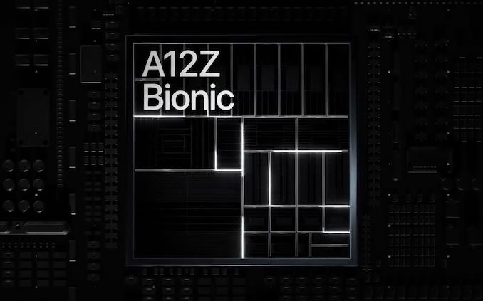
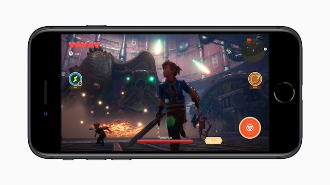
In terms of hardware, the new 2020 iPhone SE is powered by Apple’s latest A13 chip. Currently this is the most powerful and power efficient mobile chip on the market, and Apple integrating this into the new generation SE probably results in the phone packing quite a punch for its size.


Connectivity wise, it’s also on par with the iPhone 11, featuring “gigabit-class” LTE-A cellular as well as the newest WiFi 6 chipsets for better reception on crowded compatible networks.


We currently don’t have information on the DRAM configuration of the phone, but hopefully Apple doesn’t differ it too wildly from the 4GB standard setup on the iPhone 11 models.


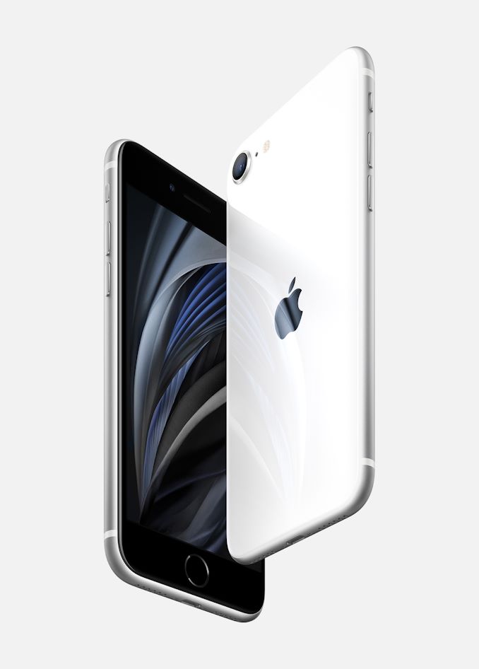
Design-wise, the new iPhone SE should be a very familiar sight to users as it adopts the iPhone 8 design language and frame. This includes a 4.7” 1334 x 750 resolution LCD panel – which in likelihood will be the same as that found on the iPhone 8.


The form-factor nowadays would seem outright diminutive as the phone is smaller in every dimension, coming in at only 138.4 x 67.3 x 7.3mm and weighing in only 148g. If you’ve been looking to get a smaller phone and are in the iPhone ecosystem, the new iPhone SE is the device to get.


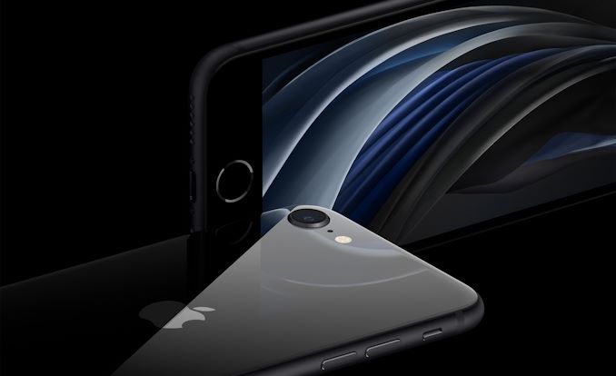
On the camera side, the SE only has a single camera – a 12MP sensor with f/1.8 optics and OIS. This isn’t the newer generation sensor found on the iPhone 11 series as it lacks the full-sensor dual-pixel phase detection capability, so it’s likely the unit from the previous XS and iPhone 8 generation. However this doesn’t mean that picture quality will be any less, as Apple promises the phone to perform as the “best single-camera system ever in an iPhone”, and the A13’s new ISP and image processing algorithms will certainly augment the camera to be extremely competitive with what we’ve seen in the iPhone 11 series.


As the phone still features a physical home button, the preferred method of unlocking is Touch ID as the phone lacks the relevant Face ID sensor hardware. Again, iPhone users will be extremely familiar with the setup here as it’ll be essentially the same as what’s found on an iPhone 8.


A Product That Speaks For Itself – Starting At $399


All in all, the iPhone SE is a product that essentially speaks for itself. It’ll be fulfilling the nostalgia needs of users who had been apprehensive to move onto Apple’s newer “iPhone X” design iteration of phones, all whilst updating the internal hardware of the phone in order to not be left out of the generational technology improvements seen by the newest silicon.  


It also represents amongst the smallest phones on the market right now – you’d have a very hard time finding similar form-factor smartphones, yet alone iPhones.


Apple’s aggressive pricing of starting at $399 for the 64GB base model is going to make this phone a runaway success, even undercutting the iPhone 8 that had been selling for $449 until now (and has now been discontinued). Even the higher storage variants at 128 and 256GB seem outright reasonable at $449 and $549, undercutting the iPhone 11 by $300. European prices start at £419 in the UK and 479€ in continental Europe – a 10% premium on top of the usual VAT margin, so not quite as an aggressive pricing scheme as in the US.


Pre-orders start this Friday, April 17th, with in-store availability next Friday, April 24th.


Source: AnandTech – Apple Announces New Updated iPhone SE: A13 & New Features for 9

XPG Spectrix D50 Memory: A More Subtle RGB DDR4

ADATA’s XPG division has unveiled its latest addition in the high-performance DRAM segment, the Spectrix D50. Starting from 8 GB DDR4-3000 modules, the latest Spectrix D50 kits will go up to 32 GB capacity, with some capacities hitting speeds of up to DDR4-4800.


XPG is the gaming division of ADATA, and has a broad portfolio of DRAM catering to multiple areas on the market. The latest from XPG is the Spectrix D50 which is similar to the Spectrix D60G, but with a more subtle take on RGB. Designed for enthusiasts and overclockers, it has a solid heatsink design with some interesting tweaks to make it look less aggressive than the D60G.


The heat spreader on the Spectrix D50 memory includes a criss-cross geometric design on its 2 mm thick heatsink and a triangular RGB panel that can be controlled via the XPG RGB Sync app. XPG claims it can be used with major motherboard manufacturers own software, but it doesn’t officially state which. Users can customize the look with three available RGB presets which consist of static, breathing, comet, or even synchronize the effect to the sound of music. 


The XPG Spectrix D50 will be available in single 8 GB modules and 2 x 8 GB (16 GB) up to DDR4-4133, with single 16 GB modules and 2 x 16 GB kits ranging up to DDR4-3600. Each kit itself varies in latency from CL16 on the DDR4-3000 and DDR4-3200 kits, with CL18 on the DDR4-3600 kits, each with an operating voltage of 1.35 V.


The higher speed DDR4-4133 kits are CL19 with a higher operating voltage of 1.4 V. All of the XPG Spectrix D50 kits support the latest Intel and AMD platforms through its integrated XMP 2.0 profiles. 


All the XPG Spectrix D50 kits from DDR4-3000 to DDR4-4133 will start filtering into retail channels imminently, with the higher capacity 32 GB modules and the higher speed DDR4-4600/DDR4-4800 kits coming later on in Q2. XPG hasn’t unveiled any pricing information at present.


Related Reading


Source: AnandTech – XPG Spectrix D50 Memory: A More Subtle RGB DDR4

Honor Launches Honor 30 Series in China: Three New Premium Devices

Today Honor completed its Chinese launch of the new Honor 30 series of smartphones, adding three new devices to its premium to flagship line-up of devices. All the new phones are 5G capable and inherit the leading edge custom RYYB camera sensors from Sony that made Huawei devices stand out from the crowd – all in new sleek designs that significantly raises Honor build quality compared to previous generations.


Source: AnandTech – Honor Launches Honor 30 Series in China: Three New Premium Devices

ADATA's New 32 GB DDR4-3200 SO-DIMM, Ideal for Ryzen Mobile

ADATA, one of the leading manufacturers of DRAM and NAND products, has just unveiled its latest memory modules. The new ADATA DDR4-3200 32 GB parts are available in both UDIMM and SO-DIMM format with an operating voltage of just 1.2 V. This is just the ticket for adopters of the new Ryzen 4000 Mobile platform looking to run high-capacity memory without compromising on throughput performance. 


Back at Computex 2019, ADATA showed off its DDR4-2666 SODIMMs for the desktop market. Fast forward to now and it looks to push performance even higher with its new 32 GB DDR4-3200 modules. 


Touching more on the design, we know the ADATA DDR4-2666 modules we saw at Computex were using Micron 16 Gb ICs to build its 32 GB UDIMMs. It is unlikely that ADATA has changed this, but we can’t confirm this at present. The lower operating voltage over conventional DDR3 at 1.5 V according to ADATA equates to around 20% less power being drawn, which in turn generates less heat. 


Potential use cases for DDR4-3200 32 GB memory is in platforms such as AMD’s Threadripper 3000 with a total capacity of 256 GB over eight memory slots. This is more interesting when it comes to mobile platforms such as Ryzen 4000 which has seemingly raised the bar for computational performance in consumer notebooks. Being able to equip a chip with DDR4-3200 helps performance, even if the laptop has a discrete GPU.


In terms of pricing, the new ADATA DDR4-3200 32 GB modules are set to retail with an MSRP of $160. These will filter into retail channels such as Amazon, but they will also be available to purchase from ADATA directly.


Related Reading


Source: AnandTech – ADATA’s New 32 GB DDR4-3200 SO-DIMM, Ideal for Ryzen Mobile

Tyan Updates Transport HX Barebones To Support AMD EPYC 7F32 CPU

Alongside today’s launch of AMD’s new EPYC 7F32, 7F52, and 7F72 processors, stalwart server motherboard and chassis vendor Tyan has officially announced their support for the new chips. Complimenting AMD’s announcements, Tyan is adding support for the chips to select models of their Transport HX barebones servers, which are designed for high-performance computing and server data-driven workflows.


On the back of a new range of EPYC 7002 processors focused on higher core frequency, Tyan has added support to three models. This includes the Tyan Transport HX TN83-B8251, the TS75A-B8252, and the TS75-B8252. Each model follows a 2U2S design for rack mounting and is offered in barebones form with dual SP3 sockets. 


The Tyan Transport HX TN83-B8251 officially supports the new AMD EPYC 7F32, AMD’s 8 core, 180 W TDP chip with base clock of 3.7 GHz and a maximum turbo of 3.9 GHz. The TN83-B8251 comes barebones style inside a TN83 chassis, offering sixteen memory slots with support for DDR4 ECC RDIMM/LRDIMM, as well as 3DS RDIMM/LRDIMM memory with speeds of up to DDR4-3200, for up to 4 TB of capacity. On the Tyan S8251GM2NE-2T motherboard is an Intel X550-AT2 dual 10 G Ethernet controller, with a dedicated Realtek IPMI Ethernet port, and an Aspeed AST2500 BMC.


Tyan TN83-B8251 2U 4-GPU HPC Server


Storage-wise, there is support for up to ten SATA drives via two Slim SAS ports and eight NVMe ports with four SFF-8654 Slim SAS connectors. For graphics cards, there are four full-length PCIe 4.0 x8 slots, with two HH/HL PCIe 4.0 x16 slots which are available with included riser cards. 


Also launched is the Transport TS75A-B8252 and TS75-B252, which both come with a TS75A 2U rackmount chassis and have ten PCIe 4.0 slots. Some of the main features include an Intel X550-AT2 dual 10 G Ethernet controller, an Aspeed AST2500 BMC with Redfish support, which uses a Realtek IPMI Ethernet port. Also included on the S8252GM2NE-2T motherboard is ten PCIe 4.0 slots with three full-length, one PCIe 4.0 x16 OCP 3.0 slot, with the rest accessible via pre-installed riser cards. Both include thirty-two memory slots with support for up to 8 TB of DDR4-3200 ECC memory, with support for RDIMM, LRDIMM, and 3DS modules. 


Tyan Transport HX TS75A-B8252 Rackmount 2U2S Barebones


The only difference between the two B8252 models is through the level of storage support offered. The TS75A-B8252 has twenty-six 2.5″ SATA bays, with twenty-four SATA drives coming from four SFF-8654 connectors, and two regular SATA powered by a Marvel 9235 SATA controller. There are also two NVMe PCIe 3.0 M.2 slots. The TS75-B8252 has twelve 3.5″ SATA bays, with four NVMe U.2 ports which can be used in the bays as well. 


Each model offers its own benefits for the server, data center, and high-frequency trading systems. The new AMD EPYC 7002 7F32, 7F52, and 7F52 feature higher core frequencies, with higher boost frequency capabilities, with the 7F52 offering the highest core-to-cache ratio of any x86 processor on the market.


At present, Tyan hasn’t announced when each of the three new models will be available to purchase, or how much they might retail for.


Related Reading


Source: AnandTech – Tyan Updates Transport HX Barebones To Support AMD EPYC 7F32 CPU

OnePlus Announces OnePlus 8 & OnePlus 8 Pro: Step-Up 2020 Flagships

As the world is in quarantine, smartphone companies aren’t standing still and are still moving forward with their new product launches. We’ve seen almost every other company on the market release their 2020 flagships – but one important vendor has been missing from the line-up: OnePlus. Today, the company is finally revealing its newest OnePlus 8 and OnePlus 8 Pro phones, offering improvements and technology advancements at the highest levels.

Particularly the new OnePlus 8 Pro seems to be the company’s most prestigious flagship device ever, including a new QHD+ 120Hz display, a new generation 1/1.7” camera sensor from Sony along with interesting ultra-wide angle and telephoto modules, the company’s first time adoption of wireless charging – all new features on top of the existing ones that made the OnePlus 7 Pro a great phone in 2019.


Source: AnandTech – OnePlus Announces OnePlus 8 & OnePlus 8 Pro: Step-Up 2020 Flagships

AMD’s New EPYC 7F52 Reviewed: The F is for ᴴᴵᴳᴴ Frequency

Everyone wants a fast processor. The ability to get more stuff done is one of a number of guiding principles of business. However, business also needs consistency, safety and security, which is why having enterprise-class processors is often a requirement in the back-end infrastructure. These processors, with lots of cores, aren’t as fast as consumer processors, so it becomes a tussle whether it makes sense to go fast without security, or to play it safe with a proven platform. With AMD’s new 7F processors, the aim is to provide that proven platform with super-fast cores with lots of cache. We’ve got the 7F52 in for testing today.


Source: AnandTech – AMD’s New EPYC 7F52 Reviewed: The F is for ᴴᴵᴳᴴ Frequency

Apple’s A12Z Processor Confirmed to Reuse A12X Silicon

Last month Apple introduced its latest generation of iPad Pro tablets, and much to the surprise of many, the new iDevices didn’t come with a high-end variant of Apple’s newest A13 SoC. Instead, the iPads used an SoC that Apple was calling the A12Z, clearly indicating that it was based on the same Vortex/Tempest architecture as the earlier A12X, which was used in the 2018 iPad Pros. The unusual move from Apple left us suspecting that the A12Z may not have even been a new chip, but rather a new bin of the A12X, and today we finally have confirmation of that theory thanks to TechInsights.


In a brief tweet, the technical analysis and reverse engineering firm published a note announcing their findings, along with side-by-side die shots comparing A12Z and A12X. In short, the two chips are seemingly identical, with every last functional block in exactly the same place and the same size on A12Z as it was A12X.


While TechInsights’ die shot analysis doesn’t suss out some finer details such as chip steppings – whether A12Z is even on a newer stepping, or if it’s the same stepping as the A12X that Apple was shipping in 2018 for the IPad Pro launch – it’s clear that in terms of silicon, A12Z doesn’t bring anything new to the table.


Instead, the notable changes between the two chips is in their binning/configuration: whereas the A12X only ever shipped with 7 of its GPU clusters enabled, A12Z ships with all 8 enabled. And while a small change in the grand picture of things, it makes sense for Apple to finally enable the 8th cluster for a bit more performance. A12X is produced on TSMC’s 7nm line, and when it was released in 2018, it was one of the biggest 7nm chips being churned out. So Apple should be enjoying much better yields 18 months later, reducing the need to bin to a lower spec to salvage chips.


Apple SoC Comparison
  A12Z A12X A13 A12
CPU 4x Apple Vortex

4x Apple Tempest
4x Apple Vortex

4x Apple Tempest
2x Apple Lightning

4x Apple Thunder
2x Apple Vortex

4x Apple Tempest
GPU 8-cluster, A12-gen 7-cluster, A12-gen

(+ 1 disabled)
4-cluster, A13-gen 4-cluster, A12-gen
Memory Bus 128-bit LPDDR4X 128-bit LPDDR4X 64-bit LPDDR4X 64-bit LPDDR4X
Manufacturing Process TSMC 7nm (N7) TSMC 7nm (N7) TSMC 7nm (N7P) TSMC 7nm (N7)

As for why Apple would opt to re-use A12X for their 2020 tablets instead of commissioning an A13X, while we can only speculate, it almost certainly comes down to economics, as the tablet market is quite different from the smartphone market. Apple is virtually unchallenged as far as high-performance Arm tablets go, and even then, the number of iPads they sell has always been a drop in the bucket compared to the number of iPhones they sell. So there are fewer devices to aromatize the costs of chip development against, and all the while chip development costs are continuing to rise with each new generation of photolithography technology. In short, at some point it has to stop making sense to create new chip designs on a yearly basis for mid-volume products, and Apple may very well have finally hit that mark with their tablet SoCs.


Source: AnandTech – Apple’s A12Z Processor Confirmed to Reuse A12X Silicon

China Develops High Capacity QLC 3D NAND: YMTC at 1.33 Tb

Yangtze Memory Technologies Co. (YMTC) has announced that it’s developed its new 128-layer 1.33 Tb QLC 3D NAND memory chip, the X2-6070. The new chip is based on its Xtacking architecture which enables it to run with super high I/O while maximising the density of its memory arrays. YMTC has also unveiled its plan for a 128-layer 512 Gb TLC chip, the X2-9060, designed to meet more diverse application requirements.


We first reported on the China-based company YMTC entering its 3D NAND memory chips into production back in 2018, when it unveiled its Xtacking Architecture at the Flash Memory Summit. While it didn’t disclose technical details of its announcement, it did state the Xtacking architecture has the capability to run the I/O with speeds of up to 3 Gbps. Fast forward to 2019, and it announced that it planned to start volume production of its 64-layer 3D NAND which we also reported on.


Using its Xtacking architecture at the forefront of production, both the new X2-6070 and X2-9060 feature its updated 2.0 variant which YMTC claims to bring more benefits to flash memory. Both the X2-6070 and X2-9060 are claimed to deliver up to 1.6 Gb/s of I/O performance and operate with a Vccg voltage of 1.2 V. YTMC has stated that the X2-6070 QLC based chip will be first used in consumer-grade SSDs, with the aim to then deliver its capabilities into Enterprise focused drives.


YMTC X2-6070 128-Layer QLC 3D NAND memory chip


The QLC based X2-6070 has 128-layers and more than 366 billion effective charge-trap memory cells. Each memory cell has 4-bit of data, which equates to 1.33 Tb of storage capacity. Everything is proportionate to cost, and it seems like YMTC, which is newer than most to 3D NAND stacking, could again improve its Xtacking architecture in the future.


We expect that YMTC, who is part of the Tsinghua Unigroup in China, is using the XMC fab in Wuhan China to produce its wafers for its 3D NAND. Tsinghua acquired XMC back in 2016, and while we haven’t had it confirmed, it is likely to be producing its wafers at the XMC fab, which is one of China’s largest semiconductor fabrication plants which also uses the Xtacking architecture.


YMTC hasn’t released official specifications or data sheets about the X2-6070 QLC and X2-9060 MLC memory chips, nor has it stated when it is likely to be integrated with its controller partners (or which controllers support it).


Related Reading


Source: AnandTech – China Develops High Capacity QLC 3D NAND: YMTC at 1.33 Tb

ASUS Launches An Old GPU: The NVIDIA GT 710 with Four 4K HDMI Ports

I’ve noticed of late that certain companies are ‘relaunching’ older parts in new designs. We’ve seen it recently with some of the older AMD APUs finding their way into new motherboard designs, but here it’s a case of a base GPU returning to the market. ASUS has listed on its website a ‘new’ GT 710: this is a super low end graphics chip with 192 CUDA cores on the 87 mm2 GK208 Kepler die that originally launched in late 2015 / early 2016. The goal of this sort of graphics card us to supply basic video outputs to machines that do not come with any integrated graphics on the processor.


What’s different about this card, which comes with 2 GB of GDDR5 memory, is that it has four HDMI video outputs. On a modern graphics card you might expect a DisplayPort or two, but here it’s all just HDMI. Despite the GK208 GPU not supporting HDMI 2.0 natively, this is the sort of card that is going to take advantage of NVIDIA opening up 4K60 with 4:2:0 subchroma sampling support on Kepler, which makes it useful for video at the most (you won’t want to be running a full desktop experience with it).


ASUS states that the card can support 4K60 in this mode when one monitor is attached, or 4K30 when multiple displays are attached. Obviously with this horsepower we’re not going to be doing any gaming – it’s simply at the cheap end of the spectrum for office machines or library machines or similar. ASUS suggests using multiple cards at once for anyone that needs 12-16+ displays.


This card uses a PCIe 2.0 x1 connection, ensuring compatibility for a wide range of older machines, and offers a 954 MHz engine clock and a 5000 MHz memory clock. The GT710-4H-SL-2GD5 is expected to be in the ~$50 range when it comes to market.


Source: FanlessTech, ASUS


Related Reading


Source: AnandTech – ASUS Launches An Old GPU: The NVIDIA GT 710 with Four 4K HDMI Ports

EVGA Announces GeForce RTX 2070 Super KO & RTX 2080 Super KO

Expanding its series from its first KO graphics card in years, EVGA unveiled its GeForce RTX 2060 KO at CES 2020, which made waves as was one of the first non-reference GTX 2060 cards to be released at $299. Continuing to fight the good fight for users looking for value from within the latest models, EVGA has released two new models in its KO series, the GeForce RTX 2070 Super KO, and the GeForce RTX 2080 Super KO. 


Back at CES 2020, EVGA released its first KO series card since the GeForce 9800 GTX era with the ray-tracing enabled GeForce RTX 2060 KO. The primary aim was on offering users a card with many of EVGA’s bells and whistles, but at a solid entry-level price point. Building on that, the new EVGA GeForce RTX 2070 Super KO and RTX 2080 Super KO follows on as the successor to the equally good value for money EVGA GeForce RTX Black models.


Some of the most prominent features of the new EVGA RTX Super KO models include a dual-slot, dual-fan cooler, with both models following the same black-themed design of the Super Black Gaming series. And, in what seems like a welcome rarity these days, there is no RGB LED lighting of any kind, which some users may prefer.


Opening up with the beefier of the two cards, the EVGA GeForce RTX 2080 Super KO has the same specifications as the RTX 2080 Super Founders Edition. This includes a base GPU clock speed of 1650 MHz, with a boost clock of 1815 MHz. Memory speeds remain the same at 15.5 Gbps, and the same 8 GB of GDDR6 over a 256-bit memory bus.


The cheaper EVGA GeForce RTX 2070 Super KO also shares the same specifications its reference counterpart, the RTX 2070 Founders Edition. This means the RTX 2070 Super KO has an effective memory clock of 14 Gbps, a base core clock of 1605 MHz which boosts to 1770 MHz. 


Both models share the same design throughout, with its dual-slot twin fan cooler, albeit bereft of a backplate for visually appealing aesthetics and extra cooling on the rear of the cards VRMs. Looking to the I/O, both share the same set of outputs including triple DisplayPort 1.4 outputs, with a single HDMI 2.0b video output. On paper, the only major difference in performance between the new Super KO and Founders Edition models is the custom cooler, with EVGA employing a fairly similar design overall to NVIDIA’s.


The EVGA GeForce RTX 2080 Super KO has an MSRP of $699 with a $10 rebate available to bring it in line with reference model pricing. Cheaper still is the GeForce RTX 2070 Super KO which is available for $499 with users also able to benefit from a $10 instant rebate from EVGA. Both models can be purchased directly from the EVGA online store, or at Amazon and Newegg. 


Related Reading


Source: AnandTech – EVGA Announces GeForce RTX 2070 Super KO & RTX 2080 Super KO

Rebranded Ethernet Technology Consortium Unveils 800 Gigabit Ethernet

With an increasing demand for networking speed and throughput performance within the datacenter and high performance computing clusters, the newly rebranded Ethernet Technology Consortium has announced a new 800 Gigabit Ethernet technology. Based upon many of the existing technologies that power contemporary 400 Gigabit Ethernet, the 800GBASE-R standard is looking to double performance once again, to feed ever-hungrier datacenters.


The recently-finalized standard comes from the Ethernet Technology Consortium, the non-IEEE, tech industry-backed consortium formerly known as the 25 Gigabit Ethernet Consortium. The group was originally created to develop 25, 50, and 100 Gigabit Ethernet technology, and while IEEE Ethernet standards have since surpassed what the consortium achieved, the consortium has stayed formed to push even faster networking speeds, and changing its name to keep with the times. Some of the biggest contributors and supporters of the ETC include Broadcom, Cisco, Google, and Microsoft, with more than 40 companies listed as integrators of its work. 


800 Gigabit Ethernet Block Diagram


As for their new 800 Gigabit Ethernet standard, at a high level 800GbE can be thought of as essentially a wider version of 400GbE. The standard is primarily based around using existing 106.25G lanes, which were pioneered for 400GbE, but doubling the number of total lanes from 4 to 8. And while this is a conceptually simple change, there is a significant amount of work involved in bonding together additional lanes in this fashion, which is what the new 800GbE standard has to sort out.


Diving in, the new 800GBASE-R specification defines a new Media Access Control (MAC) and a Physical Coding Sublayer (PCS), which in turn is built on top of two 400 GbE 2xClause PCS’s to create a single MAC which operates at a combined 800 Gb/s. Each 400 GbE PCS uses 4 x 106.25 GbE lanes, which when doubled brings the total to eight lanes, which has been used to create the new 800 GbE standard. And while the focus is on 106.25G lanes, it’s not a hard requirement; the ETC states that this architecture could also allow for larger groupings of slower lanes, such as 16×53.125G, if manufacturers decided to pursue the matter.


The 800 GbE PCS Flow Diagram


Focusing on the MAC itself, the ETC claims that 800 Gb Ethernet will inherit all of the previous attributes of the 400 GbE standard, with full-duplex support between two terminals, and with a minimum interpacket gap of 8-bit times. The above diagram depicts each 400 GbE with 16 x 10 b lanes, with each 400 GbE data stream transcoding and scrambling packet data separately, with a bonding control which synchronizes and muxes both PCS’s together.


All told, the 800GbE standard is the latest step for an industry as a whole that is moving to Terabit (and beyond) Ethernet. And while those future standards will ultimately require faster SerDes to drive the required individual lane speeds, for now 800GBASE-R can deliver 800GbE on current generation hardware. All of which should be a boon for the standard’s intended hyperscaler and HPC operator customers, who are eager to get more bandwidth between systems.


The Ethernet Technology Consortium outlines the full specifications of the 800 GbE on its website in a PDF. There’s no information when we might see 800GbE in products, but as its largely based on existing technology, it should be a relatively short wait by datacenter networking standards. Though datacenter operators will probably have to pay for the luxury; with even a Cisco Nexus 400 GbE 16-port switch costing upwards of $11,000, we don’t expect 800GbE to come cheap.


Related Reading


Source: AnandTech – Rebranded Ethernet Technology Consortium Unveils 800 Gigabit Ethernet

AMD’s Mobile Revival: Redefining the Notebook Business with the Ryzen 9 4900HS (A Review)

At every turn in the story of AMD’s notebook portfolio, we’ve been there to document the highs and lows. Five years ago, AMD was definitely suffering from a combination of a poor platform, and poor notebook designs tailored for the budget end of the market. Last year, AMD scored a design win in the Microsoft Surface, and now 2020 is set to be another significant step back into this market, with the new Ryzen Mobile 4000 series. Touting over 100+ design wins this year for the new 7nm processor line, we have the first of the halo products in for review: the ASUS Zephyrus G14, with an 8-core Ryzen 9 4900HS under the hood. We’re comparing it to an equivalent Razer Blade 15-inch, and it is very clear that AMD can take the lead in a lot of tests, and be very competitive in others.


Source: AnandTech – AMD’s Mobile Revival: Redefining the Notebook Business with the Ryzen 9 4900HS (A Review)

Samsung Announces Galaxy A51 5G & A71 5G Mid-Range Smartphones

Yesterday Samsung announced the company’s new Galaxy A51 5G and A71 5G phones – for the first time adding 5G capabilities to the company’s arguably most popular and successful phone line-up.


While there’s a lot of talk about the prestige high-end Galaxy S series from Samsung – the majority of phones the company actually sells lies in their more affordable mid-range line-up. Particularly in the last few years, the A-series devices have seen a large amount of success and being Samsung’s top selling phones. The new A51 and A71 iterate on last year’s models – updating a lot of the aspects of the phones hopefully without breaking the bank in terms of cost. Today’s A51 5G and A71 5G phones augment the previously announced A51 and A71’s with 5G connectivity.


Samsung Galaxy A51 & A71 Series
  Galaxy A51 5G Galaxy A71 5G
SoC Exynos 980

2x Cortex-A77 @ 2.2GHz

6x Cortex-A55 @ 1.8GHz


Mali-G76MP5

Display 6.5-inch 6.7-inch
SAMOLED

FHD+ 2400 x 1080 (20:9)
Dimensions 158.9 x 73.6 x 8.7 mm

187 grams
162.5 x 75.5 x 8.1 mm

185 grams
RAM 6/8GB
NAND

Storage
128 GB

+ mSD
Battery 4500mAh (17.32Wh) typ.

4370mAh (16.82Wh) rated
15W

Fast Charging
25W

Fast Charging
Front Camera 32MP

f/2.2
Primary Rear Camera 48MP

f/2.0
64MP

f/1.8
 
Secondary

Rear Camera
12MP Ultra-Wide-Angle

f/2.2
Tertiary

Rear Camera
5MP Depth Camera

f/2.4
Extra

Camera
5MP Macro Shot

f/2.4
4G / 5G

Modem
Exynos 5G – (Integrated)


(LTE Category 16/18)

DL = 1000 Mbps

5x20MHz CA, 256-QAM

UL = 200 Mbps

2x20MHz CA, 256-QAM

(5G NR Sub-6)

DL = 2550 Mbps

UL = 1280 Mbps

SIM Size NanoSIM + eSIM
Wireless 802.11a/b/g/n/ac

BT 5.0 LE, NFC, GPS/Glonass/Galileo/BDS
Connectivity USB Type-C
Special Features On-screen fingerprint sensor
 
Launch OS Android 10 with Samsung OneUI 2.0
(Unconfirmed yet)
Launch Prices n/a n/a

While we don’t have outright confirmation from Samsung, the phones are seemingly powered by the new premium Exynos 980 SoC from Samsung SLSI – it’s the only chip that fits Samsung’s higher-level specifications of the new phone’s SoCs. The chipset was released last September and seemed extremely competitive in its positioning, brandishing all the capabilities of similar chips in its range, including the newest Cortex-A77 CPU cores.


The key aspect of the phones is that they are 5G capable. Samsung here integrates the modem onto the chip, capable of support sub-6GHz networks (mmWave capability is missing – both due to technical lack of ability and the associated higher costs).


Usually Samsung posts an either/or in the specifications of the SoC of a new device when it differs between regions. Here the specifications are referring to a single chip – it’s going to be interesting to see if this also means that Samsung is going forward with the Exynos chip in the USA – typically a market where the company always preferred to use Qualcomm chips.


The phones come in 6 or 8GB of RAM although Samsung doesn’t specify how this will be chosen as they only list 128GB storage as the only configurable option in that regard. MicroSD card slot is naturally still available for more storage.


On the front, both the A51 and A71 come with 2400 x 1080 FHD+ AMOLED displays- only differing in their diagonal size at 6.5” and 6.7”.


These are actually still quite big phones at 73.6 and 75.5mm widths, both wider than a Galaxy S20+, with the A71 almost matching an S20 Ultra in width. Oddly enough, the smaller A51 is advertised as being the heavier of the two new phones at 187g vs 185g.


Both come with a centre hole-punch camera setup, featuring a 32MP sensor and f/2.2 aperture lens. Samsung’s press renders also show the camera cut-out on the higher-end A71 5G is actually larger than on the small model – also a bit odd.


On the rear camera side, the smaller A51 comes with a 48MP sensor at f/2.0, whilst the A71 has a 64MP f/1.8 main camera unit. Both phones share the specifications on the remaining 3 modules: A 12MP f/2.2 Ultra-Wide-Camera, a 5MP f/2.4 depth camera, and a 5MP f/2.4 macro shot camera.


The rear glass design is glass, but with a more shimmering design effect that’s visually distinct and divided into two halves on the phone.


Samsung hasn’t yet announced official pricing for the new 5G variants of the phones (The A51 and A71 were around 300 $/€ to 400 $/€), but says availability will start throughout the month of April depending on region, subject to 5G availability.


Related Reading:


Source: AnandTech – Samsung Announces Galaxy A51 5G & A71 5G Mid-Range Smartphones

SK Hynix Sampling New PCIe 4.0 96L SSDs, 128L 4D NAND Enterprise SSDs

SK Hynix today announced that they’ve begun sampling new generation enterprise EDSFF E1.L SSDs based on their 128-layer “4D NAND” flash modules, in the form of the new PE8111, as well as for the first time introducing PCIe 4.0 connectivity in its new 96-layer U.2/U.3 form-factor PE8010 and PE8030 enterprise SSDs.


We had expected the new PE8111 eSSD for some time know as we reported about SK Hynix’s plans to introduce such a product last November. The biggest change here is the company’s use of new 128-layer 3D NAND modules that the company dubs as “4D-NAND” because of a new denser cell structure design and higher per-die I/O speeds.


16TB Enterprise EDSFF E1.L SSD


The PE8111 still retains as PCIe 3.0 interface and its corresponding performance characteristics plateau at 3400MB/s sequential reads and 3000MB/s sequential writes – whilst supporting random reads and writes up to respectively 700K and 100K IOPs. Because it’s a long-factor EDSFF E1.L form-factor, storage capacity for the unit falls in at 16TB, and SK Hynix is reporting that they’re working on a 32TB solution in the future.


The new PE8010 and PE8030 come in an U.2/U.3 form-factor and are the company’s first SSDs support PCIe 4.0. The SSDs here still rely on 96-layer NAND modules from the company – but are using an in-house controller chip. Bandwidth here is naturally higher, reaching up to 6500MB/s reads and 3700MB/s write sequentially, with random IOPs falling in at respectively 1100K for reads and 320K for writes.


Power consumption for the new U.2/U.3 drives is actually extremely competitive given their jump to PCIe 4.0 – rising only up to 17W as opposed to their previous generation PCIe 3.0 products which fell in at 14W. This is likely to be attributed to the new generation custom controller, which might be more optimised for low-power compared some or the early third-party 4.0 controllers out there.


The PE8010 and PE8030 are sampling right now with customers – with the PE8111 planned to be sampled in the second half of the year.


Related Reading:


Source: AnandTech – SK Hynix Sampling New PCIe 4.0 96L SSDs, 128L 4D NAND Enterprise SSDs

Mobile Benchmark Cheating: When a SoC Vendor Provides It As A Service

Mobile benchmark cheating has a long story that goes far back for the industry (well – at least in smartphone industry years), and has also been a controversial coverage topic at AnandTech for several years now. I remember back in 2013 where I had tipped off Brian and Anand about some of the shenanigans Samsung was doing on the GPU of Exynos chipsets on the Galaxy S4, only for the thing to blow up into a wider analysis of the practice amongst many of the mobile vendors back then – with all of them being found guilty. 


In recent years however we saw a big resurgence of such methods, particularly from Chinese vendors. The one big difference here however is that there’s always been somewhat of a firewall in our coverage between what a device vendor did, and what chip vendors enabled them to do, and that’s where we come to MediaTek’s behavior over the last few years. In most past cases we always blamed the device vendors for cheating as it had been their mechanisms and initiative – we hadn’t had evidence of enablement by chipset vendors, at least until now.


Source: AnandTech – Mobile Benchmark Cheating: When a SoC Vendor Provides It As A Service

ASUS Updates Chromebook Flip Series With Intel 10th Gen Comet Lake

With the vast majority of vendors updating its notebook portfolios with Intel 10th generation processors, ASUS has added a new model its Chromebook lineup, the Chromebook Flip C436. Two new models are available with Intel’s new Comet Lake CPUs, one equipped with a dual-core Intel i3-10110U, while the other variation comes with a quad-core Intel i5-10210U.


Adding to its ‘premium’ range of Chromebooks, which has models starting from entry-level Intel Celeron variants, the new ASUS Chromebook Flip C436 has a 2-in-1 convertible design. It features a compact 14-inch 1080p touchscreen with its 4-sided NanoEdge display technology. The screen itself has a 360° hinge which allows it to be used in multiple configurations including tablet mode, and as a stand. It’s constructed from magnesium alloy and is available in two colors, transparent silver and aerogel white. 


Looking at the technical specifications, there are two current variations available for purchase from the ASUS Store. The cheaper model comes with an Intel i3-10110U, a PCIe 3.0 x2 128 GB NVMe M.2 SSD, 8 GB of DDR3L memory, and a Wi-Fi 6 wireless interface with BT 5.0 support. The more expensive version of the C436 has an Intel Core i5-10210U quad-core processor, a 512 GB PCIe 3.0 x2 NVMe M.2 SSD, 16 GB of DDR3L memory, and the same Wi-Fi 6 adaptor with BT 5.0 connectivity.


Both models include two USB 3.1 G1 Type-C ports, which both support display and power delivery. Along the top bezel is an HD webcam, with an illuminated chiclet keyboard, and a fingerprint sensor integrated into the power button. For sound, the ASUS Chromebook Flip C436 is using a pair of Harman Kardon stereo speakers, with a 3.5 mm Headphone-out and audio-in combo jack for users looking to use headphones or headsets.


The ASUS Chromebook Flip C436 conforms to Intel’s Project Athena certification with a reported battery life of up to 12 hours. The battery spec stands at 42 WHrs due to its 3S1P 3-cell Li-ion battery. It also weighs just 2.6 lbs and sits as its premium Chromebook model, succeeding the C434 we reported on last year.


It’s one of the most extravagant 2-in-1 Chromebooks on the market at present, with prices starting at $800 for the i3 model, with the i5 model costing $1000. Both are currently available to buy from the ASUS store.


Related Reading


Source: AnandTech – ASUS Updates Chromebook Flip Series With Intel 10th Gen Comet Lake

SteelSeries Acquires A-Volute, Company Behind Nahimic Audio Software

Danish peripherals and gaming headset manufacturer SteelSeries has announced its acquisition of A-Volute, the independent developer of the Nahimic audio software. The Danish manufacturer is looking to take full advantage of A-Volutes’ experience to bolster its audio range, with its Arctis series already established in the gaming headset market.


SteelSeries is no stranger to the peripherals market, with experience spanning over the best part of two decades. The company has seen successful product launches, and its popular products including its World of Warcraft branded gaming mice. So in a bid to boost its audio range which is spearheaded by its premium Arctics range, it has acquired A-Volute.


SteelSeries Arctis Pro Wireless Hi-Fidelity Gaming Headset


A-Volutes’ portfolio is impressive and its software is used by many system integrators, including Dell, GIGABYTE, and MSI. For those unfamiliar with it, the Nahimic audio software allows users to setup various audio enhancements/adjustments via with a control panel application. Among other things, the Nahimic software can provide virtual surround sound mixing, as well as audio equalization settings including bass, treble, and voice when used with a microphone. It remains to be seen how SteelSeries is looking to implement Nahimic into its gaming products, but its Arctis Pro comes with a GameDAC which could shed some light on possible use case scenarios.


The Nahimic 3 Audio Control Panel bundled with the MSI MEG X570 Godlike Motherboard


Current SteelSeries CEO Ehtisham Rabbani said this about its purchase of A-Volute:


“With our award-winning innovations that have redefined the gaming audio experience, and our best-in-class SteelSeries Engine software, bringing A-Volute into the SteelSeries family seemed like a natural fit and we are extremely excited about partnering with Tuyen and his team,” said Ehtisham Rabbani, CEO of SteelSeries. “With their excellence in audio software, they’ll help us improve gamers’ audio experiences even further”.


No details regarding the financials of the transaction have been revealed, but SteelSeries says the deal will close later on this spring.


Related Reading


Source: AnandTech – SteelSeries Acquires A-Volute, Company Behind Nahimic Audio Software

CEVA Announces SensPro – New High Performance Sensor Hub IP

As devices become ever more interconnected and increase their capabilities to sense the world through different kind of sensors, there’s an ever more increasing stream of data that is being created. Naturally, not all of that data is useful, with the vast majority of it being thrown away. To differentiate between useful data and less useful noise, there’s an increasing need for processing power on the part of the brains of newer generation devices.


In the past generally we’d have more simplistic sensors such as microphones or accelerometers being the main data sources, and that’s where we usually know the term of “sensor hub” from – when mobile devices first trying to optimise the handling of smartphone sensors. First these were discrete chips, but later on they have been integrated into SoCs.


As data complexity rises, and as new and more complex sensors types appear, CEVA sees to address the need for higher performance sensor hubs. Today’s announcement is about the new SensPro IP family from CEVA, offering a new IP architecture that leverages the company’s existing IP expertise, combining various processing capabilities and flexibility into one single self-contained product offering.


SensPro is a ground-up design that focuses on maximising power efficiency, combining processing designs that were found in CEVA’s NeuPro designs in terms of ML capabilities, the XM6 image processing prowess, as well as the company’s in-house BX2 scalar DSP microarchitecture which serves as the control unit for the whole new IP.


The idea to combine these elements of what are usually different individual IPs into a single processing block is said to be a first in the industry – hence their calling It the first ever “High performance sensor hub DSP”. The goals here are extremely high in terms of the flexibility of the design and what kind of use-cases it’s meant to be deployed in. Usually we think as smartphone being the first such use-case, but it’s actually more in other areas where a device wouldn’t have as high processing capabilities where we’d see the SensPro have a larger impact in. Quoted are use-cases of robotics, automotive, AR/VR headsets, voice assistants, smart home devices and more importantly new industrial applications where we’re seeing a larger shift to more integrated and smarter automation in areas such as production lines.


Combining scalar and vector processing into one IP, with the ability to also process floating-point operations is quite unique – well you’d think a CPU could do that as well, but here CEVA’s advantages lie in their ability to do all of this extremely efficiently in a low-power design.


From a performance standpoint, the new SensPro is a major architectural upgrade over what was previously offered by familiar IP such as the XM6. CEVA here quoted figures such as 400 GFLOPs of power on a 1.6GHz design target in terms of FP performance, achieved through either 64 32-bit FP MAC operations or 128 16-bit ops. FP capability is said to be important for higher precision arithmetic use-cases where higher dynamic range is required, Radar being one data type that is being brought up in this context.


There’s also the fixed-point vector processing pipelines whose configuration contains up to 1024 8×8 MACs, allowing for up to 3 TOPs 8×8 inferencing. CEVA actually also has an execution mode for binary neural networks and promises here up to 20TOPs inferencing throughput, which is a wild number, but we have to remember that this only to applies to specific models that are able to work with only 2-bits of data.


The IP’s data bandwidth capabilities are actually quite massive, employing a super-wide 2048-bit load unit alongside a 1024-bit store unit, which corresponds to 400GB/s of data ingestion and 200GB/s of output. It sounds like a lot, but we have to remember that the IP would be handling immense data streams coming from a myriad of different sensors.


From a high-level perspective, what’s important to note in the block diagram is the configuration flexibility that the IP offers. Generally, amongst the processing units, the scalar processors as well as one vector processing unit are the minimum configuration of the design. Within a vector unit though things can quite a bit more complicated:


A SensPro VCU consists of different execution units handling either fixed point MACs, floating point MACs, or other specifically dedicated special function units for their specific instructions.


The configurability for customers is even more fine-grained than just choosing the amount and type of units that’s integrated into the IP, in the floating point units for example CEVA also gives one the choice between different throughput designs, with a choice of doubling the single-precision throughput to the optional possibility of doubling throughput again for FP16 operations.


CEVA’s initial IP configurations consists of 3 designs – the SP250, SP500F and SP1000, with each incremental step corresponding to the 8-bit MAC configuration. 


  • SP250 – single vector unit with 256 8×8 MACs targeting imaging, vision, and sound centric applications
  • SP500F – single vector unit with 512 8×8 MACs and 64 single precision floating point MACs targeting SLAM centric applications
  • SP1000 – dual vector units with 1024 8×8 MACs and binary networks support targeting AI centric applications

The SP500F is the only starting design that implements the floating-point execution units and is more targeted towards vision and SLAM use-cases with radar or LIDAR. For consumer electronics we’ll most likely see the SP250 being used in devices such as smartphones, IP cameras and other similar products.


Ran Snir, Vice President of Research and Development at CEVA, commented:


“With the growth in the number and variety of sensors in modern systems, and their substantially different computation needs, we set out to design a new architecture from the ground up to address this challenge. We constructed SensPro as a highly configurable, holistic architecture that could handle these intensive workloads using a combination of scalar, vector processing and AI acceleration, while utilizing the latest micro-architecture design techniques of deep pipelining, parallelism, and multi-tasking. The result is the most powerful DSP architecture ever conceived for sensor hubs and we’re truly excited to work with our customers and partners to bring contextually-aware products to market based on it.”


The IP is targeted for general licensing in Q3 2020 – meaning it’ll be a few years before we see any kind of silicon design-ins and even products with the new IP.


Source: AnandTech – CEVA Announces SensPro – New High Performance Sensor Hub IP

Origin PC Announces EON15-X AMD Gaming Laptop: Putting AMD's Ryzen 9 3900 In a Laptop

Even though AMD has already released its Ryzen Mobile 4000 Series of processors, Origin PC has gone one step further for their new AMD gaming laptop, assuming a machine that uses AMD’s Ryzen 3000 desktop processors. Dubbed the EON15-X AMD, the high-end gaming laptop is available with a choice of three different Ryzen 3000 desktop SKUs, including the 12 core Ryzen 9 3900. And yet even with a desktop class processor, this isn’t a luggable, desktop-type laptop; the 15-inch notebook is only 1.2-inches thick and weighs less than 6 pounds.


Thew new EON15-X AMD is the latest update to Origin PC’s lineup of EON15 gaming laptops, with a specific emphasis on supporting AMD’s Ryzen desktop processors. The EON15-X AMD is in 6, 8, and 12 core configurations, which is perfect for gamers and content creators looking to utilize the multi-core performance of AMD’s 7 nm Zen 2 architecture. This is paired with various memory configurations, with the notebook able to accomodate up to 64 GB of DDR4-2666.


And since this is a gaming laptop, it’s of course equipped with high-end display and GPU options. The EON15-X AMD comes with a 15.6″ 1080p 144 Hz screen which is fitting given current trends in gaming laptops, as we as being a good fit for what resolutions current-generation mobile GPUs can handle. Speaking of GPUs, Origin PC is offering users a choice between an NVIDIA GeForce RTX 2060 6 GB, and a GeForce RTX 2070 8 GB graphics card.


Overall, Origin is offering a fairly comprehensive set of customizations on its official product page. Along with the memory options mentioned earlier, the laptop offers support for up to two M.2 SSDs, and a single HDD bay which can accommodate SATA based drives, resulting in a plethora of storage options. In a maximum configuration, the EON15-X AMD supports up to 2 TB NVMe Gen4 drives, M.2 SATA based 2 TB drives, and up to 4 TB of SATA SSDs which can be configured within the customizer


Origin PC EON15-X AMD Specifications
CPU AMD Ryzen 5 3600 6-Core, 3.6 GHz Base, 4.2 GHz Boost

AMD Ryzen 7 3700X 8-Core, 3.6 GHz Base, 4.4 GHz Boost

AMD Ryzen 9 3900 12-Core, 3.8 GHz Base, 4.6 GHz Boost
GPU NVIDIA GeForce RTX 2060 6 GB Max-P

NVIDIA GeForce RTX 2070 8 GB Max-Q
Display 15.6″ IPS FHD 1080p 144 Hz
Memory Origin Approved DDR4-2400

8 GB (2 x 4 GB)

16 GB (2 x 8 GB)

16 GB (4 x 4 GB)

32 GB (4 x 8 GB)

32 GB (2 x 16 GB)

64 GB (4 x 16 GB)


G.Skill Ripjaws DDR4-2400

16 GB (2 x 8 GB)


Kingston HyperX Impact DDR4-2400

16 GB (2 x 8 GB)

32 GB (2 x 16 GB)

64 GB (4 x 16 GB)


Kingston HyperX Impact DDR4-2666

16 GB (2 x 8 GB)

32 GB (2 x 16 GB)

64 GB (4 x 16 GB)

Storage NVMe Up To 2 TB 

M.2 SATA Up To 2 TB

SATA SSD Up To 4 TB
Networking Intel AX200 Wi-Fi 6 + BT 5.0
Ports 1 x USB 3.2 G2 Type-C (DisplayPort 1.4)

2 x USB 3.1 G2 Type-A

1 x USB 2.0 Type-A

1 x 3.5 mm Phono/Mic

1 x 3.5 mm Mic

1 x HDMI TM Output

1 x Mini DisplayPort 1.4 Output

1 x RJ-45
Battery> 62 Wh Li-ion
Dimensions (WxDxH) 14.2 x 10.1 x 1.2 inches
Weight 5.9 lbs
Price (USD) Starts at $1624

On the connectivity front, the Origin PC EON15-X AMD has plenty to shout about with two USB 3.1 G2 Type-A ports, one USB 2.0 port, and a USB 3.2 G2 Type-C port with DisplayPort 1.4 alt mode functionality. Supporting up to three external screens, including the Type-C DisplayPort 1.4 output, and included Mini DisplayPort 1.4 output, with a single HDMI TM video output also present. Gamers looking for RGB are in luck with a full-size customizable keyboard with integrated RGB LEDs and a touchpad which includes an embedded fingerprint reader for extra security.


The Origin PC EON15-X AMD AMD 


Users with deep pockets can also add a bit of flair to their system, as Origin PC offers painting and customization options for the EON15-X AMD. Its HD UV printing service starts at $149, with a metallic finish starting at $175. Origin PC even offer a custom hydro dipping option which begins at $199. 


The Origin PC EON15-X AMD is currently available from the Origin PC website with prices starting at $1624 for the base model, with the price when fully customized can easily surpass $3400. 


Related Reading


Source: AnandTech – Origin PC Announces EON15-X AMD Gaming Laptop: Putting AMD’s Ryzen 9 3900 In a Laptop