ASRock Industrial 4X4 BOX 8040 and NUC(S) Ultra 100 BOX Series Bring Accelerated AI to Mini-PCs

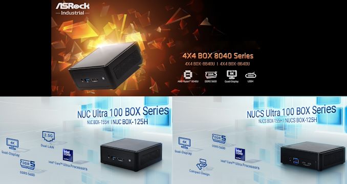
ASRock Industrial maintains a lineup of ultra-compact form-factor machines in the NUC BOX (Intel-based) and 4X4 BOX (AMD-based) series. These systems have gained significant market acceptance (evidenced by the rapid iterations that the company has been able to put out over multiple generations). Being the first to market with the latest platforms has been one of the key reasons behind this.


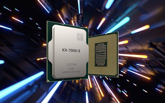
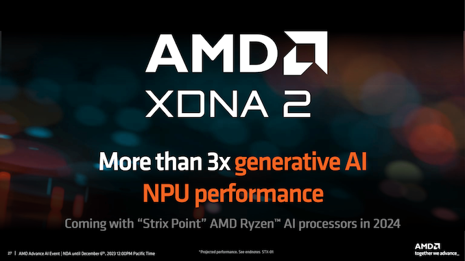
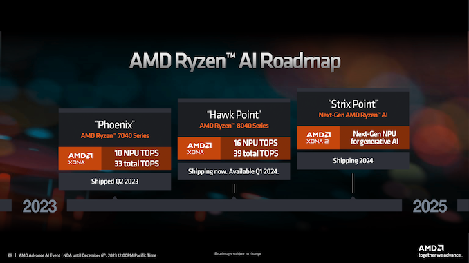
Both Intel and AMD have started to play up hardware-accelerated AI tasks as a key selling point in recent months. Intel has integrated support for NPUs (Neural Processing Unit – the accelerator for neural networks used in machine learning for the tech-savvy folks / artificial intelligence for the average consumer) in the recently-launched Meteor Lake SKUs. AMD’s Phoenix lineup of notebook chips launched earlier this year actually had NPU components on the die in some of the SKUs (AMD’s XDNA). This is now receiving more software support and marketing focus after getting re-branded as Ryzen AI in the recently-launched Phoenix refresh (8040 series APUs).


As is usual for ASRock Industrial, the company was quick to announce their UCFF machines based on both platforms within a few days of the Intel and AMD’s official launch. The 4X4 BOX 8040 Series launch was immediately followed by the introduction of the NUC(S) Ultra 100 BOX Series.


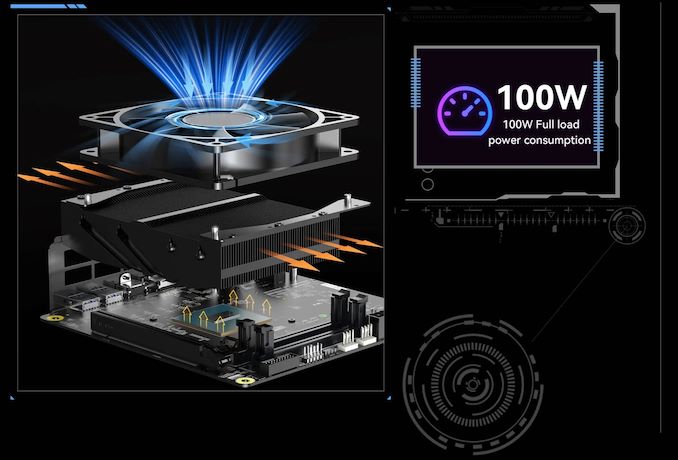
The rich I/O options from the previous generation of 4X4 BOX and NUC(S) BOX are retained as-is, but the key updates are related to the availability of a NPU in the internal platform. On the NUC(S) BOX side, Intel now provides two additional low-power efficiency cores on a separate die in the package. Similar to the previous generation products, the 4X4 BOX 8040 Series and NUC Ultra 100 BOX Series are the thick versions (49mm height). The NUCS Ultra 100 BOX is the 38mm slim version without the 2.5″ SATA drive support and the second LAN port. Each series has multiple processor options at different price points.


ASRock Industrial’s AMD Hawk Point & Intel Meteor Lake UCFF PC Lineup
Model 4X4 BOX 8040 Series NUC Ultra 100 BOX Series NUCS Ultra 100 BOX Series
CPU Options AMD Ryzen 7 8840U

8C / 16T

3.3 GHz (Up to 5.1 GHz)

28W

(4X4 BOX-8840U)

AMD Ryzen 5 8640U

6C / 12T

3.5 GHz (Up to 4.9 GHz)

28W

(4X4 BOX-8640U)
Intel Core Ultra 7 155H

(6P + 8E + 2e / 22T)

1.4GHz / 900MHz / 700MHz (up to 4.8GHz / 3.8 GHz / 2.5 GHz)

28W

(NUC(S) BOX-155H)

Intel Core Ultra 5 125H

(4P + 8E + 2e / 22T)

1.2GHz / 700MHz / 700MHz (up to 4.5GHz / 3.6 GHz / 2.5 GHz)

28W

(NUC(S) BOX-125H)
GPU AMD Radeon 780M

(12 CU / 768 Shaders) @ 2.7 GHz

(4X4 BOX-8840U)

AMD Radeon 760M

(8 CU / 512 Shaders) @ 2.6 GHz

(4X4 BOX-8640U)
Intel Arc Xe

8 Cores @ 2.25 GHz

(NUC(S) BOX-155H)

Inte Arc Xe

7 Cores @ 2.2 GHz

(NUC(S) BOX-125H)
NPU Ryzen AI (up to 16 TOPS) Intel AI Boost @ 1.4 GHz (up to 11 TOPS)
DRAM Two DDR5 SO-DIMM slots

Up to 96 GB of DDR5-5600 in dual-channel mode
Motherboard 10.4 cm x 10.2 cm x 3.6 cm (4.02″ x 4.09″) UCFF
Storage SSD 1x M.2-22(42/80) (PCIe 4.0 x4)

1x M.2-2242 (PCIe 4.0 x4)
1x M.2-22(42/80) (PCIe 4.0 x4)

1x M.2-2242 (PCIe 4.0 x4)
1x M.2-22(42/80) (PCIe 4.0 x4)

1x M.2-2242 (PCIe 4.0 x1)
DFF 1 × SATA III Port (for 2.5″ drive)
Wireless Mediatek MT7922 (RZ616)? Wi-Fi 6E

2×2 802.11ax Wi-Fi (2.4Gbps) + Bluetooth 5.2 module
Intel Wi-Fi 6E AX211

2×2 802.11ax Wi-Fi (2.4Gbps) + Bluetooth 5.3 module
Ethernet 1x 2.5 GbE RJ-45 (Realtek RTL8125)

1x GbE RJ-45 (Realtek RTL8111H)
1x 2.5 GbE RJ-45 (Intel I226-LM)

1x 2.5 GbE RJ-45 (Intel I226-V)
1x 2.5 GbE RJ-45 (Intel I226-LM)
USB Front 1× USB 3.2 Gen 2 Type-A

2x USB4 (with DisplayPort 1.4a)
2× USB 3.2 Gen 2 Type-A

1x USB4 / Thunderbolt 4 (with DisplayPort 2.1)

1x USB 3.2 Gen 2 Type-C (with DisplayPort 1.4a Alt Mode)
Rear 2 × USB 2.0 Type-A 2 × USB 3.2 Gen 2 Type-A
Display Outputs 2 × HDMI 2.1 (Rear, up to 8Kp60)

2 × DisplayPort 1.4a (using Front Panel Type-C ports, up to 4Kp60)
2 × HDMI 2.1 (Rear, up to 4Kp60)

1 × DisplayPort 1.4a (using Front Panel Type-C port, up to 4Kp60)

1 × DisplayPort 2.1 (using Front Panel Type-C port, up to 4Kp60)
Audio 1 × 3.5mm audio jack (Realtek ALC256)
PSU External (19V/120W)

(4X4 BOX-8840U)

External (19V/90W)

(4X4 BOX-8640U)
External (19V/120W)

(NUC(S) BOX-155H)

External (19V/90W)

(NUC(S) BOX-125H)
Dimensions Length: 117.5 mm

Width: 110 mm

Height: 49 mm
Length: 117.5 mm

Width: 110 mm

Height: 38 mm
Product Links 4X4 BOX-8040 Series NUC BOX-100 Series NUCS BOX-100 Series


Note that the M.2 2280 support is enabled by a separate bracket, similar to the previous generation UCFF systems from the company. The Intel platform’s WLAN module seems to have received a slight upgrade from the AX210 to the AX211, which brings in Bluetooth 5.3 support. There is still no sign of Wi-Fi 7 / 802.11be support, but the industry is probably waiting for notebook makers to take the lead. In any case, for industrial PCs, the wired LAN subsystem is more important than the wireless one. The dual RJ-45 ports in most of the new models is a welcome trend from that viewpoint.


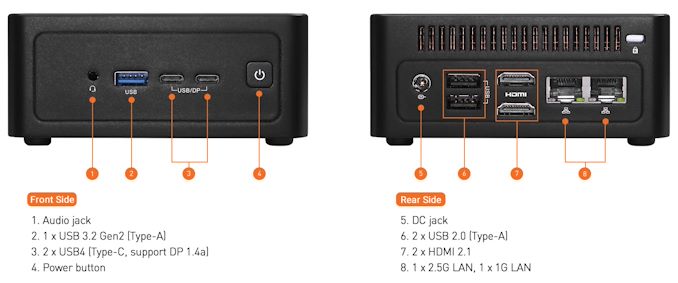
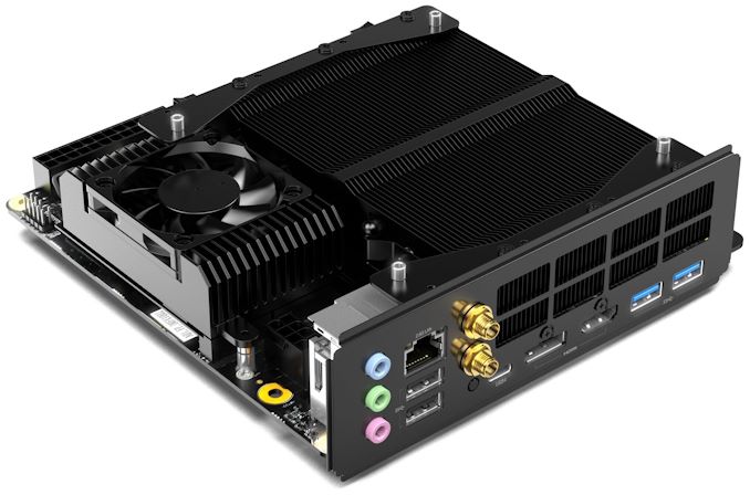
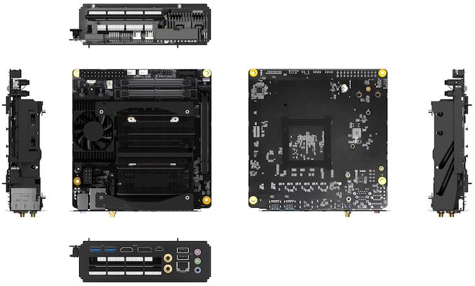
4X4 BOX-8040 Series I/O


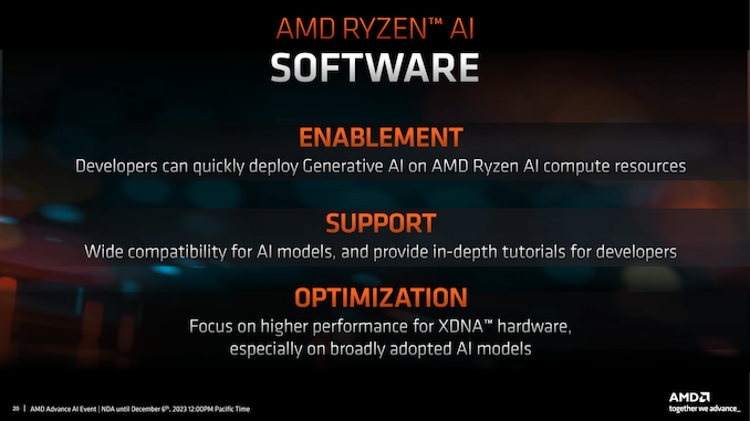
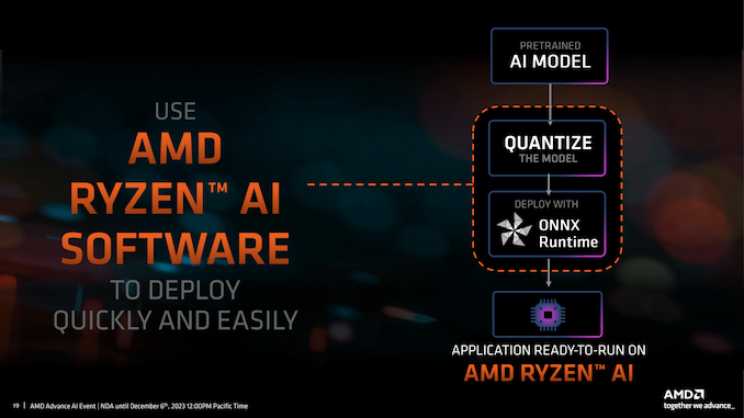
The word on the street right now is that the Arc Xe Graphics in Meteor Lake brings Intel on a competitive footing against the RDNA3-based Radeon 780M in the Phoenix parts. The AI performance claims are more of a mixed bag, because Intel has been pushing a hybrid strategy that includes all of the CPU, GPU, and NPU in accelerating machine learning tasks. AMD’s approach for client platforms is not clear yet beyond the promotion of the new NPU components on the die. Both companies claim to have significant support from software vendors, and that is good news for consumers.


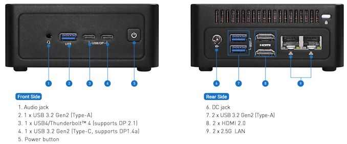
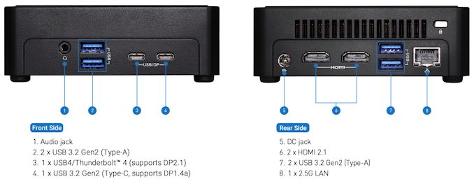
NUC Ultra 100-BOX Series I/O


NUCS Ultra 100-BOX Series I/O


As ASRock Industrial re-uses the case designs and thermal solutions from previous generations for rapid iterations, it takes a few releases before customer feedback gets adopted. The glossy chassis is finally gone from all versions of the products, with the matte design seen in the NUCS BOX-1300 series making its way across the board. We are still worried about the lack of an effective thermal solution for the M.2 NVMe SSDs inside these systems. It remains to be seen in hands-on evaluation if any progress has been made on that front. The other aspect is that the BIOS is usually not power-optimized at launch, but we have seen the company release regular updates even for previous generation products in an effort to address that. Other than these minor nit-picks, the NUC(S) BOX and 4X4 BOX systems from ASRock Industrial have proved to be worthy replacements for the mainstream Intel NUCs. We have reached out to ASRock Industrial for clarity on market availability dates and pricing, and will update the article with the details after receiving them.


Source: ASRock Industrial – 4X4 BOX-8040 Series PR


Source: AnandTech – ASRock Industrial 4X4 BOX 8040 and NUC(S) Ultra 100 BOX Series Bring Accelerated AI to Mini-PCs

ASML Ships Industry's First High-NA EUV Litho Scanner To Intel

ASML on Thursday said that it had shipped its pilot High-NA EUV scanner to Intel. The Twinscan EXE:5000 extreme ultraviolet (EUV) scanner is AMSL’s very first High-NA scanner, and it has eagerly been awaited by Intel, who first placed an order for the machine back in 2018. Intel will be using the new machine to experiment with High-NA EUV before it deploys commercial grade Twinscan EXE:5200 tool for high-volume manufacturing (HVM) sometime in 2025. The announcement represents a major industry milestone that will have an impact not only on Intel, but eventually on the other leading-edge fabs as well.


“We are shipping the first High NA system and announced this in a social media post today,” a spokesperson for ASML said. “It goes to Intel as planned and announced earlier.”


The ASML Twinscan EXE High-NA scanner is set to make its journey from Veldhoven in the Netherlands all the way to Intel’s facility near Hillsboro, Oregon, where the tool, jokingly referred to by Intel CEO Pat Gelsinger as Dr. Ann Kelleher’s Christmas present, will be installed in the coming months. It is quite a colossal piece of equipment – so large, in fact, that it requires 13 truck-sized containers and 250 crates just to transport it. And once assembled, the machine is 3 stories tall, which has required Intel to build a new (and taller) fab expansion just to house it. It is estimated that each of these High-NA EUV scanners comes with a hefty price tag, likely in the range between $300 million and $400 million.


High numerical aperture (High-NA) EUV lithography tools featuring a 0.55 NA lens are capable of an 8nm resolution, which is a significant improvement compared to current EUV tools with a 13nm resolution. These next-generation High-NA EUV scanners are expected to be important for chip production using process technologies beyond 3nm, which the industry is set to adopt in 2025 – 2026, as they will allow fabs to avoid using EUV double patterning, greatly reducing complexity while potentially enhancing yields and lowering costs.


But ASML’s Twinscan EXE lithography tools with a 0.55 NA will be significantly different than the company’s regular Twinscan NXE litho machines with a 0.33 NA. An avid reader will remember from our previous reports that High-NA scanners are going to be significantly bigger than contemporary EUV scanners, which will require new fab structures. But these is by far not the only difference.


Perhaps the biggest change between the High-NA and regular EUV scanners is the halved reticle size of the High-NA scanners, which will require chipmakers to rethink how they design and produce chips – especially at a time when high-end GPUs and AI accelerators are pushing the limits for reticle sizes. In addition, since High-NA scanners will support a higher resolution and different reticle size, they will require new photoresists, metrology, pellicle materials, masks, and inspection tools, just to name some of the alterations. In short, High-NA tools will require significant investments in infrastructure to go with them.


Although semiconductor production infrastructure is developed by the whole industry, the best way to adopt it for real-world production is to tailor it for actual process technologies and process recipes. Which is why it is so important to start working with pilot scanners early to prepare for HVM using production machines.


Intel was the first company to order ASML’s pilot Twinscan EXE:5000 scanner back in 2018. It was also the first to place an order for ASML’s commercial grade Twinscan EXE:5200 litho tool in 2022. The company is set to start development work on its 18A node (18 angstroms, 1.8nm) in 2024 and then will employ High-NA tools for a post-18A node, presumably in 2025 – 2026.


By getting High-NA tools earlier than its rivals, Intel not only be able to ensure that its tools produce desired results, but it has a chance to set the standards for the industry when it comes to High-NA manufacturing. For Intel this might mean getting a significant advantage over its rivals, Samsung Foundry and TSMC.


ASML announced in 2022 that it will be able to produce 20 High-NA EUV litho tools per year in 2027 – 2028. Meanwhile, the company disclosed earlier this year is that it had a double-digit number of machines in its High-NA backlog, which signals that its partners are set to adopt these scanners in the coming years. And leading that pack will be Intel.


Source: AnandTech – ASML Ships Industry’s First High-NA EUV Litho Scanner To Intel

Silicon Power MS70 SSD-in-a-Stick Review: Thumb Drive Meets Massive Capacity

NAND flash technology has seen rapid advancement in recent years. This has resulted in the capacity limits of SSDs and thumb drives getting pushed up regularly. Companies like Kingston had innovated in the late 2010s to deliver 1TB and 2TB thumb drives. They were overpriced and over-sized for their product class at that time. However, interest in this category has been sparked again by the introduction of high-performance native UFD controllers and the appearance of cost-effective high capacity NAND dies. Silicon Power and Transcend recently released 2TB thumb drives based on the Phison U17 and Silicon Motion SM2320 native UFD controllers respectively. Read on for a comprehensive analysis of the performance profile and value proposition of the Silicon Power MS70 in its 2TB avatar.


Source: AnandTech – Silicon Power MS70 SSD-in-a-Stick Review: Thumb Drive Meets Massive Capacity

Apple to Halt Sales of Watch Series 9 and Ultra 2 in the U.S. Due to Patent Dispute

Apple on Monday said it would pause sales of its Watch Series 9 and Ultra 2 in the U.S. due to an ongoing patent dispute. The patents in question cover the blood oxygen feature in the watches, and belong to medical technology company Masimo. Apple itself said it would halt sales of its latest oxygen sensor-equipped smart watches online starting December 21, and in retail starting December 25.


The dispute’s roots lie in Masimo’s claims that Apple’s blood oxygen sensor infringes on 15 of its patents. The ITC ruling, announced in October, upheld a judge’s decision from January and triggered a 60-day Presidential Review Period, which will be expiring on December 25. Despite the possibility of a veto from President Biden, Apple decided to halt sales of its latest smart watches as a proactive measure.


Sales of the affected Apple Watch models will cease on Apple’s website after 3 PM ET on December 21 and in Apple’s retail stores after December 24. Notably, this ban is exclusive to Apple’s direct sales channels; third-party retailers like Amazon and Best Buy can continue selling the devices until December 25. This limited scope of the ban provides a brief window for consumers to purchase these models from alternative sources in time for Christmas.


Behind the scenes, Apple is actively contesting the ruling and exploring various legal and technical options to ensure the continued availability of its watches. The company argues that the ban could adversely affect both consumers and the broader economy, given the significant revenue generated by Apple’s wearables business, especially during the Q1 2023 holiday quarter. Meanwhile, Masimo maintains its stance, viewing the ITC’s ban as a strong message about adhering to patent laws.


The Patent Trial and Appeal Board evaluated 17 Masimo patents, invalidating 15, a decision that Masimo is now contesting. During Masimo’s trade secret misappropriation trial in May, a judge dismissed half of its 10 claims due to insufficient evidence. Of the remaining claims, a majority of jurors sided with Apple, but with one dissenting, they could not reach a unanimous verdict, leading to a mistrial. A date for a new trial has yet to be set.


Currently, there is no defined duration for the unavailability of Apple Watch Ultra 2 and Series 9. While a veto from the Biden administration remains possible, Apple plans to appeal the ITC’s decision with the U.S. Court of Appeals for the Federal Circuit after the Presidential Review Period, starting December 26. This appeal will not postpone the sales and import ban on these models since the disputed Masimo patents are valid until August 2028, but if the court sides with Apple, the company could return its products to the U.S. market. Apple has alternative options, such as negotiating a settlement or a licensing deal with Masimo. Additionally, the company could redesign its smartwatches to bypass the two Masimo patents, possibly by updating Apple Watch’s firmware.


It should be noted that the ITC’s decision is specific to models featuring the blood oxygen monitoring technology. As a result, the Apple Watch SE, which lacks this feature, remains unaffected and will continue to be available.


The ban’s impact is expected to affect Apple’s earnings, yet it does not affect Apple Watches already sold or their functionality. Existing models with the blood oxygen sensor, introduced with the Apple Watch Series 6 in 2020, will continue to operate as usual. Furthermore, the ITC’s order permits service, repair, or warranty work on units sold before December 25.


Sources: Reuters, 9to5Mac.


Source: AnandTech – Apple to Halt Sales of Watch Series 9 and Ultra 2 in the U.S. Due to Patent Dispute

The XPG Core Reactor II 1200W PSU Review: XPG Goes for the Gold

An increasingly common face in the power supply market, the bulk of XPG’s work thus far has been on high-end, high-margin power supplies, such as their 80Plus Platinum-rated Cybercore II. But as the company has become better established in the PSU market on the back of multiple successful products, the company is looking to expand their footprint by venturing into the mid-range segment.

Spearheading that effort is the new XPG Core Reactor II series. Looking to maintain their competitive edge with, what’s frankly, a cheaper power supply design, XPG needs to walk a very tight rope, where where the equilibrium between performance, quality, and cost is crucial. In this category, PSUs must support a range of computing setups while maintaining a focus on value for money. The Core Reactor II series represents XPG’s dedication to this segment, illustrating their capability to cater to a broad spectrum of users who seek a blend of reliable performance and economic viability.

As an 80Plus Gold certified unit and without too many bells and whistles, the Core Reactor II stands out for its practical design, tailored to deliver consistent performance without the premium cost. In examining the details of the XPG Core Reactor II series, we will evaluate how well these PSUs align with XPG’s commitment to affordable quality and whether they meet the diverse needs of mid-range computing environments.


Source: AnandTech – The XPG Core Reactor II 1200W PSU Review: XPG Goes for the Gold

Intel Reiterates: We Are Not Going to Spin Off IFS

When Intel struggled with its 10nm process technology a few years ago, some investors suggested that the company would be better-off spinning its chip production into an independent foundry, leaving the core of the company to focus on chip design instead. Bucking these calls, however, Intel opted to keep chipmaking in-house, even going as far as to creating Intel Foundry Services to use those facilities to do contract chipmaking for other chip designers.


With the significant capital required to scale up the chip fab side of the business, it’s a decision that, even today, Intel executives still get asked about. That was once again the case yesterday, at Intel’s investor-focused AI Everywhere event at the Nasdaq MarketSite, where Intel CEO Pat Gelsinger reiterated that the company is not going to spin off their foundries.


“The idea of the internal foundry model, we think, is the right path for us in the current environment,” Gelsinger told Reuters.


IFS is currently a distinct manufacturing operations unit within Intel that operates like ‘an internal foundry’, which the company then ‘outsources’ production of its processors and other products. Since returning to Intel, Gelsinger has been steadfast about wanting IFS to stay that way, keeping IFS an internal unit rather than to spin it off. It’s a decision that’s been in notable contrast to some other Intel divisions, such as Mobileye and the Programmable Solutions Group, which have been (or will be) spun off into separate businesses.


With that said, Intel will be bringing more transparency to the financials of its foundry division. Starting from Q2 next year, Intel will report financial results of IFS as if it was a separate business, which will give a clear understanding how much the unit earns and provide a better understanding of how IFS operations stack up against those of TSMC, Samsung Foundry, GlobalFoundries and other top contract chipmakers.


Ultimately, Intel believes that there are clear benefits to operating in a unified manner, especially, as explained by Gelsinger in his interview, that Intel is using the majority of the factory’s capacity right now.


Source: AnandTech – Intel Reiterates: We Are Not Going to Spin Off IFS

Intel Releases Core Ultra H and U-Series Processors: Meteor Lake Brings AI and Arc to Ultra Thin Notebooks

Intel has released their first mobile processors based on their highly anticipated Meteor Lake platform, the Core Ultra H and the Core Ultra U series. Available today, the Ultra Core H series has four options, including two Ultra 7 16C/22T (6P+8E) SKUs and two 14C/18T (4P+8E) Ultra 5 SKUs, and offers a base TDP of 28 W, with a maximum turbo TDP of up to 115 W. The Core Ultra-H series is designed for ultra-portable notebooks but offers more performance in both computing and graphics within a slimline package.

Also announced is the Intel Core Ultra U-series, which includes four 15/57 W (base/turbo) SKUs, with two Core Ultra 7 and two Core Ultra 5 SKUs, and all coming with a variance in P, E-core and Intel’s latest integrated Arc Xe graphics frequencies. All of Intel’s announced Core Ultra U-series processors for mobile feature 10C/14T, with two Performance cores and eight efficiency cores, making them ideal for lower-powered and ultra-thin notebooks.

The launch of Intel’s tile-based Meteor Lake SoC marks the first step in a series of power-efficient and AI-focused chips on Intel 4 for the mobile market, which is ultimately designed to cater to the growing need to utilize AI inferencing on-chip. Both the Intel Core Ultra H and U families of chips include two new Low Power Island (LP-E) cores for low insensitive workloads, with two Neural Compute Engines within the Intel AI NPU designed to tackle generative AI inferencing.


Source: AnandTech – Intel Releases Core Ultra H and U-Series Processors: Meteor Lake Brings AI and Arc to Ultra Thin Notebooks

Zhaoxin Unveils KX-7000 CPUs: Eight x86 Cores at Up to 3.70 GHz

Zhaoxin, a joint venture between Via Technologies and Shanghai Municipal Government, has introduced its Kaixian KX-7000 series of x86 CPUs. Based on the company’s Century Avenue microarchitecture, the processor features up to eight general-purpose x86 cores running at 3.70 GHz, while utilizing a chiplet design under the hood. Zhaoxin expects the new CPUs to be used for client and embedded PCs in 2024.


According to details published by Zhaoxin, the company’s latest Century Avenue microarchitecture looks to be significantly more advanced than the company’s previous x86 microarchitecture. This new design includes improvements in the CPU core front-end design as well as the out-of-order execution engines and back-end execution units. The CPU cores themselves are backed by 4MB of L2 cache, 32 MB of L3 cache, and finally a 128-bit memory subsubsystem supporting up to two channels of DDR5-4800/DDR4-3200. Furthermore, the new CPUs pack up to eight cores, capable of reaching a maximum clockspeed of 3.70 GHz.


As a result, the new CPUs are said to double computational performance compared to their predecessors, KaixianKX-6000 launched in 2018.


On the graphics side of matters, Zhaoxin’s Kaixian KX-7000 CPUs also pack the company’s new integrated GPU design, which is reported to be DirectX 12/OpenGL 4.6/OpenCL 1.2-capable and offers four-times the performance of its predecessor. Though given the rather low iGPU performance of the DirectX 11.1-generation KX-6000, even a 4x improvement would make for a rather modest iGPU in 2024. Principly, the iGPU is there to drive a screen and provide media encode/decode functionality, with the KX-7000 iGPU capable of decoding and encode H.265/H.264 video at up to 4K, and can drive DisplayPort, HDMI, and D-Sub/VGA outputs.


Another interesting detail about Zhaoxin’s KX-7000 processors is that the company says they’re using a chiplet architecture, which resembles that of AMD Ryzen’s processors. Specifically, Zhaoxin is placing their CPU cores and I/O functions in to different pieces of silicon – though it’s unclear into how many different chiplets altogether.


On the I/O side of matters, the new CPUs provide 24 PCIe 4.0 lanes, two USB4 roots, four USB 3.2 Gen2 roots, two USB 2.0 root, and three SATA III ports. And, given the target market, it offers acceleration for the Chinese standard SM2 and SM3 cryptography specifications.


At the moment, Zhaxin is not disclosing where it plans to produce its Zhaoxin’s KX-7000 processors, nor on what node(s) they’ll be using. Though given Zhaoxin’s previous parts the and the limited, regional market for the chips, it is unlikely that they’re intending to use a leading-edge fabrication process.


Perhaps the final notable detail about Zhaoxin’s Kaixian KX-7000 CPUs is that they are set to come in both BGA and LGA packages, something that does not often happen to Chinese CPUs. An LGA form-factor will enable an ecosystem of interchangeable and upgradeable chips, which is something that we have not seen from Chinese processors for client PCs in the recent years.


Zhaoxin says that major Chinese machine manufacturers, including Lenovo, Tongfang, Unigroup, Ascend, Lianhe Donghai, and others, have developed new desktop systems based on the KX-7000 processors. These systems – which will be available next year – will run operating systems like Tongxin, Kylin, and Zhongke Fonde.


Source: AnandTech – Zhaoxin Unveils KX-7000 CPUs: Eight x86 Cores at Up to 3.70 GHz

Adata, OWC, and Stardom Roll Out USB4 SSDs and Enclosures for Faster External Storage

When the USB4 specification emerged several years ago, it was quickly positioned as a less expensive alternative to the Thunderbolt 3 technology which ruled the market of high-performance direct-attached storage (DAS) devices and docking stations. Since then, we’ve seen multiple USB4 docks hit the market, but USB4 DASes and SSDs are still rare. Thankfully, the situation began to change in the recent weeks, as multiple vendors have finally begun releasing their own USB4 SSDs and external drive enclosures.


Adata


Adata announced its first SE920 External USB4 SSD back in August 2021, but it only started shipping these drives in October. Adata’s SE920 External SSDs offer capacities of 1 TB or 2 TB, along with a sequential read speed rating of up to 3.8 GB/s as well as a sequential write speed of up to 3.7 MB/s when working with a USB4 host. Otherwise, the drive is rated for 3.20 GB/s on Thunderbolt hosts, due to the greater overhead of the Thunderbolt protocol.


One interesting feature of the Adata SE920 External USB4 SSD is that it comes with a ‘telescoping’ case that allows to activate its internal fan for better heat dissipation. Such design allows to better ensure consistent performance under high loads, which is set to be particularly useful when transferring large volumes of data. Meanwhile, like other modern SSDs, the SE920 uses pseudo-SLC caching, which means that it demonstrates its maximum performance only while there is spare SLC-cache.


Adata’s drive looks like a very decent product overall, and it’s priced very competitively with other high-performance drives on the market, with Adata charging around $150 for the 1 TB version and $200 for the 2 TB version.


OWC


Meanwhile, for the DIY crowd that wants to build their own USB4 SSDs, standalone USB4 enclosures are finally available as well. OWC’s Express 1M2 enclosure is based on the ASMedia ASM2464PD USB4/Thunderbolt to NVMe bridge, and is compatible with virtually any NVMe M.2-2280 SSD.


The enclosure supports sequential read/write speeds of up to 3,151 MB/s, as well as capacities up to 8 TB (the largest M.2 2280 drive capacity currently available). Mindful of how warm modern, high-end SSDs can get, the enclosure’s case acts like a huge heat sink, helping to keep those increasingly toasty SSDs cool.


On paper, OWC’s Express 1M2 DIY enclosure does not reach speeds quite as high as Adata’s SE920 SSD, so the extra capacity and ability to throw in any M.2 SSD you have lying around are the main selling points of the device. Pricing, on the other hand is a higher hurdle; OWC is charging $119.99 for the Express 1M2 enclosure on its own, and $219.99 for the enclosure with pre-installed 1 TB SSD.


Stardom


Although OWC’s DIY USB4 SSD enclosure seems a bit overpriced, good news is that the company is not alone selling such devices. Stardom also has its UBOX-B4BP USB4 SSD enclosure that has the same feature set (e.g., compatibility with almost any M.2-2280 SSD and latest PCs), but it is slightly larger and its rated  performance figures are up to 2,920 MB/s for writes and up to 3,214 MB/s for reads.


The enclosure allows building external USB4 storage solutions of up to 8 TB (and larger when such drives become available) that can work with both new and old PCs. Interestingly, Stardom has included a second USB-C connector on the enclosure solely for power purposes, allowing it to be used with an external power adapter if a host can’t provide enough bus power on its own.


Stardom yet has to start selling its its UBOX-B4BP USB4 SSD enclosure in the U.S. and Europe, but in Taiwan the product costs NT$3,990 ($120 without VAT), which is not exactly cheap.


Sources: Adata, OWC, Stardom


Source: AnandTech – Adata, OWC, and Stardom Roll Out USB4 SSDs and Enclosures for Faster External Storage

HP Z6 G5 A Workstation Review: 96-Core AMD Ryzen Threadripper Pro 7995WX Impresses

With AMD’s recent launch of their Zen 4 architecture-based Threadripper 7000 series CPUs, the company and its OEM partners have unleashed a new wave of high-end PCs and workstations based on the considerable-core-count processors. Though not a massive market in and of itself, the workstation market is by most respects the pinnacle of the PC market, with systems employing the biggest and fastest hardware available, and often a whole lot of it. As a result, the workstation market is still a very important one to PC OEMs and chip vendors who are looking to move big silicon for big prices – but it’s also a fun one for consumers to watch, if only for a glimpse of what all of this PC hardware is capable of in its most powerful configurations.


As Threadripper Pro 7000 workstations are now shipping, we’re finally getting our first look at AMD’s premiere workstation silicon. Unlike AMD’s vanilla Threadripper 7000 processors, which we reviewed last month, for their top-end Pro silicon AMD is letting their OEM partners take the lead in showcasing their latest wares. With virtually all workstation-grade CPUs sold to OEMs, self-built workstations aren’t really a thing. At the same time, good workstation hardware it in a class of its own, not just with chips but with regards to the entire package – and all of which AMD’s OEM partners are eager to show off. Which for today’s review, means we get to do something we don’t get to do very often at AnandTech, and take a look at a proper, high-end workstation.


For our first look at the Threadripper Pro 7000 series hardware, today we are taking a look at a fully-fledged workstation from HP’s Z6 range, the HP Z6 G5 A. The HP Z6 G5 A system we have in for review today includes the Ryzen Threadripper Pro 7995WX with 96C/192T, with 128 GB of DDR5-5200 RDIMM (8 x 32 GB), as well as NVIDIA’s RTX A4000 single-slot graphics card designed for AI-accelerated compute and high-performance real-time ray tracing. With such a high-end specification, we’re putting the HP Z6 G5 A up against Intel’s flagship Xeon W9-3495X (56C/112T) workstation processor and AMD’s non-Pro Ryzen Threadripper 7000 series processors.


Source: AnandTech – HP Z6 G5 A Workstation Review: 96-Core AMD Ryzen Threadripper Pro 7995WX Impresses

Minisforum Launches AR900i: A $559 Core i9-13900HX Mini-ITX Platform

Minisforum has launched a new high-performance Mini-ITX motherboard that’s based on Intel’s 13th Generation Core HX mobile parts. The upsized, highly integrated AR900i platform promises to bring together the power efficiency benefits of a mobile platform with desktop-class performance and features – and all at a rather moderate price.


Minisforum itself calls its AR900i platform an ultimate mobile-on-desktop (MoDT) platform and indeed it is quite capable thanks to its 14-core Core i7-13650HX (up to 4.90 GHz, 24 MB LLC) or 24-core Core i9-13900HX (up to 5.40 GHz, 36 MB LLC) processors, which are designed for high-end laptops. These CPUs are configured to dissipate up to 100W of thermal energy (lower than 157W set by Intel), so they are equipped with a rather advanced cooling system with four heat pipes and a 12-cm fan. The CPUs can be mated with two DDR5 memory modules in an SO-DIMM form-factor. 


Being aimed primarily and gamers seeking for both performance and portability, the Minisforum AR900i comes with a PCIe 5.0 x16 slot for graphics cards as well as four M.2-2280 slots for PCIe 4.0 SSDs (two on top of the motherboard and two on the lower side). To ensure consistent performance of high-end drives under high loads, there is an active cooling system for them. Meanwhile, it is unclear how loud this SSD fan is. Speaking of fans, the motherboard has a connector for a system fan, which will certainly come handy for high-end builds.


When it comes to expandability, the Minisforum AR900i platform does not disappoint and resembles other high-end Mini-ITX motherboards with an M.2-2230 slot for a Wi-Fi and Bluetooth adapter, a built-in 2.5 GbE, three display outputs (DisplayPort 1.4, HDMI 2.0, USB4 Type-C), plenty of USB ports (USB4, two USB 3.2 Type-A, two USB 2.0 Type-A), and 5.1-channel audio connectors.


Getting a high-end CPU and a high-end motherboard quite an investment nowadays, so one would expect Minisforum’s AR900i to be quite expensive. Indeed, it is priced at $689, but since the manufacturer sells virtually all of its products with a discount, it can be obtained for $559.


Source: AnandTech – Minisforum Launches AR900i: A 9 Core i9-13900HX Mini-ITX Platform

GEEKOM A5 mini-PC Review: Affordable Cezanne Zen 3 at 35W

Ultra-compact form-factor (UCFF) desktops have gained significant market share over the last decade. Processors with TDPs ranging from 6 – 15W formed the backbone of this segment in the initial years. With CPU vendors allowing configurable TDPs for their notebook processors, UCFF systems with regular notebook processors (operating in cTDP-down mode) have become common.

GEEKOM, the private label brand of Shenzhen Jiteng Network Technology Co., has introduced multiple UCFF systems in the last year. The brand has become an avenue for the company to market excess inventory from their OEM / ODM production runs. As a result, we are seeing the introduction of fully configured systems based on older CPU generations at affordable price points. The GEEKOM A5, based on the AMD Ryzen 7 5800H from early 2021, is one such product. Read on for a detailed look at the performance profile and value proposition of the GEEKOM A5.


Source: AnandTech – GEEKOM A5 mini-PC Review: Affordable Cezanne Zen 3 at 35W

Phison To Unveil 14.7 GB/s PCIe 5.0 SSD and Cheap USB4 Drives at CES 2024

CES 2024 is a few weeks away, so Phison shared its plans for the consumer electronics industry’s biggest trade show this week. Among the headliners of the event will be the company’s latest PS5026-E26 Max14um platform for top-of-the-range PCIe Gen5 SSDs, as well as the PS2251-21 (U21) single-chip platform for USB4 drives that brings together great speeds and cost efficiency.


The company’s PS5026-E26 Max14um platform, demonstrated back in August, relies on the PS5026-E26 controller with a PCIe 5.0 x4 interface and I/O+ technology coupled with heavily tuned firmware to enable up to 14.7 GB/s sequential reads and up to 12 GB/s sequential writes with Micron’s B58R 3D TLC NAND devices featuring a 2400 MT/s data transfer rate. Perhaps more importantly, drives based on the ‘maximum’ platform are projected to offer 1.5 million random read IOPS and 1.6 million random write IOPS, according to Phison’s slide demonstrated at Flash Memory Summit.


One of the particularly interesting wrinkles of the PS5026-E26 Max14um PCIe Gen 5 SSD platform is that it needs decent cooling (just like other E26-based drives, to be honest), so to get to a 14.7 GB/s sequential read speed, Phison used Frore Systems’s AitJet Mini cooling systems that use tiny vibrating MEMS membranes to generate airflows. We can only wonder whether Phison will recommend using these cooling devices for the PS5026-E26 Max14um-powered drives, but at least SSD suppliers have such an option.


Another product that Phison will demonstrate at CES is its Phison PS2251-21 (U21) single-chip solution suited for small portable storage devices ‘in conventional and unconventional form factors’ with a USB4 interface. The company says that these drives will offer performance of up to 4 GB/s, which is higher than what the best SSDs with a PCIe 3.0 x4 interface provide. A single-chip solution like this could enable inexpensive, high-performance external USB4 drives and direct-attached storage devices, which are non-existent today.


In addition to the maxed-out PS5026-E26 Max14um platform and the PS2251-21 (U21) single-chip USB4 storage solution, Phison will again demonstrate its low-power PCIe Gen5 PS5031-E31T controller platform for low-cost DRAMless SSDs that features a quad-channel NAND architecture and promises a sequential read speed of up to 10.8GB/s and capacities up to 8 TB. Also, the company will showcase its low-power PS5027-E27T, a controller for M.2-2230 SSDs with a PCIe Gen4 interface, which will come in handy for devices like Asus ROG Ally or Valve’s Steam Deck.


Source: AnandTech – Phison To Unveil 14.7 GB/s PCIe 5.0 SSD and Cheap USB4 Drives at CES 2024

TSMC Solidifies Leadership on Foundry Market as Intel Jumps into Top 10

The global foundry industry witnessed a substantial rise in demand in the third quarter of 2023, according to TrendForce. The Top 10 foundries collectively saw their revenue soar to about $28.29 billion, marking a 7.9% increase compared to the previous quarter. Taiwan Semiconductor Manufacturing Co. (TSMC) maintained its No. 1 position as it managed to increase its shipments, whereas Intel Foundry Services found itself in Top 10 for the first time in the recent quarters.


TSMC, the world’s largest foundry, posted revenue of $17.249 billion for the third quarter of calendar 2023 and secured a 57.9% foundry revenue market share. TrendForce believes that TSMC’s growth was supported by robust demand across various sectors, including PCs and smartphones. One of the most notable drivers of TSMC’s revenue was the formal start of Apple’s 3nm chips shipments (or rather revenue recognition) in the third quarter. With Apple’s A17 Pro smartphone system-on-chip as well as M3, M3 Pro, and M3 Max PC SoCs shipping in high volume, 3nm fabrication technology accounted for 6% of TSMC’s total revenue for the quarter, whereas advanced nodes accounted for almost 60% of TSMC’s sales.


Samsung Foundry also had a fruitful quarter, experiencing a 14.1% growth in its revenue, which amounted to $3.69 billion, according to TrendForce. Samsung itself says that demand for its advanced process technologies is increasing (which is a likely scenario), but TrendForce seems to be a bit more cautious as it says that growth drivers for Samsung were diverse and included orders for Qualcomm’s mid-to-low range 5G application processors, 5G modems, and time-proven 28 nm OLED display driver ICs. 


GlobalFoundries maintained a consistent performance, with its revenue hovering around $1.85 billion, similar to the previous quarter. A significant portion of its revenue came mainly from the Internet of Things (IoT) market, particularly in home and industrial sectors, and significant orders from the U.S. aerospace and defense sectors, according to TrendForce.


UMC experienced a mixed quarter. Despite a marginal quarterly revenue decrease of 1.7%, bringing it to around $1.8 billion, the company saw a notable uptick in its 28/22 nm product lines. This near 10% increase in revenue from these products offset the slight decline in overall wafer shipments.


SMIC, on the other hand, recorded a 3.8% increase in its revenue, which stood at $1.62 billion for Q3. However, the company faced a shift in its client base: revenue from Chinese clients surged to 84%, buoyed by the government’s push for localization and urgent orders for smartphone components. By contrast, revenue from American clients diminished due to supply chain diversification and the relocation of American customers outside China. What is a bit surprising is that although SMIC ramped up shipments of Huawei’s Kirin 9000S system-on-chip (SoC) in Q3, this did not affect its revenue significantly. Perhaps, because Chinese companies ordered mostly cheaper chips than their American counterparts, revenue from shipments of 7nm products was offset by shipments of large volumes of inexpensive silicon.


What is particularly noteworthy is that Intel Foundry Services got into the Top 10 foundries for the first time in several quarters. IFS earned $311 million in revenue in Q3 2023, up 34.1% quarter-over-quarter, which could be a result of the company’s working with Amazon Web Services, which ramped up production and assembly of its Graviton4 and Trainium2 system-in-packages that require advanced packaging technologies.


In general, global foundry industry is on an upward trajectory, led by TSMC, Samsung, SMIC, and IFS. Smaller and specialty foundries — such as Tower Semiconductor and Vanguard International — demonstrated mixed results. Tower’s revenues increased 0.3% QoQ, which is basically flat, whereas VIS posted a 3.3% quarter-over-quarter increase.


By contrast, HuaHong Group experienced a 9.3% quarter-over-quarter downturn, with its Q3 revenue falling to approximately $766 million. PowerChip Semiconductor Manufacturing Co. (PSMC) also saw its revenue decrease by 7.5% to $305 million, largely due to nearly 10% and 20% declines in the revenues from PMIC and power discrete products, respectively, which affected its overall performance, according to TrendForce.


TrendForce expects continued demand as the industry moves into the fourth quarter, especially when it comes smartphone components, which is a huge market that requires both leading-edge and fairly simplistic chips.


Source: TrendForce


Source: AnandTech – TSMC Solidifies Leadership on Foundry Market as Intel Jumps into Top 10

AMD Widens Availability of Ryzen AI Software For Developers, XDNA 2 Coming With Strix Point in 2024

Further to the announcement that AMD is refreshing their Phoenix-based 7040HS series for mobiles with the newer ‘Hawk Point’ 8040HS family for 2024, AMD is set to drive more development for AI within the PC market. Designed to provide a more holistic end-user experience for adopters of hardware with the Ryzen AI NPU, AMD has made its latest version of the Ryzen AI Software available to the broader ecosystem. This is designed to allow software developers to deploy machine learning models into their software to deliver more comprehensive features in tandem with their Ryzen AI NPU and Microsoft Windows 11.


AMD has also officially announced the successor to their first generation of the Ryzen AI (XDNA), which is currently in AMD’s Ryzen 7040HS mobile series and is driving the refreshed Hawk Point Ryzen 8040HS series. Promising more than 3x the generative AI performance of the first generation XDNA NPU, XDNA 2 is set to launch alongside AMD’s next-generation APUs, codenamed Strix Point, sometime in 2024.


AMD Ryzen AI Software: Version 1.0 Now Widely Available to Developers


Along with the most recent release of their Ryzen AI software (Version 1.0), AMD is making it more widely available to developers. This is designed to allow software engineers and developers the tools and capabilities to create new features and software optimizations designed to use the power of generative AI and large language models (LLMs). New to Version 1.0 of the Ryzen AI software is support for the open-source ONNX Runtime machine learning accelerator, which includes support for mixed precision quantization, including UINT16/32, INT16/32, and FLOAT16 floating point formats.


AMD Ryzen AI Version 1.0 also supports PyTorch and TensorFlow 2.11 and 2.12, which broadens the capabilities on which software developers can run in terms of models and LLMs to create new and innovative features for software. AMD’s collaboration with Hugging Face also offers a pre-optimized model zoo, a strategy designed to reduce the time and effort required by developers to get AI models up and running. This also makes the technology more accessible to a broader range of developers right from the outset.


AMD’s focus isn’t just on providing the hardware capabilities through the XDNA-based NPU but on allowing developers to exploit these features to their fullest. The Ryzen AI software is designed to facilitate the development of advanced AI applications, such as gesture recognition, biometric authentication, and other accessibility features, including camera backgrounds.


Offering early access support for models like Whisper and LLMs, including OPT and Llama-2, indicates AMD’s growing commitment to giving developers as many tools as possible. These tools are pivotal for building natural language speech interfaces and unlocking other Natural Language Processing (NLP) capabilities, which are increasingly becoming integral to modern applications.


One of the key benefits of the Ryzen AI Software is that it allows software running these AI models to offload AI workloads onto the Neural Processing Unit (NPU) in Ryzen AI-powered laptops. The idea behind the Ryzen AI NPU is that users running software utilizing these workloads via the Ryzen AI NPU can benefit from better power efficiency rather than using the Zen 4 cores, which should help improve overall battery life.


A complete list of the Ryzen AI Software Version 1.0 changes can be found here.


AMD XDNA 2: More Generative AI Performance, Coming With Strix Point in 2024


Further to all the refinements and developments of the Ryzen AI NPU block used in the current Ryzen 7040 mobile and the upcoming Ryzen 8040 mobile chips is the announcement of the successor. AMD has announced their XDNA 2 NPU, designed to succeed the current Ryzen AI (XDNA) NPU and boost on-chip AI inferencing performance in 2024 and beyond. It’s worth highlighting that XDNA is a dedicated AI accelerator block integrated into the silicon, which came about through AMD’s acquisition of Xilinx in 2022, which developed Ryzen AI and is driving AMD’s commitment to AI in the mobile space.


While AMD hasn’t provided any technical details yet about XDNA 2, AMD claims more than 3x the generative AI performance with XDNA 2 compared to XDNA, currently used in the Ryzen 7040 series. It must be noted that these gains to generative AI performance are currently estimated by AMD engineering staff and aren’t a guarantee of the final performance.


Looking at AMD’s current Ryzen AI roadmap from 2023 (Ryzen 7040 series) to 2025, we can see that the next generation XDNA 2 NPU is coming in the form of Strix Point-based APUs. Although details on AMD’s upcoming Strix Point processors are slim, we now know that AMD’s XDNA 2-based NPU and Strix Point will start shipping sometime in 2024, which could point to a general release towards the second half of 2024 or the beginning of 2025. We expect AMD to start detailing their XDNA 2 AI NPU sometime next year.


Source: AnandTech – AMD Widens Availability of Ryzen AI Software For Developers, XDNA 2 Coming With Strix Point in 2024

AMD Unveils Ryzen 8040 Mobile Series APUs: Hawk Point with Zen 4 and Ryzen AI

Although CES 2024 is happening next month in Las Vegas, AMD has lifted the lid on their latest Zen 4 mobile processors, the Ryzen Mobile 8040 series. Codenamed Hawk Point, the Ryzen Mobile 8040HS series is set to be the successor to this year’s ‘Phoenix’ mobile chips. Two new families of Ryzen Mobile chips have been announced, including the mid-ranged 8040HS APUs and the lower-powered 8040U series with a lower TDP designed for thin and light notebooks.


Ranging from 8C/16T down to an entry-level 4C/8T SKU, AMD’s Ryzen Mobile 8040 series has nine SKUs on offer (at the time of writing) and is a direct refresh of the previous Phoenix 7040 series rather than a complete overhaul. This means AMD’s Zen 4 core manufactured on TSMC’s 4 nm process looks set to retake center stage in their notebook portfolio for at least the first half of next year. Another interesting element of AMD’s Ryzen Mobile 8040 series is that they incorporate the Ryzen AI NPU, developed by Xilinx, into seven of the nine announced SKUs. AMD acquired Xilinix last year and looks set to use Xilinx IP again to bolster AMD’s charge towards AI generation.


During last year’s CES 2023 trade show in Las Vegas, AMD announced their first Zen 4-based mobile SKUs, namely the Ryzen Mobile 7040 series. While users did have to wait a considerable portion of the year before these SKUs hit retail via notebook partners, they delivered solid portable performance and efficiency, something which AMD’s Zen 4 microarchitecture has delivered in desktop, mobile, server and, more recently, in the workstation space. The Ryzen 8040HS and 8040U series look to further push the adoption of AI features with more on-chip Ryzen AI-enabled NPUs than the previous generation.


Source: AnandTech – AMD Unveils Ryzen 8040 Mobile Series APUs: Hawk Point with Zen 4 and Ryzen AI

The AMD Advancing AI & Instinct MI300 Launch Live Blog (Starts at 10am PT/18:00 UTC)

This morning is an important one for AMD – perhaps the most important of the year. After almost a year and a half of build-up, and even longer for actual development, AMD is launching their next generation GPU/APU/AI accelerator family, the Instinct MI300 series. Based on AMD’s new CDNA 3 architecture, and combining it with AMD’s proven Zen 4 cores, AMD will be making a full-court press for the high-end GPU and accelerator market with their new product, aiming to lead in both big-metal HPC as well as the burgeoning market for generative AI training and inference.

Taking the stage for AMD’s launch event will be AMD CEO Dr. LIsa Su, as well as a numerous AMD executives and ecosystem partners, to detail, at last, AMD’s latest generation GPU architecture, and the many forms it will come in. With both the MI300X accelerator and MI300A APU, AMD is aiming to cover most of the accelerator market, whether clients just need a powerful GPU or a tightly-coupled GPU/CPU pairing.

The stakes for today’s announcement are significant. The market for generative AI is all but hardware constrained at the moment, much to the benefit of (and profits for) AMD’s rival NVIDIA. So AMD is hoping to capitalize on this moment to cut off a piece – perhaps a very big piece – of the market for generative AI accelerators. AMD has made breaking into the server space their highest priority over the last half-decade, and now, they believe, is their time to take a big piece of the server GPU market.

Join us here at 10am Pacific/1pm Eastern/18:00 UTC for our live blog coverage of AMD’s event.


Source: AnandTech – The AMD Advancing AI & Instinct MI300 Launch Live Blog (Starts at 10am PT/18:00 UTC)

Intel Wins Appeal on VLSI Case, $2.18B Judgement Reversed

A U.S. appeals court on Monday overturned a 2021 patent infringement ruling against Intel that awarded patent holding company VLSI $2.18 billion over multiple patent violations. In a two-part decision, the court reversed a previous verdict that found that Intel violated a frequency management patent, while affirming the violation of a second patent on memory voltage reduction – but sending it back to a lower court on the grounds that the damages were improperly calculated in the original trial, Reuters reports.


Back in 2021, a District Judge in Waco, Texas, awarded VLSI a $2.18 billion patent infringement compensation by Intel. This amount included $1.5 billion for infringing on a patent related to frequency management developed by SigmaTel (‘759’), and $675 million for a patent on reducing memory voltage, originally from Freescale (‘373’). Intel challenged this ruling, but the attempt was unsuccessful in August 2021. Consequently, Intel sought the Patent Trial and Appeal Board’s (PTAB) intervention to invalidate both patents, which PTAB did earlier this year.


The PTAB’s rulings vacated Intel from the obligation to compensate VLSI for the alleged infringement of its ‘759’ and ‘373’ patents. Meanwhile, VLSI exercised its right to contest the PTAB’s decisions, bringing the case to the U.S. Court of Appeals for the Federal Circuit. This court concluded that Intel did indeed infringe upon the ‘373’ patent, but it set up another trial as it believed that the initial trial improperly calculated damages.


Intel said that the remaining patent has little value, though it remains to be seen whether the new trial will award VLSI a different sum and whether Intel will appeal once again.


Intel and VLSI are engaged in extensive legal disputes across various states and internationally, involving several allegations of Intel infringing on VLSI’s patents. These patents were initially developed by Freescale, SigmaTel, and NXP, but were eventually sold to VLSI to be part of its larger portfolio. While some of these allegations have been dismissed by courts and others withdrawn by VLSI, numerous cases remain active.


Fortress Investment Group, a private equity firm that had control over VLSI, is under the ownership of SoftBank. SoftBank also holds a significant control over Arm, a competitor of Intel in the CPU market. Intel and Apple have leveled accusations against VLSI, Fortress, and related entities, claiming they engage in illegal patent collection practices. Meanwhile, back in May, Mubadala Investment agreed to purchase the majority of Fortress from SoftBank.


Source: AnandTech – Intel Wins Appeal on VLSI Case, .18B Judgement Reversed

Micron Intros 3500 NVMe SSD: 232L 3D TLC and Phison E25 for the OEM Market

Micron has been on a roll lately with new product introductions despite the downturn in the flash market. The company is currently the only NAND manufacturer shipping products based on 200+L 3D TLC in volume. Thanks to the advantage of higher bit density and rapid maturity in yields, Micron has better leeway in pricing and margins compared to its peers. As a result, we have had multiple 232L product launches in the enterprise (Micron 6500 ION), OEM (Micron 2550), and consumer (Crucial T700, Crucial T500) segments over the last year. In addition to higher bit density, the 232L 3D TLC NAND also delivers significant bandwidth improvements with its 6-plane architecture.


Micron is launching the 3500 NVMe SSD series today. It is the first PCIe Gen4 x4 232L 3D TLC NAND OEM drive in the market. Micron develops SSD platforms for client systems and markets them under the Crucial brand name for direct purchase by end-users. The company has also been releasing the same platforms under the Micron brand for OEMs and system integrators. Obviously, the validation cycles and OEM qualification requirements dictate a slightly different approach to the firmware compared to what is put into the Crucial drives. As a result, the advertised specifications may differ slightly for the same hardware platform based on the target market. The 3500 NVMe SSD utilizes the same hardware as the recently-released Crucial T500 – Micron’s 232L 3D TLC NAND behind the Phison E25 controller operating in 4-channel mode, with the NAND configured for 2400 MT/s and dedicated DRAM on the drive for the flash translation layer (FTL).


Almost all of the key selling points of the Crucial T500 transfer themselves to the Micron 3500 NVMe SSD. These include class-leading bandwidth numbers saturating the Gen4 links and DirectStorage support. The peak reads are at 7 GBps instead of 7.4 GBps, but that is due to the nature of the systems dictated by OEM qualification requirements. Endurance numbers are the same as the T500’s, but the warranty period is only 3 years (compared to the T500’s 5 years). This actually translates to a higher DWPD rating for the drive, and is a typical demand of the OEMs who qualify these drives for use in their systems. The SSD’s power consumption numbers and wake times from sleep are also geared for Intel’s Project Athena certification – an aspect that is important for OEMs delivering high-performance notebooks. The target market for the 3500 NVMe SSD is high-end workstations and gaming systems. As a result, Micron’s marketing numbers have focused on benchmarks such as SPECwpc storage (part of the SPECworkstation suite). We are looking forward to confirming the claims with our own hands-on evaluation in the near future.


The launch of the Micron 3500 NVMe SSD has enabled the company to cater to the entire range of OEM client systems requiring Gen4 NVMe drives. The entry-level Micron 2400 series with 176L QLC NAND is meant for the cost-sensitive market, while the Micron 2550 moves to 232L 3D TLC with the previous-generation Phison controller. Both drive families are available in multiple M.2 form-factors. The 3500 NVMe SSD fills up the flagship role. With high-end computing systems being the target, the drive will be available only in the M.2 2280 form-factor. It is surprising that a 4TB drive is not available at launch, given that high-end systems are typically hungry for storage capacity. Hopefully, that is a hole in the product stack that Micron will be able to fill in both the Crucial T700 and Micron 3500 NVMe SSD families sometime next year.


Source: AnandTech – Micron Intros 3500 NVMe SSD: 232L 3D TLC and Phison E25 for the OEM Market

Amkor to Build $2 Billion Chip Packaging Fab in Arizona Primarily for Apple

Amkor, the world’s second largest independent outsourced semiconductor assembly and test (OSAT) service provider, has announced their intention to build a new advanced chip packaging facility in the U.S. Carrying a price tag of around 2 billion dollars, the plant in Arizona will primarily serve to package chips produced by TSMC at its Fab 21 nearby.


Adding an interesting (and unusual) wrinkle to the announcement, the notoriously tight-lipped Apple also issued its own press release, officially confirming that it is set to become the largest customer of the facility. All of which has greatly raised the profile of the chip packaging plant.


Huge Packaging Facility


The planned facility will reside in a huge manufacturing campus covering 55 acres near Peoria, Arizona. Amkor does not disclose planned production capacity of the plant or technologies that it will support, but it says that it will serve automotive, high-performance computing, and mobile applications, so we can expect it to support a wide range of 2.5D and 3D packaging technologies.


Meanwhile, the company says that it its upcoming facility will feature 500,000 square feet (46,451 square meters) of cleanroom space when it is fully built and equipped. To some degree, the $2 billion investment implies that the plant will be quite vast. For example, TSMC’s upcoming advanced manufacturing facility expected to come online in 2027 is set to cost $2.87 billion. The facility is expected to become operational in 2025 –2026 and employ some 2,000 people.


Amkor clearly aims that its Peoria facility will serve clients that produce chips at TSMC’s Fab 21, which will greatly simplify their supply chain and will add value for those who need to develop, produce, and package chips in the United States. What is particularly important is that Amkor and Apple say they had worked in close partnership to design the strategic and manufacturing capacity aspects of the Peoria facility.


“Apple is committed to help build a new era of advanced manufacturing, right here in the US,” said Jeff Williams, Apple’s chief operating officer in a statement. “Apple and Amkor have worked together for more than a decade packaging chips used extensively in all Apple products, and we are thrilled that this partnership will now deliver the largest OSAT advanced packaging facility in the United States.”


This is where it gets interesting.


Tailored for Apple’s Needs


This collaboration suggests that the factory will be specifically geared towards meeting Apple’s requirements in the next few years. Apple will be the first and primary customer of this facility, utilizing it for packaging and testing chips from TSMC’s nearby Fab 21.


“Apple silicon has unlocked new levels of performance for our users, enabling them to do things they could never do before, and we are thrilled that Apple silicon will soon be produced and packaged in Arizona,” said Williams.


TSMC’s Fab 21 phase 1 is now set to start making chips on 4 nm and 5 nm-class process technologies sometimes in 2025. Following this, the phase 2 of Fab 21 is expected to start producing chips on TSMC’s 3 nm-class technologies sometimes in 2026. The timing of Amkor’s facility becoming operational aligns with these developments, indicating that Apple will have a substantial need for packaging 3nm and 4nm-class chips around that time.


Typically, Apple is the first company to adopt TSMC’s leading-edge technologies for use in high-volume products. For example, for this year’s iPhone 15 Pro smartphones and MacBook Pro laptops, Apple uses TSMC’s N3B fabrication process to make the A17 Pro, M3 Pro, and M3 Max SoCs. But at the same time Apple hasn’t done a wholesale cutover to N3B; the company continues to use their N4-based A16 Pro and N5P-based M2 SoCs for its respective current-generation iPhone 15 and MacBook Air products. So Apple’s total chip needs remain spread over multiple generations of nodes.


Ultimately, with TSMC’s US fab set to remain a node behind its Taiwan fabs, the significant commitment from Apple to use Amkor’s US packaging plant is a strong sign that the company will continue to make significant use of older nodes going forward.


CHIPS Funding


Finally, to ensure the advanced packaging project’s success in the U.S., Amkor has applied for funding from the CHIPS program, which focuses on advanced chip packaging. The facility is a strong candidate for this government funding, as it will significantly strengthen the American semiconductor supply chain and enable TSMC’s Fab 21 customers in Arizona to access advanced packaging methods without having to transport their wafers out of state.


Source: AnandTech – Amkor to Build Billion Chip Packaging Fab in Arizona Primarily for Apple