Intel’s New eASIC N5X Series: Hardened Security for 5G and AI Through Structured ASICs

The programmability of a processor is a scale is all about flexibility and performance – something highly programmable and customizable is adaptable to all sort of situations, but often isn’t as fast. However, something that has a very specified compute pathway can go very fast, but can’t do much beyond that pathway. On the flexible side, we have FPGAs, that can be configured to do almost anything. On the fixed side, we have ASICs, such as fixed function hardware for AI. Somewhere in the middle is what’s called a ‘Structured ASIC’, which tries to combine as many benefits from the two.


Source: AnandTech – Intel’s New eASIC N5X Series: Hardened Security for 5G and AI Through Structured ASICs

“Microsoft Pluton Hardware Security Coming to Our CPUs”: AMD, Intel, Qualcomm

One of the key tenets of having good security is reducing how attackable your system is. This is what we call an attack surface – a system needs as few attack surfaces as possible, and as small as possible, to minimize any potential unwarranted intrusion. Beyond that, any additional security to detect and protect is vital. Both hardware and software can be used for that layer of additional security, and it becomes particularly important when dealing with virtualization, especially when it comes to virtual and physical attacks. In order to create a more unified system, Microsoft’s Pluton Security Processor, which works with Windows, is coming to the three major hardware vendors that implement the OS: AMD, Intel, and Qualcomm. What makes this different is that this is a physical in-hardware implementation that will be built directly into the future processors from each of the three companies.


Pioneered in both Xbox consoles and Microsoft’s Azure Sphere ecosystem, the Pluton Security Processor enables a full-stack chip-to-cloud security akin to a Trusted Platform Module (TPM). The TPM has been a backbone of server security over the last decade or more, providing a physical store for security keys and other metadata that verifies the integrity of a system. In the mobile space, a built-in TPM allows for other security verification, such as Windows Hello or Bitlocker.


Over time, according to Microsoft, a physical TPM module in these systems have become a weak point in modern security design. Specifically, gaining physical access to the system makes the TPM useless allowing for in-transit data hijacks or man-in-the-middle data pruning. Because a TPM is an optional addition to most server environments, that physical module-to-CPU data pathway becomes an important attack surface.


What the Pluton project from Microsoft and the agreement between AMD, Intel, and Qualcomm will do is build a TPM-equivalent directly into the silicon of every Windows-based PC of the future. The Pluton architecture will, initially, build an emulated TPM to work with existing specifications for access to the current suites of security protocols in place. Because Pluton will be in-silicon, it severely reduces the physical attack surface of any Pluton-enabled device.


The Pluton architecture seems to also allow for a superset of TPM features, perhaps to be enabled in the future. Microsoft highlights both the unique Secure HArdware Cryptography Key (SHACK) technology such that security keys are never exposed outside of the hardware environment, as well as community engagement such as what has been done through Project Cerberus, part of the Open Compute Project to enable root-of-trust and firmware authentication. We are told this is particularly important as it pertains to wide-spread patching issues.


All of the silicon vendors involved will have Pluton as the first layer of security – additional layers (such as AMD’s PSP) will go below this. From the three vendors, AMD has worked with Microsoft already on Pluton for consoles, so it should not be a big step to see Pluton in AMD consumer and enterprise silicon sooner rather than later, along with AMD’s other technologies such as Secure Encryption Virtualization. Intel stated that its long-term relationship with Microsoft should lead to a smooth Pluton integration, however the company declined to comment on a potential timeline. Qualcomm is the odd-one-out in a sense, as its cycles are a little different, but the company is quoted as stated that on-die hardware root-of-trust security is an important component of the whole silicon.


A number of parallels are being drawn between Pluton and Apple’s T2 security chip, which was moved inside the recently announced M1 processor. 


Sources


Source: AnandTech – “Microsoft Pluton Hardware Security Coming to Our CPUs”: AMD, Intel, Qualcomm

AMD Precision Boost Overdrive 2: Adaptive Undervolting For Ryzen 5000 Coming Soon

One of the ways that enthusiasts tinker with their processors is through overclocking: the attempt to get more performance by changing frequencies and voltages, up to the limits of the system. Another way is through undervolting – removing voltage from the processor to help lower temperatures and offer higher thermal headroom (or lower power consumption). It all depends on the silicon, and if it can support it: AMD (and Intel) have to set hard limits for production to enable sufficient yield and costs, but users on certain products can always poke the hardware to try and get something more. With this in mind, AMD is improving its range of overclocking tools to allow for adaptive undervolting of Ryzen 5000 processors.


Source: AnandTech – AMD Precision Boost Overdrive 2: Adaptive Undervolting For Ryzen 5000 Coming Soon

GIGABYTE’s New AMD BRIX Series: Now With AMD Ryzen 4000U Renoir!

One of the key questions when AMD launched its latest Ryzen Mobile processor family, Renoir, was when the chip would be available in the Mini-PC space. At the time, AMD made motions saying that the key market they were focusing on was for laptops, but they wouldn’t preclude partners that were interested in building miniature systems. We’re starting to see a few of them trickle through into the market now, and GIGABYTE is also going down this route with its BRIX series. The new BRIX S Mini-PCs will be offered with up to a Ryzen 7 4700U, with Vega graphics, M.2 support, Wi-Fi 6, and 2.5 gigabit Ethernet


The History


GIGABYTE briefly toyed with AMD versions of its BRIX almost seven years ago now in 2013, using Richland-based dual core processors and AMD mobile graphics. These units, while an interesting foray into AMD small form factor machines, were a hot mess – I purchased a unit recently and it overheats to the point of shutdown! It was a rushed product with bad cooling, and was removed from the market as quickly as it had arrived. At that point we weren’t sure we would see other AMD Mini-PCs, and I was somewhat aware that the focus for these companies was solely on Intel.


The Present


With Zen, and now Zen2, that has changed. It would appear that a number of companies like GIGABYTE and its competitors now see AMD’s mobile offerings as competitive in this Mini-PC space where batteries aren’t needed. Because these processors are soldered on like in the mobile form factor, a system comes as a unit with the processor attached, and so finding the right performance in the right form factor where there is demand are all dimensions to the puzzle to ensure a relevant product.


Despite AMD focusing on laptops with its Zen2 ‘Renoir’ processors, offering eight cores and sixteen threads, as well as Vega 8 graphics all within a 15-25 W form factor, this processor is very appealing for the mini-PC space. GIGABYTE has developed two product lines for its BRIX series: the standard BRIX, and BRIX S which supports an additional 2.5-inch SSD.


With the new BRIX and BRIX S series, users will also be able to support four display outputs, such as HDMI 2.0a, DisplayPort, and dual USB-C with DP passthroughs – double supported by the Mac Mini M1. Two SO-DIMM DDR4 slots enable up to 64 GB of DDR4-3200 memory, and for storage, all units will have an M.2 slot for storage which supports PCIe 3.0 x4 or SATA M.2 drives. On the BRIX S, there is also a SATA port for a 2.5-inch drive as well.


For connectivity, the BRIX and BRIX S lines will have 802.11ax (Wi-Fi 6) with Bluetooth 5.1 and 2.5 gigabit Ethernet – this last one I wasn’t actually expecting in a form factor like this, which usually goes with one or two single gigabit Ethernet ports, but it appears GIGABYTE sees value in 2.5 GbE here. The Realtek 8125 solution is being used, which I believe is the cheaper option.


For ports, all models will have two USB 3.2 Gen 2 Type-C ports (with DP), and five USB 3.2 Gen 1 Type-A ports. Audio is provided through a Realtek ALC225 controller and a headphone jack, and the BRIX S models also come with an RS232 COM port for industrial use (a key market for these). Commercial customers can also get additional support with extra LAN/COM if speaking direct to GIGABTYE.


Each unit has 75/100 VESA mount support, and the power adaptor is capable of 135 W, which seems very aggressive for a 15 W system. Even with an M.2 storage drive, 64 GB memory, and all USB ports drawing power, I can’t see the system using more than 75 W, so 135 W is a bit overkill. GIGABYTE says it is using the 15 W TDP of these processors on its website, however with this power brick I can imagine this might be a typo and actually 25 W modes are being used.


GIGABYTE AMD BRIX Series
BRIX AnandTech BRIX S
Ryzen 7 4800U

Ryzen 7 4700U

Ryzen 5 4500U

Ryzen 3 4300U
CPUs Ryzen 7 4800U

Ryzen 7 4700U

Ryzen 5 4500U

Ryzen 3 4300U
2 x SO-DIMM

Up to 64 GB DDR4-3200
DRAM 2 x SO-DIMM

Up to 64 GB DDR4-3200
M.2 2280 SATA / PCIe 3.0 x4 Storage M.2 2280 SATA / PCIe 3.0 x4

2.5-inch 9.0mm SATA
1 x HDMI 2.0a

1 x DP

2 x DP over Type-C
Video 1 x HDMI 2.0a

1 x DP

2 x DP over Type-C
Realtek 8125 2.5 GbE

Intel AX201 Wi-Fi 6
Networking Realtek 8125 2.5 GbE

Intel AX201 Wi-Fi 6
2 x USB 3.2 G2 Type-C

5 x USB 3.2 G1 Type-A

Audio Jack
Connectivity 2 x USB 3.2 G2 Type-C

5 x USB 3.2 G1 Type-A

Audio Jack

RS232
75mm and 100mm VESA 75mm and 100mm
135 W Power Adaptor 135 W
119.5 x 119.5 x 34.7 mm Dimensions 119.5 x 119.5 x 46.8 mm

We reached out to GIGABYTE USA on these, and they are still waiting on a timeframe and price for these models. It is suspected to be within the next few weeks, given that GIGABYTE HQ just issued a press release and the relevant product pages are now online.


Webpages


BRIX S:


BRIX:


Related Reading


Source: AnandTech – GIGABYTE’s New AMD BRIX Series: Now With AMD Ryzen 4000U Renoir!

Intel’s New NUC Laptop Kit: Whitebook Tiger Lake For All

The Next Unit of Computing branding, known as NUC (pronounced nu-ck), has long been associated with Intel’s small form factor designs featuring mobile-class processors. Last year Intel broke that design philosophy with the introduction of the NUC 9 Pro, known as Quartz Canyon, which allowed for a PCIe graphics card in a unified box. Intel today is announcing the next step on the NUC journey, with a pre-built laptop featuring 10nm Quad-Core Tiger Lake Processors.


The new NUC M15 Laptop Kit (codename Bishop County) is a pre-built notebook/laptop isn’t going to be something that an end-user can purchase outright. Rather than directly compete with its laptop partners, the unit is going to be offered to Intel’s laptop partners and channel customers for them to re-brand, potentially build upon, and then resell. This is why it is called the whitebook market, and why I used whitebook in the title of this article.


The NUC M15 design uses Tiger Lake (Intel Core 11th Gen) with Xe graphics in a platform designed to meet Intel Evo requirements for premium laptop design. This means meeting minimum specifications on wake-up time, charging, Thunderbolt, Wi-Fi, and screen power consumption. Evo still needs to be applied for by each brand that takes the M15 on for itself to modify and re-sell, but Intel states that offering this whitebook model will help a lot of regional retailers offer something a bit beyond the normal range of designs with their own unique modifications.


One of the first channel partners that emailed us about their implementation of the M15 was Schenker, a Germany-based retailer that sells across Europe and other locations. Normally we see the company implement Clevo whitebook designs, and so this is something a bit different – the Schenker Vision 15 is a 15.6-inch implementation in an aluminium unibody design with a touch display, 450 nit brightness, Thunderbolt 4, a PCIe 4.0-enabled SSD, and charging options enabled through Type-C on both sides.


Inside is the quad-core Tiger Lake Core i7-1165G7 with Xe graphics, and with the 73 Wh quick-charging battery the company claims it enables 14 hours of Wi-Fi or 10 hours of H.264 local video playback (measured at 150 nits). Schenker is claiming CBR23 scores of 1537 for ST and 5990 for MT, and will offer performance profiles for regular use or peak performance (the latter peaking at 84ºC and 40.8 dB(A) according to the company). The keyboard is listed as having LED-backlighting, and Schenker will support 25 country-specific keyboard layouts.


On storage and memory, Schenker will offer a variety of PCIe 4.0 storage options, as well as LPDDR4X-4267 memory options. Both Thunderbolt 4 ports will support charging, and an additional USB 3.2 Gen 2 port is available. A Linux version will be offered by Schenker’s sister company, TUXEDO Computers.


Shipping will start in January, with the base model offering a Shadow Grey design with the Core i7-1165G7, 16 GB LPDDR4X-4267, and a 250 GB Samsung 970 EVO Plus storage drive, which will retail in Europe for €1499 ($1531 USD equivalent pre-tax). Users after PCIe 4.0 storage will be able to select various capacities of Samsung 980 Pro. Standard warranty is 36 months. Schenker hasn’t yet applied for Intel Evo certification, but has stated that it meets the standards.


We are expecting other companies to offer similar versions of the NUC M15 design, however one of the issues with the whitebook market is differentiation. With the majority of the hardware in this unit going to be the same from other Intel channel partners, the margins might be very tight. Schenker states that they are a lead partner in this collaborative design.


Source: Intel


Related Reading


Source: AnandTech – Intel’s New NUC Laptop Kit: Whitebook Tiger Lake For All

ASRock First For B450 Ryzen 5000 Support: Beta BIOSes Now Available

One of the big unknowns for the newest AMD Ryzen 5000 processors is whether or not there will be support on all 400 series chipset-based motherboards. After initially saying that these motherboards would not be supported, AMD reversed course and said it would work with motherboard vendors to enable support. At the point when the processors were launched, AMD confirmed that the schedule for the first beta BIOSes for 400-series motherboards to support Ryzen 5000 would be in the January timeframe. It would appear that ASRock has beaten that estimate by six weeks.


For 500-series motherboards, users have to look for BIOS versions with a minimum of AGESA v1081 support to enable compatibility, which should have been available since August/September on almost all models. On launch day, most 500-series motherboards had updates to AGESA v1100, which should enable full performance. The question on 400-series support would be if these motherboards would be able to support, at a minimum, AGESA v1081.


One of the main barriers to this support is both the chipset and the BIOS firmware. Supporting a new generation of processors increases the side of the firmware, and some of the 400-series motherboards were not built for large firmware packages. This means that in order to support newer processors, sometimes support for older processors is lost. There are also some complications as it relates to new power management modes on the Ryzen 5000, which require chipset support, and so building a firmware/AGESA package that can enable this (or fool the software/sensors that require it) had to be newly built for 400-series motherboards.


Today, ASRock Is claiming that it has first revision beta BIOS firmware for its B450 series ready to go. These firmware packages should enable support for Ryzen 5000 processors on the respective B450 motherboards. Users should note that upgrading most of these motherboards requires a currently supported processor, unless the motherboard supports any sort of non-powered BIOS update function. These firmware packages are also expected to keep support for Ryzen 3000 processors as well, but not Ryzen 2000 or Ryzen 1000.


ASRock B450 with Zen3 Support
AnandTech Size Beta BIOS

Version
B450 Steel Legend ATX P3.70
B450 Pro4 ATX P4.50
B450 Pro R2.0 ATX P4.50
B450 Gaming K4 ATX P4.50
B450M Steel Legend mATX P.3.60
B450M Steel Legend (Pink) mATX P3.60P
B450M Pro 4 mATX P4.60
B450M Pro 3 R2.0 mATX P4.60
B450M Pro4-F mATX P2.40
B450M Pro4-F R2.0 mATX P2.40
B450M/ac mATX P2.30
B450M/ac R2.0 mATX P2.30
B450M-HDV mATX P4.20
B450M-HDV R4.0 mATX P4.10
B450 Gaming-ITX/ac mITX P4.20

As with all beta BIOS firmware, your mileage may vary and there may still be bugs in a variety of settings or full performance may not yet be available. Warranty is often not applicable for users running a beta BIOS.


Update: it would appear that some of these BIOSes have already been pulled from the ASRock website, for reasons unclear.


Related Reading


Source: AnandTech – ASRock First For B450 Ryzen 5000 Support: Beta BIOSes Now Available

The Corsair Gaming K100 RGB Keyboard Review: Optical-Mechanical Masterpiece

In today’s review, we are taking a look at the successor of the Corsair K95 RGB Platinum, the K100 RGB. The new flagship of Corsair’s gaming keyboards is visually similar to the older K95, but the K100 RGB actually marks a significant improvement to Corsair’s keyboard designs. With new optical-mechanical switches replacing traditional mechanical switches, a second rotary wheel, and more, Corsair has done a lot to not only stand apart in the crowded market for gaming keyboards, but has delivered something that’s pleasantly one-of-a-kind.


Source: AnandTech – The Corsair Gaming K100 RGB Keyboard Review: Optical-Mechanical Masterpiece

MediaTek Subsidiary to Acquire Intel Enpirion Business for $85 Million

Today an agreement between MediaTek subsidiary Richtek and Intel has been made for Ricktek to acquire Intel’s power management solutions and controller product line known as Enpirion. The agreement will enable the sale of the division, subject to regulatory approval, for $85 million, and is expected to close in Q4.


Intel’s Enpirion business has been part of the company under the Programmable Solutions Group, formerly known as Altera, which was acquired by Intel in December 2015 for $16.7 billion. Altera had previously acquired Enpirion in May 2013 for $140 million, indicating a net loss over the seven years.


The Enpirion PowerSoC product line has been a series of system-on-a-chip DC-to-DC power converters, enabling higher power density and lower electrical noise compared to discrete power converter equivalents. The SoC nature also allows for on-the-fly adjustment at the time of delivery. This enables power delivery of a wide array of key products such as FPGAs and ASICs. Enpirion’s product portfolio also includes voltage bus converters, DDR memory terminators, high frequency technology, and 70A power rails.


In various reports, MediaTek has supposedly pointed to Enpirion’s high-frequency and high-efficiency power solutions as a key part of the acquisition, citing MediaTek’s push into enterprise-level system applications. The current belief is that MediaTek is planning to develop its ASIC business in a more serious manner than previously, targeting AI acceleration for hyperscalers.


For Intel, the sale of the Enpirion business clearly isn’t for the money – it sheds a division from the Programmable Solutions Group, allowing them to focus better on growth markets, according to Intel’s official statements. Chances are that Intel has an Enpirion equivalent elsewhere in the company to fill the gap, or might be involved in a purchasing agreement for the ex-Altera products that might use Enpirion. I highly suspect that Intel wasn’t actively marketing the product line for new customers that much anyway, and doesn’t see the market for potential revenue growth.


An Intel spokesperson gave us the following quote for this story:


Intel and Richtek, a subsidiary of MediaTek’s discrete power business, have signed an agreement for Richtek to acquire Intel’s Enpirion FPGA power product line. This transaction will enable Intel’s Programmable Solutions Group to focus on its core FPGA business and increase investment in high-growth opportunities that help position Intel to win key transitions to support 5G, edge computing, artificial intelligence, and the cloud.


If we get a MediaTek statement, we will add it to the article.


It sounds as if the agreement is more for the IP than the people. It will be interesting to see what plans MediaTek has that involve the product line.


Related Reading


Source: AnandTech – MediaTek Subsidiary to Acquire Intel Enpirion Business for Million

The 2020 Mac Mini Unleashed: Putting Apple Silicon M1 To The Test

Last week, Apple made industry news by announcing new Mac products based upon the company’s new Apple Silicon M1 SoC chip, marking the first move of a planned 2-year roadmap to transition over from Intel-based x86 CPUs to the company’s own in-house designed microprocessors running on the Arm instruction set.

Since a few days, we’ve been able to get our hands on one of the first Apple Silicon M1 devices: the new Mac mini 2020 edition. While in our analysis article last week we had based our numbers on the A14, this time around we’ve measured the real performance on the actual new higher-power design. We haven’t had much time, but we’ll be bringing you the key datapoints relevant to the new Apple Silicon M1.


Source: AnandTech – The 2020 Mac Mini Unleashed: Putting Apple Silicon M1 To The Test

Marvell Announces 112G SerDes, Built on TSMC 5nm

So far we have three products in the market built on TSMC’s N5 process: the Huawei Kirin 9000 5G SoC, found in the Mate 40 Pro, the Apple A14 SoC, found in the iPhone 12 family, and the Apple M1 SoC, which is in the new MBA/MBP and Mac Mini. We can now add another to that list, but it’s not a standard SoC: here we have IP for a SerDes connection, now validated and ready for licensing in TSMC N5. Today Marvell is announcing its DSP-based 112G SerDes solution for licensing.


Modern chip-to-chip networking infrastructure relies on high speed SerDes connections to enable a variety of different protocols at a range of speeds, typically in Ethernet, fiber optics, storage, and connectivity fabrics. Current high-speed connections rely on 56G connections, and so moving up to 112G enables double the speed. Several companies have 112G IP available, however Marvell is the first to enable it in 5nm, ensure it is hardware validated, and offer it for licensing.


These sorts of connections have a number of measurements to compare them to other 112G solutions: the goal is to not only meet the standard, but offer a solution that uses less power, but also a lower potential error rate, especially for high-speed high-reliability infrastructure applications. Marvell is claiming that its new solution enables a significant power reduction in energy per bit transferred – up to 25% compared to equivalent TSMC 7nm offerings, along with tight power/thermal constraints and a >40dB insertion loss.


We typically expect data to travel down a connection like this as a series of ones and zeros, i.e. a 1-bit operation which can be a 0 or a 1, known as NRZ (non-return to zero) – however Marvell’s solution enables 2-bit operation, such as a 00, 01, 10, or 11, known as PAM4 (Pulse Amplitude Modulation). This enables double the bandwidth, but does require some extra circuitry. PAM4 has been enabled at lower SerDes speeds and at 112G before, but not for TSMC N5. As we move to even faster speeds, PAM4 will become a necessity to enable them. Regular readers may identify that NVIDIA’s RTX 3090 uses PAM4 signaling (on N7) to enable over 1000 GB/s of bandwidth with Micron’s GDDR6X – it can also be run in NRZ mode for lower power if needed.


Image from Micron


Marvell says it is already engaged with its custom ASIC customers across multiple markets with the 112G implementation. Alongside the new 112G SerDes, the company says it is set to enable a complete suite of PHYs, switches, DPUs, custom processors, controllers, and accelerators built on 5nm, and that this initial offering is but the first step.


Related Reading


Source: AnandTech – Marvell Announces 112G SerDes, Built on TSMC 5nm

Bittware 4x100G FPGA Card, Uses Intel 10nm Agilex and oneAPI

This week at the annual Supercomputing HPC show, we’re going to see a number of high-profile enterprise announcements across a wide array of industries that support server and high-performance computing environments. One such announcement is from BittWare, which is announcing its new IA-840F add-in card built upon Intel’s latest FPGA product line. The IA-840F add-in card is a PCIe 4.0 x16 enabled device for next-generation datacenter, networking, and edge compute workloads, supporting hardened dual QSPF-DD (4x100G) connectivity.


The goal of adding an FPGA with networking connectivity to any enterprise environment has a number of benefits, such as offloaded workloads, accelerated workloads, and a configurable FPGA environment. This enables customers to quickly adapt to their workload requirements by implementing a reconfigured FPGA through software. When networking is bundled into the mix, additional SmartNIC features could come into play, either adapting outgoing traffic based on rules, or processing incoming data without even touching the CPU in play. The push towards enhanced ML-accelerated and analytical network traffic flows also benefit from FPGA and reconfigurable acceleration.


At the heart of the IA-840F is one of Intel’s Agilex FPGAs. This is a rarety – we rarely hear about where Intel’s Agilex hardware is being used, over a year since the products were announced into the market. Agilex is expected to come in three flavors, Agilex-F, Agilex-I, and Agilex-M, with the capabilities and performance rising through those offerings, and Agilex-F was the first one off the line.


I was going to say that the IA-840F seems to be using Agilex-I, as Intel’s Patrick Dorsey provided a quote for Bittware and mentioned 112G trancievers, however that seems to be a general quote about the family of Agilex FPGAs, not this specific product.


“Intel Agilex FPGAs and cross platform tools including the oneAPI toolkit are leading the way to enable easier access to these newest FPGAs and their tremendous capabilities – including eASIC integration, HBM integration, BFLOAT16, optimized tensor compute blocks, Compute Express Link (CXL), and 112 Gbps transceiver data rates for high speed 1Ghz compute and 400Gbps+ connectivity solutions”, said Patrick Dorsey, VP Product, Programmable Solutions Group at Intel.  “The highly customizable and heterogenous Agilex platform and oneAPI tools enable products like the new IA-840F accelerator card from BittWare to drive innovation from the edge to the cloud.”


That last bit is also an intriguing element to the new Bittware product: support for the oneAPI unified programming environment. OneAPI is Intel’s grand vision for a singular software platform for use in CPU, GPU, FPGA, and AI hardware – while the upper layer is built on a SYCL variant of Data Parallel C++ (DPC++), the libraries underneath will be optimized for the hardware along with a hardware abstraction layer from the programmer. The goals are admirable, and so far we’ve heard about oneAPI used in the context of GPUs as it relates to Intel’s Xe graphics with our recent interview of Intel’s Lisa Pearce, but we’ve not heard much on the FPGA side. With Bittware making this announcement, it would appear that the FPGA angle is certainly well on its way as well. Alongside oneAPI support, the IA-840F comes with a HDL developer toolkit, such as PCIe drivers, application example designs, and a board management controller. Based on the image of the IA-840F, it looks like that the unit has three DDR memory slots, likely for different accelerators on the FPGA.


Customers interested in the IA-840F will have a choice of thermal cooling options (passive, active, liquid), and shipments are expected to begin in Q2 2021. Initial public offerings will be made through Dell or HPE servers from the BittWare TeraBox range.


Related Reading:


Source: AnandTech – Bittware 4x100G FPGA Card, Uses Intel 10nm Agilex and oneAPI

NVIDIA Announces A100 80GB: Ampere Gets HBM2E Memory Upgrade

Kicking off a very virtual version of the SC20 supercomputing show, NVIDIA this morning is announcing a new version of their flagship A100 accelerator. Barely launched 6 months ago, NVIDIA is preparing to release an updated version of the GPU-based accelerator with 80 gigabytes of HBM2e memory, doubling the capacity of the initial version of the accelerator. And as an added kick, NVIDIA is dialing up the memory clockspeeds as well, bringing the 80GB version of the A100 to 3.2Gbps/pin, or just over 2TB/second of memory bandwidth in total.


Source: AnandTech – NVIDIA Announces A100 80GB: Ampere Gets HBM2E Memory Upgrade

Xilinx and Samsung Launch SmartSSD Computational Storage Drive

At Samsung’s Tech Day 2018 they debuted a collaboration with Xilinx to develop Smart SSDs that would combine storage with FPGA-based compute accelerator capabilities. Their proof of concept prototype combining a Samsung SSD and Xilinx FPGA on a PCIe add-in card has evolved into a 4TB U.2 drive that has completed customer qualification and reached general availability.


The Samsung SmartSSD CSD includes all the guts of one of their high-end PCIe Gen3 enterprise SSDs, plus the largest FPGA from Xilinx’s Kintex Ultrascale+ (16nm) family and 4GB of DDR4 specifically for the FPGA to use. The SmartSSD CSD uses a portion of the FPGA as a PCIe switch, so the FPGA and SSD each appear to the host system as separate PCIe endpoints and all PCIe traffic going to the SSD is first routed through the FPGA.


In a server equipped with dozens of large and fast SSDs, actually trying to make use of all that stored data can lead to bottlenecks with the CPU’s IO bandwidth or compute power. Putting compute resources on each SSD means the compute capacity and bandwidth scales with the number of drives. Classic examples of compute tasks to offload onto storage devices are compression and encryption, but reconfigurable FPGA accelerators can help with a much broader range of tasks.  


Xilinx has been building up a library of IP for storage accelerators that customers can use with the SmartSSD CSD, as part of their Vitis libararies of building blocks and and Xilinx Storage Services turnkey solutions. Samsung has worked with Bigstream to implement Apache Spark analytics acceleration. Third party IP that has been developed for Xilinx’s Alveo accelerator cards can also be ported to the SmartSSD CSD thanks to the common underlying FPGA platform, so IP like Eideticom’s NoLoad CSP are an option.


The Samsung SmartSSD CSD is being manufactured by Samsung and sold by Xilinx, initially with 3.84TB capacity but other sizes are planned.


Source: AnandTech – Xilinx and Samsung Launch SmartSSD Computational Storage Drive

Highpoint Updates NVMe RAID Cards For PCIe 4.0, Up To 8 M.2 SSDs

HighPoint Technologies has updated their NVMe RAID solutions with PCIe 4.0 support and adapter cards supporting up to eight NVMe drives. The new HighPoint SSD7500 series adapter cards are the PCIe 4.0 successors to the SSD7100 and SSD7200 series products. These cards are primarily aimed at the workstation market, as the server market has largely moved on from traditional RAID arrays, especially when using NVMe SSDs for which traditional hardware RAID controllers do not exist. HighPoint’s PCIe gen4 lineup currently consists of cards with four or eight M.2 slots, and one with eight SFF-8654 ports for connecting to U.2 SSDs. They also recently added an 8x M.2 card to their PCIe gen3 family, with the Mac Pro specifically in mind as a popular workstation platform that won’t be getting PCIe gen4 support particularly soon.


HighPoint’s NVMe RAID is implemented as software RAID bundled with adapter cards featuring Broadcom/PLX PCIe switches. HighPoint provides RAID drivers and management utilities for Windows, macOS and Linux. Competing software NVMe RAID solutions like Intel RST or VROC achieve boot support by bundling a UEFI driver in with the rest of the motherboard’s firmware. Highpoint’s recent 4-drive cards include their UEFI driver on an Option ROM to provide boot support for Windows and Linux systems, and all of their cards allow booting from an SSD that is not part of a RAID array. HighPoint’s NVMe RAID supports RAID 0/1/10 modes, but does not implement any parity RAID options.


Highpoint has also improved the cooling on their RAID cards. Putting several high-performance M.2 SSDs and a power-hungry PCIe switch on one card generally requires active cooling, and HighPoint’s early NVMe RAID cards could be pretty noisy. Their newer heatsink design lets the cards benefit from airflow provided by case fans instead of just the card’s own fan (two fans, for the 8x M.2 cards), and the fans they are now using are a bit larger and quieter.


In the PCIe 2.0 era, PLX PCIe switches were common on high-end consumer motherboards to provide multi-GPU connectivity. In the PCIe 3.0 era, the switches were priced for the server market and almost completely disappeared from consumer/enthusiast products. In the PCIe 4.0 era, it looks like prices have gone up again. Even though these cards are the best way to get lots of M.2 PCIe SSDs connected to mainstream consumer platforms that don’t support the PCIe port bifurcation required by passive quad M.2 riser boards, the pricing makes it very unlikely that they’ll ever see much use in systems less high-end than a Threadripper or Xeon workstation. However, Highpoint has actually tested on the AMD X570 platform and achieved 20GB/s throughput using Phison E16 SSDs, and almost 28GB/s on an AMD EPYC platform (out of a theoretical limit of 31.5 GB/s). These numbers should improve a bit as faster, lower-latency PCIe 4.0 SSDs become available.


HighPoint NVMe RAID Adapters
Model SSD7505 SSD7540 SSD7580 SSD7140
Host Interface PCIe 4.0 x16 PCIe 3.0 x16
Downstream Ports 4x M.2 8x M.2 8x U.2 8x M.2
MSRP $599 $999 $999 $699

Now that consumer M.2 NVMe SSDs are available in 4TB and 8TB capacities, these RAID products can accommodate up to 64TB of storage at a much lower price per TB than using enterprise SSDs, and without requiring a system with U.2 drive bays. For tasks like audio and video editing workstations, that’s an impressive amount of local storage capacity and throughput. The lower write endurance of consumer SSDs (even QLC drives) is generally less of a concern for workstations than for servers that are busy around the clock, and for many use cases having a capacity of tens of TB means the array as a whole has plenty of write endurance even if the individual drives have low DWPD ratings. Using consumer SSDs also means that peak performance is higher than for many enterprise SSDs, and a large RAID-0 array of consumer SSDs will have a total SLC cache size in the TB range.


The SSD7140 (8x M.2, PCIe gen3) and the SSD7505 (4x M.2, PCIe gen4) have already hit the market and the SSD7540 (8x M.2, PCIe gen4) is shipping this month. The SSD7580 (8x U.2, PCIe gen4) is planned to be available next month.


Source: AnandTech – Highpoint Updates NVMe RAID Cards For PCIe 4.0, Up To 8 M.2 SSDs

Samsung Announces Exynos 1080 – 5nm Mid-Range SoC with A78 Cores

Today Samsung LSI announced the new Exynos 1080 SoC, a successor to last year’s Exynos 980. This year’s 1080 is seemingly positioned a little above the 980 in terms of performance as we’re seeing some quite notable gains in features compared to the 980. It’s to be remembered that this is a “premium” SoC, meaning it’s not a flagship SoC, but it’s also not quite a mid-range SoC, fitting itself in-between those two categories, a niche which has become quite popular over the last 1-2 years.


The new SoC is defined by having a new 1+3+4 CPU configuration, as reasonably large GPU, and full 5G connectivity integrated, and is the first publicly announced SoC to be manufactured on Samsung’s new 5LPE process node.


Samsung Exynos SoCs Specifications
SoC Exynos 980 Exynos 1080
CPU 2x Cortex-A77 @ 2.2GHz

+ 6x Cortex-A55 @ 1.8GHz
1x Cortex-A78 @ 2.8GHz

+ 3x Cortex-A78 @ 2.6GHz

+ 4x Cortex-A55 @ 2.0GHz
GPU Mali G76MP5 Mali G78MP10
NPU Integrated NPU + DSP
5.7TOPS
Memory

Controller
LPDDR4X LPDDR4X / LPDDR5
Media 10bit 4K120 encode & decode

H.265/HEVC, H.264, VP9
10bit 4K60 encode & decode

H.265/HEVC, H.264, VP9
Modem Shannon Integrated 


(LTE Category 16/18)

DL = 1000 Mbps

5x20MHz CA, 256-QAM

UL = 200 Mbps

2x20MHz CA, 256-QAM


(5G NR Sub-6)

DL = 2550 Mbps

UL = 1280 Mbps

Shannon Integrated


(LTE Category 16/18)

DL = 1000 Mbps

5x20MHz CA, 256-QAM

UL = 200 Mbps

2x20MHz CA, 256-QAM

(5G NR Sub-6)

DL = 5100 Mbps

UL = 1280 Mbps

(5G NR mmWave)

DL = 3670 Mbps

UL = 3670 Mbps

WiFi Integrated 802.11ax (WiFi 6) Integrated 802.11ax (WiFi 6)
ISP Main: 108MP

Dual: 20MP+20MP
Main: 200MP

Dual: 32MP+32MP
Mfc.

Process
Samsung

8nm LPP
Samsung
5nm LPE

On the CPU side of things, this is the first time we’ve seen Samsung adopt a 1+3+4 CPU configuration, now adopting the Cortex-A78 architecture on the part of the performance cores. One core is clocked at 2.8GHz while the three others are running at 2.6GHz. Qualcomm had first introduced such a setup and it seems it’s become quite popular as it gives the benefit of both performance and power efficiency. The four big cores are accompanied by four Cortex-A55 cores at 2.0GHz.


On the GPU side of things, we’re seeing a quite large jump compared to the Exynos 980 as Samsung is now not only moving onto the new Mali-G78 microarchitecture, but is deploying double the number of cores. It’s possible that previous performance of these “premium” tier SoCs was as well received as there was a large gap in performance compared to their flagship SoC counterparts, so Samsung employing a much larger GPU here is quite welcome, and still leaves room for a much larger configuration for their flagship SoC, which has yet to be announced.


Samsung now also includes a new generation NPU and DSP in the design, and quoted machine-learning inference power of 5.7TOPs which is again quite a sweet-spot for such an SoC.


The new modem now is capable of both 5G NR Sub-6 frequencies as well mmWave, something which was lacking in the Exynos 980. Samsung’s decision to deploy mmWave here is interesting given that outside of the US there’s very little deployment in terms of network coverage as sub-6GHz is being prioritised. Samsung adding this in in what’s supposed to be a more cost-effective SoC means that they’re actually expecting it to be used, which is going to be very interesting.


Multi-media wise, the specifications listed for the SoC show that it actually cut down on the MFC (Multi-Function Codec) decoder and encoder capabilities as it’s now only capable of 4K60 instead of 4K120 in the last generation – maybe a further cost optimisation.


The camera ISP capabilities have been improved, supporting now single camera sensors up to 200MP, and dual-sensor operation up to 32+32MP.


The most exciting thing about the SoC is its transition from an 8LPP DUV process to the new 5LPE EUV process. This is Samsung LSI’s and Samsung Foundry’s first announced 5nm chip which is going to garner a lot of attention when it comes to comparisons made against competitor SoCs on TSMC’s 5nm node. I do expect the Samsung process to be less dense, but we’ll have to wait out and see the actual performance and power differences between the two nodes.


Last year I had noted that the Exynos 980 looked like an extremely well balanced SoC and we did see it employed by third-party vendors such as VIVO, as well as more Samsung Mobile devices. The new Exynos 1080 look to be even stronger and solid in terms reaching a balance between performance and features and still trying to optimise things for cost.


Related Reading:


Source: AnandTech – Samsung Announces Exynos 1080 – 5nm Mid-Range SoC with A78 Cores

The SilverStone FX500 Flex-ATX 500W PSU Review: Small Power Supply With a Big Bark

Today we are taking a look at the SilverStone FX500, one of the very few Flex-ATX PSUs in the market. It boasts a magnificent 500 Watt maximum output at a quarter of the volume a typical ATX unit requires and is 80Plus Gold certified, making it practically the best-engineered Flex-ATX unit available today. But channeling 500 Watts through such a small PSU also brings some noticable cooling challenges.


Source: AnandTech – The SilverStone FX500 Flex-ATX 500W PSU Review: Small Power Supply With a Big Bark

IBM at FMS 2020: Beating TLC With QLC, MRAM And Computational Storage

Two years ago we reported on IBM’s FlashCore Module, their custom U.2 NVMe SSD for use in their FlashSystem enterprise storage appliances. Earlier this year IBM released the FlashCore Module 2 and this week they detailed it in a keynote presentation at Flash Memory Summit. Like its predecessor, the FCM 2 is a very high-end enterprise SSD with some unusual and surprising design choices.


The most unusual feature of the first IBM FlashCore Module was the fact that it did not use any supercapacitors for power loss protection, nor did the host system include battery backup. Instead, IBM included Everspin’s magnetoresistive RAM (MRAM) to provide an inherently non-volatile write cache. The FCM 2 continues to use MRAM, now upgraded from Everspin’s 256Mbit ST-DDR3 to their 1Gbit ST-DDR4 memory. The higher-density MRAM makes it much easier to include a useful quantity on the drive, but it’s still far too expensive to entirely replace DRAM on the SSD: managing the FCM2’s multi-TB capacities require several GB of RAM. IBM’s main motivation for using MRAM as a write buffer instead of DRAM with power loss protection is that supercaps or batteries tend to have service lifespans of only a few years, and when an energy storage system fails things can get ugly. IBM sees MRAM as offering better long-term reliability that is worth the cost and complexity of building a drive with three kinds of memory.


The FCM 1 used Micron 64-layer 3D TLC NAND, which at the time was a pretty standard choice for high-end enterprise SSDs. The FCM 2 makes the bold switch to using Micron’s 96L 3D QLC NAND. The higher density and lower cost per bit has enabled them to double the maximum drive capacity up to 38.4 TB, but maintaining performance while using inherently slower flash is a tall order. Fundamentally, the new NAND has about three times the program (write) latency and 2-3 times the read latency. Write endurance and data retention are also lower. But the FCM 2 is still rated for 2 DWPD and IBM claims increased performance thanks to a combination of several tricks.


IBM’s FlashCore Modules use a custom SSD controller architecture implemented on a massive FPGA. The 20-channel NAND interface explains the slightly odd drive capacities compared to more run of the mill SSDs with 8 or 16 channel controllers. IBM includes line-rate transparent compression derived from the hardware compression provided on IBM Z mainframes. This provides a compression ratio around 2.3x on typical data sets, which goes a long way toward mitigating the endurance issues with QLC (but the FCM 1 also had compression, so this isn’t a big advantage for the FCM 2). The FCM 2 also can use some of its QLC NAND as SLC. This isn’t as simple as the SLC write caches found on virtually all consumer SSDs. Instead, the FCM 2 tracks IO patterns to predict which chunks of data will be frequently accessed (“hot” data), and tries to store those on SLC instead of QLC while sending “cold” data straight to QLC. Enterprise SSDs typically avoid using SLC caching because it makes it hard to ensure good QoS during sustained workloads. (Client drives can count on real-world workloads offering plenty of idle time that can be used for cache flushing.) IBM seems confident that their smart data placement heuristics can avoid any serious QoS issues, and the FCM 2 drive can also make use of data lifetime hints provided by host software.


Using the FCM 2 drives, IBB’s FlashSystem storage appliances can offer 40GB/s per 2U/24 drive system, with usable capacities of up to 757 TB or an effective capacity of about 1.73 PB thanks to the built-in compression.


Source: AnandTech – IBM at FMS 2020: Beating TLC With QLC, MRAM And Computational Storage

Western Digital at FMS 2020: Zoned SSDs, Automotive NVMe And More

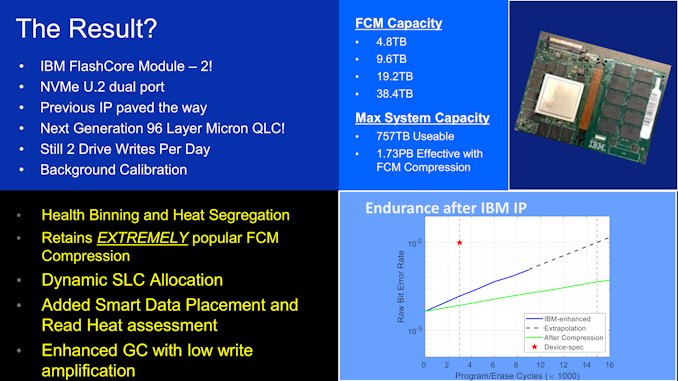
At Flash Memory Summit this week (online for the first time), Western Digital is showing off three new SSD products and have outlined the company’s areas of strategic focus in a keynote presentation.


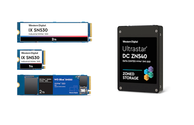
First up, Western Digital is commercializing NVMe Zoned Namespaces (ZNS) technology with the new Ultrastar DC ZN540 datacenter SSD. We covered ZNS in depth earlier this year after the extension to the NVMe standard was ratified. Western Digital has been one of the strongest proponents of ZNS, so it’s no surprise that they’re one of the first to launch a zoned SSD product.


The ZN540 is based on a similar hardware platform to their existing traditional enterprise/datacenter SSDs like the Ultrastar DC SN640 and SN840. The ZN540 is a 2.5″ U.2 SSD using 3D TLC NAND and a Western Digital-designed SSD controller, and offers capacities up to 8TB with dual-port PCIe 3.0 support. The most significant hardware difference is a big decrease in the amount of RAM the SSD needs compared to the usual 1GB per 1TB ratio; Western Digital isn’t ready to disclose exactly how much RAM they are shipping in the ZN540, but it should be a nice decrease in BOM.


The new ZN540 also renders the Ultrastar DC SN340 mostly obsolete. The SN340 was designed to get some of the benefits of a zoned SSD by using a Flash Translation Layer that works with 32kB blocks instead of the usual 4kB. That enables a DRAM reduction by a factor of eight, at the expense of much lower random write performance, especially for small block sizes. ZNS SSDs simply prohibit random writes in the first place rather than silently deliver horrible performance with extremely high write amplification, and the ZNS interface allows software to be properly informed of these limitations and provides tools to cope with them.


The Ultrastar DC ZN540 is currently sampling to major customers. Software support for ZNS SSDs is fairly mature at the OS level in the Linux kernel and related tooling. Application-level support for zoned storage is more of a work in progress, but Western Digital and others have been hard at work. Zoned storage backends already exist for some well-known applications like the Ceph cluster filesystem and RocksDB key-value database.


Next up, Western Digital is introducing their first industrial-grade NVMe SSD. Western Digital’s industrial and automotive lineup currently consists of eMMC and UFS modules and SD/microSD cards. The new Western Digital IX SN530 NVMe SSD is an industrial/automotive grade version of the PC SN530, OEM counterpart to the retail SN550. These are DRAMless NVMe SSDs, albeit some of the best-performing DRAMless SSDs on the market. The IX SN530 will be available with capacities of 256GB to 2TB of TLC NAND, or operating as SLC NAND with capacities of 85-340GB and drastically higher write endurance. One of the main target markets for the IX SN530 will be automotive applications, where the push toward self-driving cars is increasing storage capacity and performance requirements.


The TLC-based variants of the IX SN530 are sampling now, and the SLC versions will start sampling in January.


Western Digital IX SN530 SSD Specifications
Capacity 85 GB 170 GB 340 GB 256 GB 512 GB 1 TB 2 TB
Form Factor M.2 2280 or M.2 2230 M.2 2280
Controller WD in-house
DRAM None
NAND Flash Western Digital 96L SLC Western Digital 96L TLC
Sequential Read 2400 MB/s 2400 MB/s 2500 MB/s
Burst Sequential Write

 
900 MB/s 1750 MB/s 1950 MB/s 900 MB/s 1750 MB/s 1950 MB/s 1800 MB/s
Sustained Sequential Write 900 MB/s 1750 MB/s 1950 MB/s 140 MB/s 280 MB/s 540 MB/s 525 MB/s
Random Read IOPS 160k 310k 410k 160k 310k 410k 370k
Random Write IOPS 180k 330k 350k 85k 150k 350k 300k
Projected Write Endurance 6000 TB 12000 TB 24000 TB 650 TB 1300 TB 2600 TB 5200 TB


Since the IX SN530 will be available in capacities up to 2TB, Western Digital is also adding a 2TB model to the related WD Blue SN550 consumer NVMe SSD, extending their entry-level NVMe product line now that such high capacities are no longer just for high-end SSDs. The new WD Blue SN550 2TB model is already in production and working its way through the supply chain, so it should be available for purchase soon.


WD Blue SN550 SSD Specifications
Capacity 250 GB 500 GB 1 TB 2 TB
Form Factor M.2 2280 PCIe 3.0 x4
Controller WD in-house
DRAM None
NAND Flash Western Digital/SanDisk 96L 3D TLC
Sequential Read 2400 MB/s 2400 MB/s 2400 MB/s 2600 MB/s
Sequential Write 950 MB/s 1750 MB/s 1950 MB/s 1800 MB/s
Random Read 170k IOPS 300k IOPS 410k IOPS 360k IOPS
Random Write 135k IOPS 240k IOPS 405k IOPS 384k IOPS
Warranty 5 years
Write Endurance 150 TB

0.3 DWPD
300 TB

0.3 DWPD
600 TB

0.3 DWPD
900 TB

0.25 DWPD
MSRP $44.99 $53.99 $94.99 $249.99

Several performance metrics for the 2TB SN550 are slower than the 1TB model and the write endurance rating didn’t scale with capacity, so the 2TB WD Blue SN550 isn’t a groundbreaking product. The initial MSRP is quite a bit higher than a DRAMless NVMe SSD should be going for, even accounting for the fact that WD tends to have the best-performing DRAMless SSDs on the market.


Western Digital also used their keynote presentation to give a rundown on various areas the company is focusing on as part of their strategy to be more than just a NAND and drive manufacturer.


And in fact, we didn’t get to hear much at all about their NAND flash memory itself, despite the name of the conference. Western Digital and Kioxia announced their 112-layer fifth-generation BiCS 3D NAND in January 2020, but the new WD drives announced today are still using 96-layer TLC. We did catch a few potential references to future generations of 3D NAND: they have above 100 layers in production now and will reach 200 layers “pretty soon”, they’ll be moving the peripheral circuits to be above and below the memory rather than alongside (following in the footsteps of Micron, Intel and Hynix), 2Tbit dies will be coming at some point, and I/O speeds going from 400MT/s to 2GT/s over four generations. Since those were all passing mentions, we’re hesitant to take any of it as a solid indication of what to expect from their sixth generation 3D NAND, and we certainly don’t have any indication of when that will be going into production or hitting the market.


Aside from the Zoned Storage work we’ve already covered, Western Digital mentioned several areas of ongoing development. They are a big proponent of the RISC-V CPU architecture and have open-sourced some RISC-V core designs already, but we don’t have a clear picture of what—if any—Western Digital products have already started using RISC-V CPU cores. NVMe over Fabrics is one of the most important datacenter storage technologies, and Western Digital is participating through their OpenFlex storage systems and the RapidFlex NVMeoF controller technology they acquired last as from Kazan Networks.


Western Digital is talking about computational storage, but only in the broadest terms—reiterating all the tantalizing possibilities, but not yet announcing any specific hardware development plans. In the area of security, Western Digital highlighted their membership in the OpenTitan project for developing open-source hardware root of trust technology. This is driven by the industry consensus that features like Secure Boot aren’t just useful for protecting the boot process of your operating system, but for verifying all the intelligent components in a system that handle sensitive data.


Source: AnandTech – Western Digital at FMS 2020: Zoned SSDs, Automotive NVMe And More

Microchip Announces PCIe 5.0 And CXL Retimers

Microchip is entering the market for PCIe retimer chips with a pair of new retimers supporting PCIe 5.0’s 32GT/s link speed. The new XpressConnect RTM-C 8xG5 and 16xG5 chips extend the reach of PCIe signals while adding less than 10ns of latency.


As PCIe speeds have increased, the practical range of PCIe signals across a circuit board has decreased, requiring servers to start including PCIe signal repeaters. For PCIe gen3, mostly-analog redriver chips were often sufficient to amplify signals. With PCIe gen4 and especially gen5, the repeaters have to be retimers that operate in the digital domain, recovering the clock and data from the input signal with awareness of the PCIe protocol to re-transmit a clean copy of the original signal. Without retimers, PCIe gen5 signals only have a range of a few inches unless expensive low-loss PCB materials are used, so large rackmount servers with PCIe risers at the back and drive bays in the front are likely to need retimers in several places.


Microchip’s new XpressConnect retimers add less than 10ns of latency, considerably better than the PCIe requirements of around 50–60ns. This also helps make the new XpressConnect retimers suitable for use with CXL 1.1 and 2.0, which use the same physical layer signaling as PCIe gen5 but target more latency-sensitive use cases. These retimers are the first Microchip products to support PCIe 5.0, but the rest of their PCIe product lineup including PCIe switches and NVMe SSD controllers will also be migrating to PCIe gen5.


The XpressConnect retimers come in 8-lane and 16-lane variants, both supporting bifurcation to smaller link widths, so that a single retimer can be used for multiple x1, x2 or x4 links. The retimers conform to Intel’s specification for the BGA footprint and pinouts of PCIe retimers (13.4×8.5mm for 8 lanes, 22.8×8.9mm for 16 lanes), so these chips will eventually be competing against alternatives that could be used as drop-in replacements.


Common uses for PCIe retimers will be on drive bay backplanes, riser cards, and on large motherboards to extend PCIe 5.0 to the slots furthest from the CPU. Retimer chips will not necessarily be needed for every PCIe or CXL link in a server, but they are going to be an increasingly vital component of the PCIe ecosystem going forward. PCIe/CXL connections with a short distance from the CPU to the peripheral and few connectors will usually not need retimers, and riser or adapter cards that use PCIe switches to fan out PCIe connectivity to a larger number of lanes will already be re-transmitting signals and thus don’t need extra retimers.


Microchip’s XpressConnect PCIe 5.0 / CXL 2.0 retimers are currently sampling to customers, and are being incorporated into an Intel reference design for PCIe riser boards. Mass production will begin in 2021.


Source: AnandTech – Microchip Announces PCIe 5.0 And CXL Retimers

Intel Xe Graphics: An Interview with VP Lisa Pearce

Bringing a new range of hardware to market is not an easy task, even for Intel. The company has an install base of its ‘Gen’ graphics in hundreds of millions of devices around the world, however the range of use is limited, and it doesn’t tackle every market. This is why Intel started to create its ‘Xe’ graphics portfolio. The new graphics design isn’t just a single microarchitecture – by mixing and matching units where needed, Intel has identified four configurations that target key markets in its sights, ranging from the TeraFLOPs needed at the low-end up to Peta-OPs for high performance computing.


Leading up the charge on the driver and software side of the equation is Intel’s Lisa Pearce. Lisa is a 23 year veteran of Intel, consistently involved in Intel’s driver application and optimization, collaboration with independent software vendors, and Lisa now stands as the Director and VP of Intel’s Architecture, Graphics and Software Group, and Director of Visual Technologies. Everything under that bucket of Intel’s Graphics strategy as it pertains to drivers and software, all the way from integrated graphics through gaming and enterprise into high-performance, is in Lisa’s control.


Source: AnandTech – Intel Xe Graphics: An Interview with VP Lisa Pearce