Corsair Launches MP600 CORE and MP600 PRO PCIe 4.0 SSDs

Corsair is launching a new round of PCIe 4.0 M.2 NVMe SSDs based on the latest reference designs from Phison plus Corsair’s own heatsink designs. Starting off, the Corsair MP600 CORE is their first PCIe 4.0 SSD with QLC NAND flash memory. This uses the older Phison E16 controller so peak performance only pushes a little bit beyond what would be possible with PCIe 3.0, but it’s still a step up from the Corsair MP400.


Corsair MP600 CORE Specifications
Capacity 1 TB 2 TB 4 TB
Form Factor M.2 2280 PCIe 3 x4
Controller Phison E16
NAND Flash 3D QLC
DRAM 1 GB 2 GB
Sequential Read (MB/s) 4700 4950
Sequential Write (MB/s) 1950 3700 3950
Random Read IOPS (4kB) 200k 380k 630k
Random Write IOPS (4kB) 480k 580k
Power Consumption Read 5.6 W 6.3 W 6.0 W
Write 5.7 W 6.8 W 7.4 W
Warranty 5 years
Write Endurance 200 TB

0.1 DWPD
400 TB

0.1 DWPD
800 TB

0.1 DWPD
MSRP $154.99

(15¢/GB)
$309.99

(15¢/GB)
$644.99

(16¢/GB)


We have a sample of the 2TB MP600 CORE in hand, waiting for its turn to run through our new SSD test suite.


Next is Corsair’s new top of the line SSD, the MP600 PRO based on the Phison E18 controller and TLC NAND flash memory. The MP600 PRO takes over the top spot from the original MP600, Corsair’s Phison E16 + TLC product that launched in 2019 alongside the first AMD Ryzen CPUs to support PCIe 4.0. The new MP600 PRO will be available with either the standard aluminum heatsink, or with a water block in a variant sold as the MP600 PRO Hydro X.


We don’t have full specs for the MP600 PRO yet, but performance should be basically the same as other Phison E18 drives using 96L TLC, meaning peak sequential transfer rates around 7 GB/s for both reads and writes. The MP600 PRO will be available with capacities up to 2TB. Since Corsair isn’t ready with review samples of the MP600 PRO quite yet, we expect retail availability will be a bit later than for the MP600 CORE.


Source: AnandTech – Corsair Launches MP600 CORE and MP600 PRO PCIe 4.0 SSDs

AMD Reports Q4 2020 Earnings: Analyst Q&A Transcript

At the end of every financial call, invited financial analysts have an opportunity to probe the key members of the company on the numbers, as well as future products. We just had AMD’s Q4 2020 Financial call, covering all of Q4 developments as well as 2020 as a whole. On the call was CEO Dr. Lisa Su and CFO Davinder Kumar.


Source: AnandTech – AMD Reports Q4 2020 Earnings: Analyst Q&A Transcript

AMD Reports Q4/FY 2020 Earnings: Record Revenues Repeat

Needing no introduction, AMD this afternoon is the second of the PC chip titans to announce their earnings for the quarter and for the full 2020 calendar year. The company has continued to ride high on the success of its Zen architecture-based CPUs and APUs, as well as the recent launch of the Playstation 5 and Xbox Series X|S. As a result, these products have propelled AMD to another record quarter and another record year, as the company continues to hit revenue records while recording an increasingly tidy profit in the process.


For the fourth quarter of 2020, AMD reported $3.24B in revenue, a 53% jump over the same quarter a year ago. As a result, Q4’2020 was (once again) AMD’s best quarter ever, built on the back of strong sales across virtually the entire company. And AMD’s gross margin has held steady at 45%, the same as Q4’19.


Meanwhile, in what was already a strong quarter for the company, AMD also realized some one-off gains related to an income tax valuation allowance, which added another $1.3B to AMD’s net income. As a result, the company booked a massive profit of $1.78B for the quarter alone. Otherwise, excluding that one-off gain and looking at AMD’s non-GAAP results, the company still booked 66% more in net income in Q4’20 than they did the year-ago quarter. So not only is AMD pulling in record revenues for the quarter, but that is translating into much higher profits as well.


AMD Q4 2020 Financial Results (GAAP)
  Q4’2020 Q4’2019 Q3’2020 Y/Y Q/Q
Revenue $3.2B $2.1B $2.8B +53% +16%
Gross Margin 45% 45% 44% Flat +1pp
Operating Income $570M $348M $449M +64% +27%
Net Income $1781M* $170M $390M +948% +357%
Earnings Per Share $1.45 $0.15 $0.32 +867% +353%


As for AMD’s full-year earnings, the company has been having strong quarters all year now, so unsurprisingly this is reflected in their full-year results. Overall, for 2020 AMD booked $9.76B in revenue, which was an increase of 45% over 2019, and once again a record for the company. Amusingly, AMD’s gross margin for the entire year was also 45%, which is one percentage point higher than 2019’s.


Like AMD’s quarterly results, their full-year results are also distorted a bit by their one-off tax benefit. By GAAP standards AMD booked an incredible $2.49B in net income for 2020. However removing that tax benefit brings their net income down to around $1.4B – or a non-GAAP $1.56B – which is still a huge year-over-year increase in profitability for the company, more than doubling their 2019 non-GAAP performance. Despite AMD’s gross margin only improving by a single point, AMD is increasingly enjoying the benefits of scale, with record-breaking product shipments turning into profits for the company.


AMD FY 2020 Financial Results (GAAP)
  FY 2020 FY 2019 FY 2018 Y/Y
Revenue $9.8B $6.7B $6.5B +45%
Gross Margin 45% 43% 38% +2pp
Operating Income $1369M $631M $451M +117%
Net Income $2490M* $341M $337M +630%
Earnings Per Share $2.06 $0.30 $0.32 +587%


Moving on to individual reporting segments, 2020 marks an interesting year for AMD given the company’s unusual split into two major segments. Normally AMD’s Compute and Graphics segment is by far and away the flag bearer for the company’s earnings, but the launch of the latest generation of consoles, combined with ever-improving EPYC sales, means that the Enterprise, Embedded and Semi-Custom segment also saw a very strong quarter.


For Q4’20, AMD’s Computing and Graphics segment booked $1.96B in revenue, an 18% improvement over the year-ago quarter. According to the company, the biggest contributor to the increase here is strong sales of Ryzen processors. AMD does not break down the numbers by chip sales volumes, but Ryzen chip average selling prices (ASPs) themselves were actually down year-over-year, which AMD attributes to increased (and record) Ryzen mobile sales. The recent release of AMD’s Ryzen 5000 desktop CPUs did bring up ASPs on a quarterly basis, but Ryzen 5000 CPUs as a small piece of a larger whole, especially as they remain in short supply.


As for AMD’s GPU operations, the company reports that Radeon ASPs increased year-over-year and quarter-over-quarter, thanks to the recent launch of the Radeon RX 6000 series. Perhaps tellingly, the company is not offering any volume comparisons on a year-over-year basis, a likely indicator that AMD’s GPU sales are getting throttled by their supply constraints, especially as the company continues to ramp up the RX 6000 family.


AMD Q4 2020 Reporting Segments
  Q4’2020 Q4’2019 Q3’2020

Computing and Graphics

Revenue $1960M $1662M $1667M
Operating Income $420M $360M $384M

Enterprise, Embedded and Semi-Custom

Revenue $1284M $465M $1134M
Operating Income $243M $45M $141M


Meanwhile, AMD’s Enterprise, Embedded and Semi-Custom segment booked $1.28B in revenue for the quarter. The 176% year-over-year increase in revenue was driven by a mix of both improved EPYC sales, and of course the launch of the latest-generation gaming consoles. Unfortunately AMD doesn’t break down how much each of these product groups contributed, so it’s hard to say how much of this growth is the EPYC side of matters as opposed to the more irregular game console revenue. At any rate, according to AMD Q4 of 2020 was another record quarter on the server side of matters, with AMD recording record server revenue thanks to continued cloud and enterprise sales growth.


Looking forward, AMD is expecting a very promising first quarter of 2021 and beyond, albeit with expectations tempered by ongoing supply shortages. At this point the company has little trouble selling everything it can make, especially with the continued high demand for tech products spurred on by the pandemic. So a lot of what’s driving AMD’s future, especially over the next quarter or two, is based on just how many 7nm wafers the company can get out of TSMC. For that reason, AMD’s 2021 revenue forecast is relatively conservative for a growing AMD, as the company is projecting a 37% increase in non-GAAP revenue.


On the product side of matters, AMD will be enjoying a largely new and refreshed slate of product lines. The company’s Zen 3 architecture has begun shipping in laptops in the form of the new Cezanne APU, and the EPYC Milan family of server CPUs is set to launch later in the quarter. On top of that, they have ongoing sales of their Ryzen 5000 desktop CPUs, as well as the continued ramp-up and further releases of Radeon RX 6000 (RDNA2) GPUs, with new desktop and mobile parts expected in the first half of this year. Consequently, AMD is expecting a good year across all of its product lines, with all of its product lines expecting to see further growth.


Source: AnandTech – AMD Reports Q4/FY 2020 Earnings: Record Revenues Repeat

NVIDIA Launches Server Certification Program, Offering Direct Technical Support

While a good deal of NVIDIA’s success in servers over the last decade has of course come from their proficient GPUs, as a business NVIDIA these days is much more than a fabless GPU designer. With more software engineers than hardware engineers on staff, it’s software and ecosystem plays that have really cemented NVIDIA’s position as the top GPU manufacturer, and created a larger market for their GPUs. At the same time, it’s these ecosystem plays that have allowed NVIDIA to build a profit-printing machine, diversifying beyond just GPU sales and moving into systems, software, support, and other avenues.


To that end, NVIDIA this morning is formally rolling out a new ecosystem play aimed at high-end deep learning servers, which the company is branding as NVIDIA-Certified Systems. Soft-launched back in the fall, today the company is giving the program a more proper introduction, detailing the program and announcing some of the partners. Under NVIDIA’s plan, going forward customers can opt to buy NVIDIA-Certified systems if they want an extra guarantee on system performance and reliability, as well as opt in to buying support contracts to get access to direct, full-stack technical support from NVIDIA.


Conceptually, the certification program is rather straightforward, due in large part to its hardware requirements. Systems first need to be using NVIDIA’s A100 accelerators, along with Mellanox Ethernet adapters and DPUs. Or in other words, the servers already need to be using NVIDIA silicon where available. OEMs can then submit systems meeting these hardware requirements to NVIDIA, who will test the systems across multiple metrics, including multi-GPU and multi-node DL performance, network performance, storage performance, and security (secure boot/root of trust). Systems that pass these tests can then be labeled as NVIDIA-Certified.


Those certified systems, in turn, are eligible for additional full-stack technical support through NVIDIA and the OEM. Customers can opt to buy multi-year support contracts, which entitles them to support through the OEM and NVIDIA. NVIDIA essentially assumes responsibility for all software support above the OS, including their hardware drivers, CUDA, their wide collection of frameworks and libraries, and even major open source libraries like TensorFlow. The latter is what makes NVIDIA’s support proposition particularly valuable, as they’re essentially committing to helping customers with any kind of GPU or deep learning-related software issue.


Of course, that support won’t come for free: this is where NVIDIA will be making their money. While NVIDIA is not charging OEMs for certification (so there’s no additional certification tax baked into the hardware), support contracts are priced based on the number of GPUs. In one example, NVIDIA has stated that a 3 year support contract for a dual-A100 system would be $4,299, or about $715 per-year per-GPU for support. So one can imagine how quickly this ratchets up for larger 4 and 8 way A100 systems, and then again for multiple nodes.


For NVIDIA and its OEM partners, the creation of a certification program is a straightforward way to try to further grow the market for deep learning servers, especially for mid-sized businesses. The market for AI hardware has been booming, and NVIDIA wants to keep it that way by making it easier for potential customers to use their wares. NVIDIA already has the top-end of the market covered in this respect with their direct relationships with the hyperscalers – and by extension their small-cap cloud computing customers – so a hardware certification program fills the middle tier for organizations that are going to run their own servers, but aren’t going to be a massive customer that gets personalized attention.


As for those customers, NVIDIA’s server certification and support programs are designed to eliminate (or at least mitigate) the risks of making significant investments into NVIDIA hardware. That means being able to buy a system where the vendor (in this case the duo of NVIDIA and the OEM) can vouch for the performance of the system, as well as guarantee it will be able to properly run various AI packages, such as NVIDIA’s NGC catalog of GPU-optimized and containerized software.


Altogether, NVIDIA is launching with 14 certified systems, with the promise of more certified systems to come. For the first wave of systems, participating OEMs include Dell, Gigabyte, HPE, Inspur, and Supermicro, all of whom are frequently participants in new NVIDIA server initiatives.


With all that said, NVIDIA’s server certification program is unlikely to significantly change how things work for most of the company’s customers; but it’s a program that seems primed to address a specific niche for NVIDIA and its OEM partners. For companies that are interested in GPU computing but are looking for a greater degree of support and certainty, this would address those needs. Which, to bring things full circle, it’s exactly by addressing those sorts of needs with ecosystem plays like server certification that NVIDIA has been so successful in the server GPU market over the last decade.


Source: NVIDIA


Source: AnandTech – NVIDIA Launches Server Certification Program, Offering Direct Technical Support

Intel Teases Ponte Vecchio Xe-HPC Power On, Posts Photo of Server Chip

In what’s turning into an Xe sort of day, Intel’s GPU guru and frontman for their GPU division, Raja Koduri, has tweeted that the company is getting ready to begin power on testing for their forthcoming high-end server GPU, the Xe-HPC based Ponte Vecchio. And along with this announcement, Koduri has also posted a somewhat redacted photo of the sizable chip.


According to Koduri, Ponte Vecchio incorporates “7 advanced silicon technologies,” likely referring to everything from the four different process nodes used to make the chiplets, to memory stacks, and including the Foveros packaging.


Ponte Vecchio is a keystone project for Intel’s GPU division. Along with being the largest and grandest of their Xe GPUs, the chip will be at the heart of the Aurora supercomputer, Intel’s most recent supercomputer win. So a lot is riding on the chip, and no doubt Intel’s engineers are eager to see a successful power-on test.


Source: AnandTech – Intel Teases Ponte Vecchio Xe-HPC Power On, Posts Photo of Server Chip

Sony Launches Xperia PRO 5G … for $2499

Last year in February Sony had launched the Xperia 1 II, as well as teasing a sibling device called the Xperia PRO. This latter variant of the phone was meant to be a professional variant of the Xperia 1 II, in a more rugged form-factor, as well as integrating a HDMI input port.


Today, almost a whole year later, Sony is ready to finally to launch the Xperia PRO 5G, with availability starting today at a staggering price tag of $2499.


The peculiarity about the Xperia PRO 5G are two key features: a HDMI input port alongside the usual USB-C port, as well as additional mmWave 5G connectivity in the form of four antennas, more than the usual two or three we find in other consumer models.


Sony is trying to position the Xperia PRO as a professional accessory for broadcast video, where the phone directly attaches to your camera feed via HDMI and is able to directly upload to the internet. It’s a very niche use-case, however Sony is trying to replace several discrete devices in one: The Xperia PRO can serve simultaneously as a high-quality monitor, and actually outperform most other dedicated camera monitors out there thanks to its 6.5” 3840 x 1644 HDR OLED screen, as well as serving as a cellular video streamer, a kind of device that usually alone goes for $1000 to $1500.


Furthermore, Sony is doing a lot of fanfare about the phone’s 4 mmWave antennas and how it’ll be able to achieve much better, stable, and uniform reception compared to other devices in the market which employ only 2 or 3 antennas. The caveat here is of course that this will only ever get used when under actual mmWave coverage, which is still a very limited number of locations in the US. Of course, the phone will fall back to sub-6GHz 5G and LTE whenever there’s no mmWave coverage.


So, while the $2499 price tag might sound absolutely outrageous at first, it’s not much more expensive than other discrete solutions such as a dedicated monitor as well as competing, feature poorer cellular streaming devices. Where I do think Sony dropped the ball here is in terms of software features: the Xperia PRO lacks more commonly found features in dedicated monitors such as wave forms or vector scopes, and also lacks any kind of camera control or status features, even with Sony’s own line-up of cameras. For the device being now launched almost a whole year after its initial announcement, that’s extremely disappointing. During the Q&A briefing, it seems that Sony is aware of these features missing, but offered no concrete answers on whether they’ll continue to evolve the product from a software standpoint.


The Xperia PRO is otherwise feature identical to an Xperia 1 II – including the Snapdragon 865 SoC, the triple-camera setup, screen, and battery size, though DRAM and storage are upped to 12GB and 512GB. Furthermore, Sony says that the Xperia PRO is only launching in the US for $2499, with no current plans for availability in other markets.


Related Reading:


Source: AnandTech – Sony Launches Xperia PRO 5G … for 99

AMD's Ryzen 5000 Lucienne: Not Simply Rebranded Ryzen 4000 Renoir

AMD came in for some harsh criticism when it announced that its new Ryzen 5000 Mobile U-series processors would not all be using its latest core design. At the product announcement, we were told that some of the U-series processors would be based on the previous Zen 2 generation, and this was mainly for partners to take advantage of the new naming scheme but also reuse designs with the same ballpark performance. A number of tech enthusiasts (including myself, I have to say) scoffed at this as it made the whole system complex. It’s still complex, but we’ve come to understand that these latest Zen 2 based mobile processors also include a whole raft of updates that make them a better version of what they are.


To simplify things I’m going to call these products by their AMD codenames. The older Zen 2 processors are called Renoir, and the newer Zen 2 processors are called Lucienne. Here is a list of the new Ryzen 5000 U-Series, with Lucienne listed in yellow.


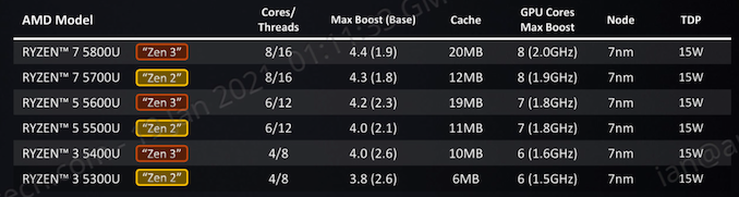
Renoir, for all intents and purposes, was a very successful product for AMD. Placed in the Ryzen 4000 Mobile series, it became the bedrock of AMD’s mobile portfolio and has been installed in around 100 design wins since it came to market. Lucienne on the other hand is a minor player in the latest Ryzen 5000 Mobile series. It doesn’t have the updates that the new Zen 3 cores have, but we have since learned that on the power side of things, rather than being a copy of Renoir, it is almost certainly Renoir Plus.


What Lucienne brings to the table over Renoir comes in discrete categories.


Memory Controller


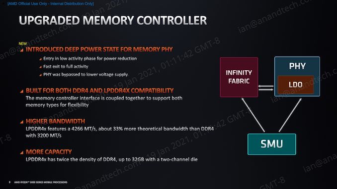
The memory controller in Lucienne is now able to decouple its voltage from the cores and enter a lower power state when not in use or for low bandwidth reasons. This ultimately saves power, and AMD has enabled it to bypass particular voltage indicators to help it stay in the low voltage state. Aside from the cores and the graphics, the other two consumers of power inside a mobile processor is the internal communications and the external communications, of which the memory controller falls under the latter. AMD has also put into place a system by which the memory controller can wake to a full bandwidth state faster than before, enabling better responsivity from those deep sleep states.


On top of this, the memory controller can now support double the capacity of memory from Renoir: up to 64 GB of DDR4-3200, or up to 32 GB of LPDDR4X-4267. Using DDR4 means the system can have more peak memory, as well as being user adjustable, however LPDDR4X trades those in for faster bandwidth overall (68.4 GB/s vs 51.2 GB/s).


Per-Core Voltage Control


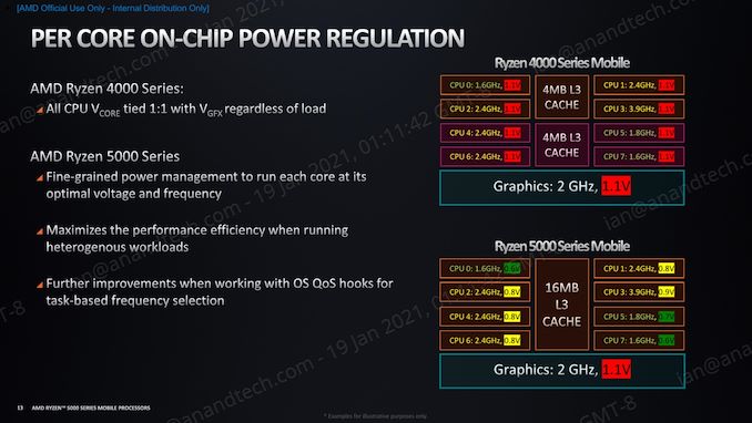
In similar circumstances to the memory controller, having voltage control of each individual core in a mobile processor is one angle to both maximize performance when needed and minimize power loss when idle. In Renoir, all of the cores can adjust their frequency, but they all had to run at the same voltage. Lucienne changes that such that each core can adjust its voltage independently, enabling a finer grained power management and a more optimal power-efficient system. There are also additional hooks that operating systems can use if it knows high performance cores are needed in advance.


Preferred Core


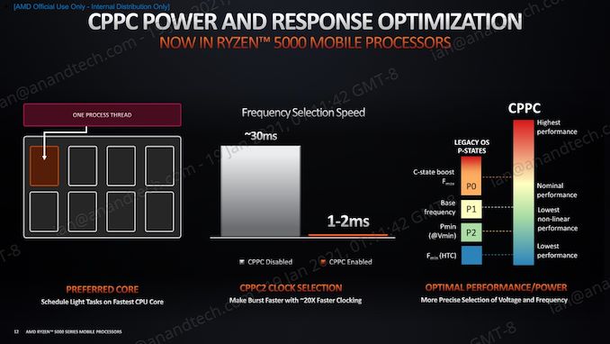
When we speak about turbo, historically it has been assumed that any core can reach the highest single core turbo frequency, and that the workload is sometimes shifted between cores to help with thermal management. When a system uses a preferred core however, it means that a system could be optimized for that specific core, and more performance extracted. AMD introduced its Preferred Core technology on the desktop two generations ago, and now it comes to the mobile processors. One core out of the eight on Lucienne silicon will be designated the best core, and through an OS driver (default in Windows) all workloads will be placed on that core preferentially.


Frequency Ramp


One of the features that tie all of this together is how quickly a core can move from idle to peak performance and back again. If a system takes too long to ramp up to speed, or ramp back down, then responsiveness and power is lost. A typical modern system is expected to ramp up from idle to peak frequency within two frames at 60 Hz, or 32 milliseconds, however the latest systems from AMD and Intel have done it much faster, often within 16 ms. AMD’s enhanced clock gating technology is now enabling Lucienne to reduce that down to 1-2 milliseconds. This means that a system could easily ramp up and down between each keystroke on a keyboard, supplying immediate responsiveness to a user while keeping the total power use down. In the 16-32 millisecond regime, typing on a keyboard may have meant a core being active almost continuously, however making this change faster affords a lot of power savings through these transitions.


Continuous Performance Levels


The legacy way for an operating system to command performance is through performance states, or P-states. In this instance the OS would request a specific level of power and performance from the processor based on its detected workload, and the processor would respond. This was originally implemented during a time when turbo was first coming to modern processors, and workload analysis was better done through the operating system. Now we can do this level of monitoring on the processor directly, and through an OS driver (already part of Windows), with system support that level of frequency control can be passed back down to the processor. The processor also gets an effective continuous distribution of performance, rather than discrete P-states.


While Renoir had P-states, Lucienne gets the benefit of CPU-level performance requests.


Faster Integrated Graphics


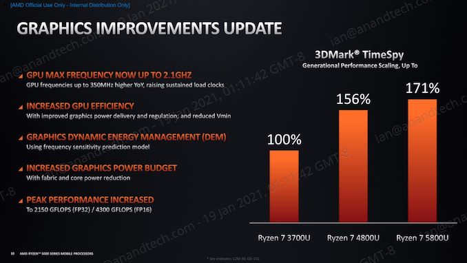
With the additional power control elsewhere on the core, how the power delivery works to the integrated graphics was also adjusted to allow for better regulation and ultimately a lower minimum voltage. Through firmware AMD has enabled a frequency sensitive prediction model that allows the GPU to adjust its voltage and frequency based on its dynamic energy management. Coupled with the better regulation and the power budget balancing done between CPU, interconnect, DRAM, and the GPU, more power budget is available for the GPU. For Lucienne, this means +150 MHz on the peak IGP speeds compared to Renoir.


Slide shows Cezanne numbers, but applies to Lucienne as well


But I thought Lucienne Silicon was the same as Renoir Silicon?


This is the big question. We asked AMD if Lucienne was the same stepping of Renoir, and the answer was not exactly committal in one direction or the other. The simple answer is yes, however AMD wants to make clear that substantial changes were made to firmware and manufacturing that means that despite the transistor layout being identical, there are features of Lucienne that would never have worked in Renoir without the changes that have been made.


So while yes it is the same silicon layout and floorplan, some of these features weren’t possible in Renoir. AMD built in these features perhaps knowing that they couldn’t be enabled in Renoir, but sufficient changes and improvements at the manufacturing stage and firmware stage were made such that these features were enabled in Lucienne. More often than not these ideas often have very strict time windows to implement, and even if they are designed in the hardware, there is a strict cut-off point by which time if it doesn’t work as intended, it doesn’t get enabled. Obviously the best result is to have everything work on time, but building CPUs is harder than we realize.


Sometimes I wonder how we ever get these rocks powered by lightning to work in the first place.


Source: AnandTech – AMD’s Ryzen 5000 Lucienne: Not Simply Rebranded Ryzen 4000 Renoir

Intel Iris Xe Video Cards Now Shipping To OEMs: DG1 Lands In Desktops

Following plans first unveiled last year during the launch of their DG1 GPU, Intel sends word this morning that the first Iris Xe video cards have finally begun shipping to OEMs. Based on the DG1 discrete GPU that’s already being used in Intel’s Iris Xe MAX laptop accelerators, the Iris Xe family of video cards are their desktop counterpart, implementing the GPU on a traditional video card. Overall, with specifications almost identical to Xe MAX, Intel is similarly positioning these cards for the entry-level market, where they are being released as an OEM-only part.


As a quick refresher, the DG1 GPU is based on the same Xe-LP graphics architecture as Tiger Lake’s integrated GPU. In fact, in broad terms the DG1 can be thought of as a nearly 1-to-1 discrete version of that iGPU, containing the same 96 EUs and 128-bit LPDDR4X memory interface as Tiger Lake itself. Consequently, while DG1 is a big first step for Intel – marking the launch of their first discrete GPU of the modern era – the company is planning very modestly for this generation of parts.


Intel Desktop GPU Specification Comparison
  Iris Xe

dGPU
Tiger Lake

iGPU
Ice Lake

iGPU
Kaby Lake

iGPU
ALUs 640

(80 EUs)
768

(96 EUs)
512

(64 EUs)
192

(24 EUs)
Texture Units 40 48 32 12
ROPs 24? 24 16 8
Peak Clock 1650MHz? 1350MHz 1100MHz 1150MHz
Throughput (FP32) 2.11 TFLOPs 2.1 TFLOPs 1.13 TFLOPs 0.44 TFLOPs
Geometry Rate

(Prim/Clock)
2 2 1 1
Memory Clock LPDDR4X-4266? LPDDR4X-4266 LPDDR4X-3733 DDR4-2133
Memory Bus Width 128-bit 128-bit

(IMC)
128-bit

(IMC)
128-bit

(IMC)
VRAM 4GB Shared Shared Shared
TDP ~25W? Shared Shared Shared
Manufacturing Process Intel 10nm SuperFin Intel 10nm SuperFin Intel 10nm Intel 14nm+
Architecture Xe-LP Xe-LP Gen11 Gen9.5
GPU DG1 Tiger Lake

Integrated
Ice Lake Integrated Kaby Lake Integrated
Launch Date 01/2021 09/2020 09/2019 01//2017


The first DG1 GPUs were shipped in the fall as part of Intel’s Iris Xe MAX graphics solution for laptops. At the time, Intel also indicated that a desktop card for OEMs would also be coming in 2021, and now, right on schedule, those desktop cards have begun shipping out.


Overall, Intel is taking a very OEM-centric approach to their DG1 products, and that goes for both laptops and the desktops. Even the desktop Iris Xe cards won’t be sold as retail – as entry-level cards, they are unlikely to fly off of shelves – and instead are only being sold to OEMs for use in pre-built systems. And even then, the cards were co-designed with ecosystem partners – of particular note, ASUS – rather than Intel building and shipping out their own video cards. So by desktop video card standards, Intel is being somewhat hands-off at the moment.


In a curious twist, the desktop cards will have slightly lower specifications than the laptop parts. While I’m still waiting to hear what the TDPs and final clockspeeds will be, Intel’s announcement confirms that the Iris Xe cards will only ship with 80 of 96 EUs enabled, rather than being fully-enabled in the case of the laptop parts. Given that this is an entry-level part, any further drop in performance isn’t doing the part any favors, but at the same time it was never going to be a speed-demon to begin with. At any rate, given that no chip has perfect yields, we now know where salvaged DG1 chips are going.


Meanwhile, like their laptop counterparts, the Iris Xe desktop cards will ship with 4GB of LPDDR4X memory. Intel has also confirmed that the cards will ship with up to three display outputs, with ASUS’s card using a mix of HDMI, DisplayPort, and even a DL-DVI-D port.


Colorful’s DG1 Card


As for Intel’s target market, the company is targeting what they’re calling the “high-volume, value-desktop market.” Notably, unlike the Iris Xe MAX launch, Intel’s (admittedly brief) news release doesn’t spend much time focusing on the cards as a secondary accelerator, and instead are promoting these as a superior solution over existing graphics options. Given the focus on things like AV1 decoding, HDR support, and deep learning inference performance, I’m assuming that these will primarily be showing up in Atom (Gemini Lake Refresh) systems. Though it may also show up in low-end Comet Lake Celeron and Pentium systems, where vendors are looking to add a few more display ports and take advantage of the additional hardware accelerator blocks for things like video encoding, similar to how Intel positioned Iris Xe MAX for laptops.


Finally, given the OEM-centric nature of today’s launch, Intel isn’t publishing any specific availability dates for their Iris Xe video cards. But we expect that they’ll begin showing up in short order.


Source: AnandTech – Intel Iris Xe Video Cards Now Shipping To OEMs: DG1 Lands In Desktops

AMD Ryzen 9 5980HS Cezanne Review: Ryzen 5000 Mobile Tested

Since AMD’s introduction of its newest Zen 3 core for desktop users, the implementation for notebooks and mobile users has been eagerly awaited. In a single generation, on the same manufacturing process, AMD extracted +19% more performance per clock (we verified), so for any system that is power limited, extra performance is often very well received. AMD announced its new Ryzen 5000 Mobile processor family at the start of the year, with processors from 15W to 45W+ in the pipeline, and the first mobile systems coming to market in February. AMD sent us a peak example of Ryzen 5000 Mobile for today’s review, the 35W Ryzen 9 5980HS, as contained in the ASUS ROG Flow X13.


Source: AnandTech – AMD Ryzen 9 5980HS Cezanne Review: Ryzen 5000 Mobile Tested

The ASUS ROG Strix X570-E Gaming Motherboard Review

AMD’s AM4 socket has been consistent throughout the entirety of its Ryzen processor’s lifespan, and the latest Zen 3 processors are best suited for the X570 range of motherboards. Today it’s time to see what the mid-range ASUS ROG Strix X570-E Gaming has to offer. Some of its main features include Intel 2.5 GbE and Wi-Fi 6, with dual PCIe 4.0 x4 M.2, with plenty of USB 3.2 G2 connectivity. The ROG Strix X570-E Gaming looks strong and we examine it to see how it stacks up.


Source: AnandTech – The ASUS ROG Strix X570-E Gaming Motherboard Review

ASUS Pro WS WRX80E-SAGE SE WIFI Announced: A Motherboard for AMD Threadripper Pro

In the world of crazy motherboard names, I think ASUS might have won with this one. The new ASUS Pro WS WRX80E-SAGE SE WIFI is a motherboard built for AMD’s upcoming Threadripper Pro processors featuring enough added clout to make the most of 128 lanes of PCIe 4.0.


The extended-ATX (E-ATX) motherboard uses a transposed LGA4094 socket, capable of supporting the 64-core Threadripper Pro 3995WX at 280 W. The socket uses a 16 power stage VRM design with a massive finned heatsink designed to full air from the front of the motherboard to the back in line with the socket and the memory slots, ending in the rear panel which has its own air baffle. There are eight memory slots, enabling 512 GB or 1 TB of DDR4-3200.


The power delivery heatsink seems to be connected to the active chipset heatsink, which in turn has additional heatsinks for all three of the board’s PCIe 4.0 x4 M.2 slots. Other storage options include two U.2 ports, eight SATA ports, and a bundled Hyper M.2 card capable of supporting another four M.2 PCIe 4.0 x4 storage drives.


The board has seven full length supported PCIe 4.0 x16 slots for add-in cards, with these systems aimed at renderers and computational work that can add in additional compute cards. Additional controllers include an Intel X550-AT2 for dual 10 gigabit Ethernet, a baseband management controller (ASUS doesn’t say which one), and Wi-Fi 6 connectivity, likely enabled through Intel’s AX201 or AX210.


Port wise there are nine USB 3.2 Gen 2 ports each with 10 Gbps, and a single USB 3.2 Gen 2×2 Type-C port capable of 20 Gbps. For the front panel, there are two USB 3.2 Gen 2 connectors, as well as USB 3.2 Gen 1 and USB 2.0. Also on the board is BIOS flashback, CMOS reset, what looks like a Realtek ALC1220 audio codec, a COM header, and a wide array of 5-pin fan headers. ASUS’ custom TPU chipset is also onboard.


Users should also be aware that this board appears to take three 12V CPU power connectors, whereas most power supplies only take two. There are also two additional 6-pin PCIe connectors to provide power to the PCIe slots. The rear of the board contains a backplate to assist with board rigidity.


The ASUS Pro WS WRX80E-SAGE SE Wi-Fi is expected to be available in North America from March. Price is as-yet unknown.


Related Reading:


Source: AnandTech – ASUS Pro WS WRX80E-SAGE SE WIFI Announced: A Motherboard for AMD Threadripper Pro

The Google Pixel 5: A Mini-Review – Small Package, Small Value?

The Pixel 5 is a change of tactic for Google, with the company opting to go the route of a lower-cost “premium” or high mid-range component configuration, rather than setting up the Pixel 5 as an all-out flagship phone. Given the company’s product release cadence over the years, always releasing new phones towards the end of the year, just around the corner of the spring next-gen releases. This schedule had always been a disadvantage for Pixel flagships, so maybe Google’s change of strategy here to go for the mid-range is a more sensible approach.


Source: AnandTech – The Google Pixel 5: A Mini-Review – Small Package, Small Value?

Intel Reports Q4 2020 Earnings: 2020 Delivers A Profitable Pandemic

Earnings season is once more upon us, and once again leading the charge is Intel, who this afternoon reported their Q4’2020 and full-year 2020 financial results. The 800lb gorilla of the PC world has seen some unexpectedly strong quarters in 2020 following the coronavirus outbreak, and despite all of the uncertainty that entails, it’s ultimately played out in Intel’s favor. As a result, they’re closing the book on yet another record year, making for their fifth in a row.


Starting with quarterly results, for the fourth quarter of 2020, Intel reported $20.0B in revenue, which is a drop of $0.2B over the year-ago quarter. Intel saw a very good Q4 a year ago, and while Q4’20 is once again their strongest quarter of the year, Intel’s momentum as a whole is starting to back off on a quarterly basis. More significantly, Intel’s net income has dropped 15% YoY, with Intel booking $5.9B there.


Source: AnandTech – Intel Reports Q4 2020 Earnings: 2020 Delivers A Profitable Pandemic

Intel Core i7-10700 vs Core i7-10700K Review: Is 65W Comet Lake an Option?

Over the years, Intel’s consumer processor lineup has featured its usual array of overclocking ‘K’ models, and more recently the ‘F’ series that come without integrated graphics. The bulk of the lineup however are still the versions without a suffix, the ‘nones’, like the Core i7-10700 in this review. These processors sit in the middle of the road, almost always having a 65 W TDP compared to the 91-125 W overclockable models, but also having integrated graphics, unlike the F family. What makes it interesting is when we pair one of these 65 W parts against its 125 W overclocking counterpart, and if the extra base and turbo frequency boost is actually worth the money in an era where motherboards don’t seem to care about power?


Source: AnandTech – Intel Core i7-10700 vs Core i7-10700K Review: Is 65W Comet Lake an Option?

New Intel CEO Making Waves: Rehiring Retired CPU Architects

We’re following the state of play with Intel’s new CEO, Pat Gelsinger, very closely. Even as an Intel employee for 30 years, rising to the rank of CTO, then taking 12 years away from the company, his arrival has been met with praise across the spectrum given his background and previous successes. He isn’t even set to take his new role until February 15th, however his return is already causing a stir with Intel’s current R&D teams.


Source: AnandTech – New Intel CEO Making Waves: Rehiring Retired CPU Architects

Intel Announces Phantom Canyon: Tiger Lake and Turing Tango in 3rd Gen Enthusiast NUC

As part of its CES 2021 announcements, Intel officially unveiled a number of NUCs based on their Tiger Lake SoCs. The NUC11 Performance lineup was covered earlier. This piece looks at another exciting NUC11 offering in the enthusiast category. As a refresher, Intel created the NUC Enthusiast category back in 2016 with the introduction of the Skull Canyon NUC (NUC6i7KYK). With a 4″ x 5″ motherboard, it had a slightly larger footprint compared to the traditional NUCs. However, the increased size allowed the incorporation of a 45W TDP processor with increased graphics flex. The second generation Hades Canyon moved to a slightly larger board (5.5″ x 8″), while retaining the industrial design of the Skull Canyon NUC. It used the Kaby Lake-G processors with a Kaby Lake processor and an AMD GPU packaged together (with a total TDP budget between 65W and 100W). For the 3rd generation, Intel has adopted the same board form-factor, but gone in with the traditional way of adding a discrete GPU to a SFF system. The NUC11 Enthusiast (codenamed Phantom Canyon) takes the Tiger Lake-U Core i7-1165G7 and adds a NVIDIA RTX 2060 (based on the Turing architecture) to create a compact system suitable for gaming, streaming, and content creation.


The Phantom Canyon NUC has only two SKUs – the NUC11PHKi7C is the barebones version, while the NUC11PHKi7CAA comes with 2x 8GB DDR4-3200 SODIMMs and an Intel Optane Memory H10 (32GB + 512GB) NVMe drive. The latter also comes with Windows 10 Home pre-installed.


The NUC11 Enthusiast sports a rich set of I/Os. There are two Thunderbolt 4 ports (one in the front and one in the rear) that also carry the display output from the Intel Iris Xe Graphics G7 in the TGL-U processor. Two USB 3.2 Gen 2 Type-A ports and a SDXC UHS-II slot, along with an audio jack and a quad-microphone array round out the front panel. On the rear, we have an audio output jack (supporting TOSLINK), a single 2.5 Gbps LAN port, four USB 3.2 Gen 2 Type-A ports, and the display outputs (HDMI 2.0b and mini-DP 1.4a) from the NVIDIA GeForce RTX 2060.


The table below compares the specifications of the flagships in the three generations of enthusiast NUCs. Note that the Skull Canyon and Phantom Canyon NUCs have only one barebones version. Only the Hades Canyon had two different versions – one with the 65W TDP Core i7-8705G, and another with the 100W TDP Core i7-8809G. Another aspect that is not mentioned here is that the Phantom Canyon NUC come with support for vertical orientation (unlike the Hades Canyon NUCs) as shown in the lead image


Intel Enthusiast NUCs
Model Phantom Canyon

(NUC11PHKi7C)
Hades Canyon

(NUC8i7HVK)
Skull Canyon

(NUC6i7KYK)
CPU Intel Core i7-1165G7

Tiger Lake-U, 4C/8T

2.8 – 4.7 GHz

28W TDP
Intel Core i7-8809G

Kaby Lake, 4C/8T

3.1 – 4.2 GHz

100W Package TDP
Intel Core i7-6770HQ

Skylake, 4C/8T

2.6 – 3.5 GHz

45W TDP
GPU NVIDIA GeForce RTX 2060 6GB GDDR6 (N18E-G1-B Notebook Class 115W) @ 1.285 GHz (Discrete)

Intel® Iris® Xe Graphics (96EU) @ 1.3 GHz (Integrated / On-Die)
Radeon RX Vega M GH 4GB HBM2 @ 1.19 GHz (Discrete / On-Package)

Intel® HD Graphics 630 @ 1.1 GHz (Integrated / On-Die)
Intel® Iris Pro Graphics 580 @ 1.05 GHz (Integrated / On-Die)

128MB eDRAM
Memory 2x DDR4-3200 SODIMMs

1.2V, 64GB max.
2x DDR4-2400+ SODIMMs

1.2V, 32GB max.
2x DDR4-2133 SODIMMs

1.2V, 32GB max.
Motherboard 5.5″ x 8″ UCFF 4″ x 5″ UCFF
Storage 1x M.2 22×80/110 (key M) PCIe 3.0 x4 NVMe/AHCI SSD

1x M.2 2280 (key M) SATA3 or PCIe 3.0 x4 NVMe/AHCI SSD
2x M.2 22×42/80 (key M) SATA3 or PCIe 3.0 x4 NVMe/AHCI SSD
I/O Ports 2x Thunderbolt 4 Fast-Charging (front + rear)

1x USB 3.2 Gen 2 Type-A (front)

1x USB 3.2 Gen 2 Type-A Fast-Charging (front)

4x USB 3.2 Gen 2 Type-A (rear)

1x SDXC UHS-II Card Slot (front)

CIR (front)

1x SATA III Power + Data Internal Header

2x USB 2.0 Internal Header
2x Thunderbolt 3 (rear)

4x USB 3.2 Gen 1 Type-A (rear)

1x USB 3.2 Gen 2 Type-A (front)

1x USB 3.2 Gen 2 Type-C (front)

1x USB 3.2 Gen 1 Type-A Fast-Charging (front)

1x SDXC UHS-I Card Slot (front)

CIR (front)

1x SATA III Power + Data Internal Header

2x USB 2.0 Internal Header
1x Thunderbolt 3 (rear)

2x USB 3.2 Gen 1 Type-A (rear)

1x USB 3.2 Gen 1 Type-A (front)

1x USB 3.2 Gen 1 Type-A Fast-Charging (front)

1x SDXC UHS-I Card Slot (front)

CIR (front)

1x SATA III Power + Data Internal Header

2x USB 2.0 Internal Header
Networking Intel Wi-Fi 6 AX201

(2×2 802.11ax Wi-Fi + Bluetooth 5.1 module)

1 × 2.5 GbE port (Intel I225-LM)
Intel Dual Band Wireless-AC 8265

(2×2 802.11ac Wi-Fi + Bluetooth 4.2 module)

2 × GbE ports (Intel I219-LM + Intel I210-AT)
Intel Dual Band Wireless-AC 8260

(2×2 802.11ac Wi-Fi + Bluetooth 4.2 module)

1 × GbE ports (Intel I219-LM)
Display Outputs 2x DP 1.4a (via Thunderbolt 4 Type-C ports, iGPU Display Pipe)

1x mini-DP 1.4a (rear, dGPU, up to 8Kp60, MST)

1x HDMI 2.0b (rear, dGPU, up to 4Kp60)
1x HDMI 2.0a (front, dGPU)

1x HDMI 2.0a (rear, dGPU)

2x mini-DP 1.3 (rear, dGPU)

2x DP 1.3 (via Thunderbolt 3 Type-C ports, dGPU)
1x mini-DP 1.2 (rear, iGPU)

1x HDMI 2.0a (rear, iGPU)

1x DP 1.3 (via Thunderbolt 3 Type-C ports, iGPU)
Audio 7.1 digital (over HDMI and DisplayPort)

L+R+mic (front)

L+R+TOSLINK (rear)
Audio Codec Realtek ALC700 Realtek ALC233
Enclosure Metal and plastic

Kensington lock with base security
Power Supply 230W (19V @ 12.1A) Adapter 120W (19V @ 6.32A) Adapter
Dimensions 221mm x 142mm x 42mm / 1.3L 221mm x 142mm x 39mm / 1.2L 216mm x 116mm x 23mm / 0.69L
Miscellaneous Features Replaceable lid with customizable RGB LED illumination

Status LEDs in front panel

Quad beam-forming microphone array

VESA mounting plate

3-year warranty
Replaceable lid

Status LEDs in front panel

VESA mounting plate

3-year warranty


The block diagram below (sourced from Intel’s technical product specifications [PDF]) gives some insights into the design of the system in relation to the I/O capabilities.


The dGPU is surprisingly connected to the Gen4 x4 PCIe lanes (usually meant for M.2 NVMe storage). Intel indicated that this greatly reduces CPU-GPU communication latency, making it independent of other devices in the system. Other than that, we see the Realtek RTS5249S PCIe to SDXC bridge chip backing up the SDXC UHS-II slot, amd a couple of VIA Technologies VL822 USB 3.2 Gen 2 hub chips enabling the set of USB 3.2 Gen 2 Type-A ports in the system.


Overall, the Phantom Canyon NUC seems like a good step up from Hades Canyon despite the loss of the second wired LAN port. Most importantly, this should just be like a regular gaming notebook from a drivers support perspective. One of the problems with the Hades Canyon NUC was the drivers situation, with Intel and AMD attempting to pass the buck to each other while customers were left with GPU drivers that became flaky after Windows updates. The Phantom Canyon NUC should hopefully always work with the NVIDIA WHQL drivers for Turing GPUs.


SimplyNUC has a 128GB NVMe SSD + 16GB DDR4 SODIMM version priced at $1349. Pre-orders are being accepted for shipment in March. Another re-seller listing has the barebones version for $1130. The latter pricing seems more in line with what one should expect to pay for the internals of a gaming notebook in a SFF PC form-factor. Intel has not provided official pricing or availability information yet.


Source: AnandTech – Intel Announces Phantom Canyon: Tiger Lake and Turing Tango in 3rd Gen Enthusiast NUC

MediaTek Announces Dimensity 1100 & 1200 SoCs: A78 on 6nm

Today MediaTek announced two new top-end SoCs in the form of the new Dimensity 1100 and Dimensity 1200. The two new designs are a follow-up to last year’s Dimensity 1000 SoC which marked the company’s return to the high-end in 2020, with a relatively solid SoC design.


Source: AnandTech – MediaTek Announces Dimensity 1100 & 1200 SoCs: A78 on 6nm

The Intel Z590 Motherboard Overview: 50+ Motherboards Detailed

At the start of 2021, Intel has unveiled its latest desktop platform, designed primarily for its Rocket Lake 11th generation processors. Intel is officially moving to PCIe 4.0, with the top SKU Core i9-11900K supposedly offering a large jump in IPC performance compared to the previous generation. The new chipset moves to double bandwidth to the CPU, allowing for more hardware to make the most of the chipset at once. It also moves to DDR4-3200 support, a new peak in a product line that was previously on DDR4-2933. The new Z590 chipset is Intel’s flagship, designed for Rocket Lake, but offering backward compatibility with Comet Lake processors. We take a closer look at the large variety of new motherboards set to come to market. 


Source: AnandTech – The Intel Z590 Motherboard Overview: 50+ Motherboards Detailed

Samsung Introduces 870 EVO SATA SSDs: 128L TLC With an Updated Controller

Samsung is launching the latest iteration of their mainstream consumer TLC-based SATA SSDs. The new 870 EVO brings the same generational updates to Samsung’s 3D NAND and SSD controller that we saw with last year’s 870 QVO. The updated EVO SATA SSD arrives three years after the launch of the Samsung 860 EVO and 860 PRO.


The 870 EVO uses the same sixth-generation Samsung V-NAND (3D NAND) that debuted in the high-end 980 PRO NVMe SSD. Officially, this is “1xx layers”, but all signs point to it being 128L 3D NAND. This may sound unimpressive when Micron and SK hynix have already announced their 176-layer 3D NAND, but Samsung’s NAND manufacturing process is arguably more advanced: they’re still able to manufacture all 128L in one batch, while the competition have all long since adopted string stacking to split the process into two batches (eg. two groups of 88 layers).


The 870 EVO uses the same Samsung MKX controller we first saw with the 870 QVO. Samsung still hasn’t shared what’s improved with this generation of controller, but we get a bit of a hint from the fact that they claim the 870 EVO offers a 38% improvement to queue depth 1 random read latency compared to the 860 EVO. Since Samsung has previously shared that their 128L 3D TLC only offers a 10% improvement in raw read latency, it looks like the updated controller may be a bigger factor in the drive’s overall performance increase. Either way, a 38% improvement in one of the few performance metrics that SATA SSDs have any room to improve on is a bold claim.


Samsung 870 EVO Specifications
Capacity 250 GB 500 GB 1 TB 2 TB 4 TB
Form Factor 2.5″ 7mm SATA
Controller Samsung MKX
NAND Flash Samsung 512Gbit 128L 3D TLC
LPDDR4 DRAM 512MB 1 GB 2 GB 4 GB
Sequential Read 560 MB/s
Sequential Write 530 MB/s
Random Read 98k IOPS
Random Write 88k IOPS
Warranty 5 years
Write Endurance 150 TB

0.3 DWPD
300 TB

0.3 DWPD
600 TB

0.3 DWPD
1200 TB

0.3 DWPD
2400 TB

0.3 DWPD
Launch MSRP $49.99

(20¢/GB)
$79.99

(16¢/GB)
$139.99

(14¢/GB)
$269.99

(13¢/GB)
$529.99

(13¢/GB)


Samsung didn’t give us the full detailed spec sheet, but among the basic specifications there are no surprises. Peak throughput is as usual limited by the SATA interface. Write endurance is still 0.3 drive writes per day with a five year warranty. The capacity options still run from 250GB to 4TB. Launch MSRPs are substantially higher than current street prices for the 860 EVO and are well into NVMe price territory, but we expect the 870 EVO’s prices to come down fairly soon given the overall state of the market with a bit of an oversupply for NAND flash memory.


We don’t have a full review of the 870 EVO ready today because the timing is rather awkward. It’s a bit cheeky of Samsung to launch this drive just two business days after the end of CES, and with only a week of advance notice. We also hadn’t started running SATA drives through our new 2021 SSD test suite, so the past several days have kept our new testbeds busy testing the 870 EVO and various other SATA drives to compare against. Preliminary results show that the 870 EVO improves performance across the board for our AnandTech Storage Bench trace tests, though with slight increases in power consumption. Samsung’s claim of 38% better QD1 random read performance also looks to be an exaggeration, but we’ll be back later this week with a full analysis of the test results.


We also haven’t heard any new official information from Samsung about an 870 PRO to round out this generation of SATA drives, but they did mention an 870 PRO in passing in a newsletter last fall. Since their consumer NVMe line has switched over to using TLC NAND for the 980 PRO, there’s some uncertainty whether an 870 PRO will continue using MLC NAND. If it does, that will be the first appearance of 128L MLC from Samsung.


Source: AnandTech – Samsung Introduces 870 EVO SATA SSDs: 128L TLC With an Updated Controller