Mushkin Launches DELTA And GAMMA PCIe 4.0 NVMe SSDs

Mushkin has announced two new product lines for PCIe 4.0 M.2 SSDs. Following on from last year’s introduction of the ALPHA series, the new DELTA and GAMMA drives continue Mushkin’s recent trend of using Phison’s SSD controllers and reference designs. The ALPHA uses the Phison E12S controller and QLC NAND, the new DELTA uses the Phison E16 controller and QLC NAND, and the new GAMMA uses the Phison E18 controller and TLC NAND.


The new Mushkin DELTA series and their existing ALPHA series both use QLC NAND, but the DELTA is not a complete replacement for the ALPHA. The DELTA does offer a performance boost due to the faster controller supporting PCIe 4.0, but that faster Phison E16 controller also takes up more PCB area than the compact Phison E12S controller used in the ALPHA. That prevents the DELTA series from offering an 8TB option. The ALPHA series is focused specifically on extreme capacities since it only includes 4TB and 8TB models, while the DELTA is a bit more mainstream with 1TB through 4TB capacities.


Mushkin DELTA Specifications
Capacity 1 TB 2 TB 4 TB
Form Factor M.2 2280 PCIe 4.0 x4
Controller Phison E16
NAND Flash 3D QLC
Sequential Read (MB/s) 4700 4975
Sequential Write (MB/s) 2100 3750 3975
Random Read IOPS (4kB) 195k 380k 700k
Random Write IOPS (4kB) 510k 650k
Warranty 5 years
Write Endurance 200 TB

0.1 DWPD
400 TB

0.1 DWPD
800 TB

0.1 DWPD
Launch Price $159.99

(16¢/GB)
$299.99

(15¢/GB)
$599.99

(15¢/GB)


The new GAMMA series is Mushkin’s new flagship based on the Phison E18 controller. Performance specs are similar to other drives based on the same reference design, with sequential read speeds of over 7 GB/s and peak sequential write speeds starting at over 5.5 GB/s for the 1TB model.


Mushkin GAMMA Specifications
Capacity 1 TB 2 TB
Form Factor M.2 2280 PCIe 4.0 x4
Controller Phison E18
NAND Flash 3D TLC
Sequential Read (MB/s) 7150 7175
Sequential Write (MB/s) 5600 6800
Random Read IOPS (4kB) 360k 640k
Random Write IOPS (4kB) 645k 630k
Warranty 5 years
Write Endurance 700 TB

0.4 DWPD
1400 TB

0.4 DWPD
Launch Price $259.99

(26¢/GB)
$499.99

(25¢/GB)


For both the DELTA and GAMMA series, Mushkin’s initial pricing is in line with street prices for other drives based on the same hardware. Among that club, Corsair’s MP600 CORE and MP600 PRO SSDs come with substantial heatsinks, while Mushkin is following the approach taken by Sabrent, Inland and other brands by keeping the drives slim and leaving any heatsink up to the end user.


Mushkin hasn’t specified the exact NAND used in these new drives, but we expect them to both be using 96-layer 3D NAND. Later this spring we will see a new round of high-end Phison E18 drives adopting Micron’s 176-layer 3D TLC for marginal performance improvements, but it’s still a bit early for Mushkin to be including the new NAND on the GAMMA.


Source: AnandTech – Mushkin Launches DELTA And GAMMA PCIe 4.0 NVMe SSDs

Arm Announces Armv9 Architecture: SVE2, Security, and the Next Decade

Today, as part of Arm’s Vision Day event, the company is announcing the first details of the company’s new Armv9 architecture, setting the foundation for what Arm hopes to be the computing platform for the next 300 billion chips in the next decade.


Source: AnandTech – Arm Announces Armv9 Architecture: SVE2, Security, and the Next Decade

Intel Rocket Lake (14nm) Review: Core i9-11900K, Core i7-11700K, and Core i5-11600K

Today is the official launch of Intel’s 11th Generation Core processor family, given the internal name ‘Rocket Lake’. Rocket Lake showcases new performance gains for Intel in the desktop space, with a raw clock-for-clock performance uplift in a number of key workloads. In order to do this, Intel have had to retrofit its 10nm CPU and GPU designs back to 14nm, because only 14nm can achieve the frequency required. In exchange, the new processors to get this performance run hot, cost more for Intel to produce, have two fewer cores at the high end, but customers also get PCIe 4.0 on Intel’s mainstream desktop platform for the first time. In our review today, we will be going over Intel’s new hardware, why it exists, and how it performs, focusing specifically on Intel’s new flagship, the Core i9-11900K, which has eight cores and can boost up to 5.3 GHz.


Source: AnandTech – Intel Rocket Lake (14nm) Review: Core i9-11900K, Core i7-11700K, and Core i5-11600K

The Intel B560 Motherboard Overview: 30+ Budget Models Starting from $75

Intel is set to launch its latest generation of processors, known as Rocket Lake 11th Gen, on the 30th March 2021. We know Rocket Lake brings with it PCIe 4.0 directly from the CPU itself and is expected to bring better IPC performance over the last generation Comet Lake architecture. We’ve already takena look at 50+ models on Intel’s flagship Z590 chipset, which Rocket Lake works best with, but with the high prices, users who don’t plan on overclocking the CPU have the option of the more value oriented B560 chipset. As an upgrade to the older B460 models B560 brings some new features to the table including support for Wi-Fi 6, up to four USB 3.2 G2 ports, and it also supports memory overclocking as well.


Source: AnandTech – The Intel B560 Motherboard Overview: 30+ Budget Models Starting from

Intel’s x86 Designs No Longer Limited to Intel on Intel: IP Blocks for Foundry, Cores on TSMC

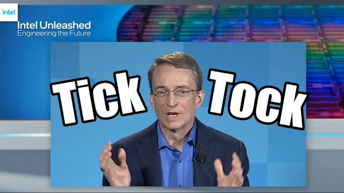
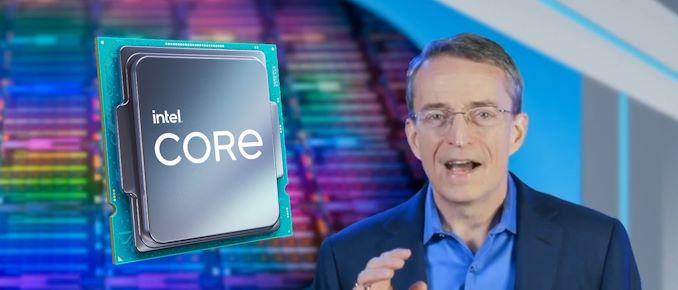
Today Intel’s CEO Pat Gelsinger has outlined two key changes to Intel policy: one derived from Intel’s plans to offer foundry services to external partners, and the other from Intel starting to outsource its core compute product families in order to get the best product at a given time. Not only is Intel set to offer x86 core IP to customers through its new Intel Foundry Services, but also Intel is looking to creating leadership compute products on external nodes. These are complete 180º turns from how Intel has previously operated.


For the last 20-25 years, Intel has been steadfast in keeping the crown jewels of its product design firmly inside its very protective walls. Over the years, Intel’s x86 designs have mostly led the market in leadership performance and power (except for Pentium 4 and Rocket Lake), and limiting use/production for Intel-only use has enabled the company to improve that design with laser focus, manufacturing not-withstanding. Keeping the cores for internal use only means that neither customers nor competitors were able to see the raw design specifications, and for a long time this has enabled Intel to keep key features, such as its branch predictors, away from all but the most prying eyes.


In a twist to the norm, Intel is now set to dissolve those walls keeping its x86 cores it itself.


First up is Intel’s Foundry Services, a second crack at offering external customers the ability to use Intel’s manufacturing facilities. Idle fabs are costly, and so with IFS, Intel wants to enable a revenue stream while at the time meeting global demand for semiconductors, especially as it pertains to local supply chain security and migrating the world’s semiconductor reliance away from Asia more into the USA and EU. IFS will stand as a separate business unit inside Intel.


As part of IFS, Intel will both offer raw manufacturing services, similar to a standard foundry like TSMC and Samsung, as well as its portfolio of IP to customers. This is a Big Deal™.  Intel will enable a fully vertical model with its IP portfolio, allowing customers to choose from x86 cores, graphics, media, display, AI, interconnect, fabric, packaging, and other critical foundational IP from other sources (such as Arm, RISC-V). The exact way in which customers will be able to license the IP will be announced in due course, but if Intel were to follow the Arm model, then Intel customers will get access to Intel’s 86 core designs.


Arm’s model is bidirectional: core IP and architecture IP. The first allows you to build an SoC with defined cores, while the latter allows you to build your own cores with the instruction set (like Apple does with Arm). When applied to Intel, with the core IP, a customer can build designs based on Intel’s x86 cores with their own or external interconnects, or in different configurations to Intel’s standard model that are more optimized for what that particular customer requires. At the minute Intel is set only to offer core IP licenses, not architecture IP licenses.


If we take this idea and extrapolate, we could very well see x86 cores combined with new memory controllers, active interposers with custom interconnects.


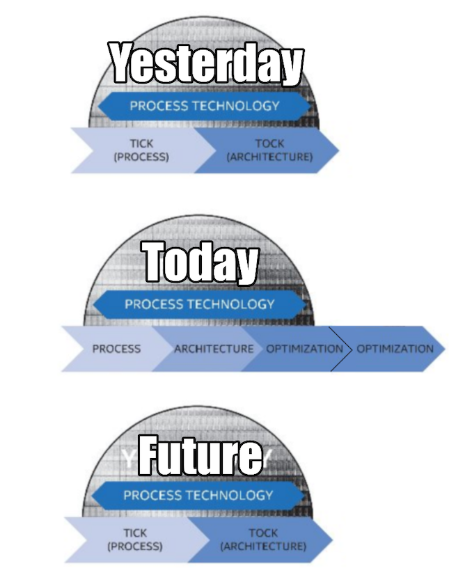
Intel has kind of done this before, although it was very much a walled garden. Intel offered foundry services almost 7 years ago, under then CEO Brian Krzanich, that allowed very select customers to build new SoC designs, with Intel’s help, and only for very select pre-approved use cases. In that time, Intel’s effort for a proper foundry business was, in Gelsinger’s own words, ‘weak’. The new model is set to be more open, as far as we’re led to believe.


The only question becomes to what extent will Intel offer x86 cores. Will it be the latest cores designed internally, or would they be a couple of generations behind? Will those designs be offered on a variety of process nodes, or just on a singular process node? Would a customer be able to get a core IP license and build it at another fab? This is where the second part of the announcement comes in.


As part of today’s announcement, Intel has stated that it will be expanding its use of third-party foundry capacity. Pat Gelsinger highlighted that it would be leveraging its relationships with TSMC, GlobalFoundries, Samsung, and UMC, to enable the best manufacturing facilities for its leading edge product designs, from communications and connectivity to graphics and chiplets. This builds on the announcements made by former CEO Bob Swan last year in light of Intel’s own troubles on its 7nm process. Today’s announcements reaffirms Swan’s messaging, given that at the time the word ‘pragmatic’ was used, so while this has probably been in the works in a while, it is good to get a clear confirmation. As part of this announcement, to quote:


‘Gelsinger said he expects Intel’s engagement with third-party foundries to grow and to include manufacturing for a range of modular tiles on advanced process technologies, including products at the core of Intel’s computing offerings for both client and data center segments beginning in 2023’


The key phrase here is ‘core of Intel’s compute offerings’. It could be interpreted in two ways: at the core of a CPU design is a CPU core, which would mean an x86 design unless Intel were to skew away from x86 (unlikely). The other alternative could be an IO chiplet, which is also a ‘core part’ of a compute offering. Paul Alcorn from Tom’s Hardware has confirmed from Intel that the key element here is ‘compute cores’, and although Intel hasn’t specifically said the ISA of those cores, we are set to believe that Intel does indeed mean x86.


This means that other foundries will have access to the floorplans of Intel’s x86 designs, which used to be a big no-no at Intel. Now in saying that, foundries often have strict NDA requirements that stop them sharing designs with customers, as you might expect, but it’s the fact that Intel is even letting another foundry build x86 cores that is the highlight of this announcement.


All-in-all, Pat Gelsinger is enabling a roadmap that allows Intel to pivot, and pivot hard. Steering the Intel behemoth is difficult at the best of times, however Pat’s arrival and enthusiasm has certainly made the company more comfortable in finding where its next generation of revenue is coming from.


Source: AnandTech – Intel’s x86 Designs No Longer Limited to Intel on Intel: IP Blocks for Foundry, Cores on TSMC

Intel to Revive ‘Tick-Tock’ Model, Unquestioned CPU Leadership Performance in 2024/2025

As part of today’s announcements, during Intel’s Q&A session after the prepared remarks, CEO Pat Gelsinger explained how Intel is going to revive its fortunes when it comes to its leading edge compute products. One of Gelsinger’s mantras seems to be that unquestioned leadership products bring unquestioned leadership margins for those products, and for Intel to execute, it needs to return to its days of old.


In the past, through the 1990s, 2000s, and into the 2010s, Intel’s manufacturing philosophy was known as ‘Tick-Tock’. This means that for every product generation, the leading edge compute hardware was either a Tick (process node enhancement), or a Tock (microarchitecture enhancement). Each generation would alternate between the two, allowing Intel to take advantage of a familiar design on a new process node, or using a mature node to enable a new performance-focused design. That policy was scuppered when delays to Intel’s 10nm forced Intel into more of a Tick-Tock-Optimization-Optimization-Optimization model.


Today CEO Pat Gelsinger stated that at Intel’s core it has to re-establish the Tick-Tock model that enabled repeated leadership in the CPU ecosystem, buoyed by a healthy CPU roadmap. Part of this is re-establishing discipline in Intel’s ranks to continually provide both microarchitecture updates and process node updates on a regular expected cadence. Pat stated as part of the call that Intel will look towards a confirmed yearly process node improvement, and as a result, there might be a lot of Ticks in the future, with a push to more Tocks as well.


On top of this commentary, Pat Gelsinger also stated that Intel’s CPU roadmaps are already baked in through 2021, 2022, and 2023. The company is thus looking to 2024/2025 for ‘unquestioned CPU leadership performance’, which traditionally means the fastest processor for single thread and multi-thread workloads. This is for sure a laudable goal, however Intel will also have to adapt to a changing landscape of chiplet processor designs (coming in 2023), enhancing on-die accelerators (GNA already present), and also what it means to have leadership performance – in the modern era, leadership performance doesn’t mean much if you’re also pushing lots of Watts. Intel stated that its 7nm process is now comfortably on track to deliver Meteor Lake, a client CPU using tiles/chiplets, in 2023, however we are likely looking to a 7nm variant or even external processes for a 2024/2025 product. Intel has also stated that it is looking to consider the core of its leading edge compute on external foundry processes, although one might argue that this doesn’t explicitly say ‘CPU’.


It is also worth noting that Intel/Gelsinger isn’t calling its disaggregated silicon as ‘chiplets’, and prefers to use the term ‘tiles’.  This is because Intel’s tiles amount to long wires across 3D packaging technologies like EMIB and Foveros, compared to package-based multi-die interconnect that require buffers as well as control fabric. Tiles by this definition are more costly to implement than chiplets, and have additional thermal considerations by having high-powered silicon close together, so it will be interesting to see how Intel balances these new packaging technologies with the more cost-sensitive elements of its portfolio, such as client processors.


It’s been known that Intel’s microarchitecture teams haven’t been idle waiting for 10nm to come through the pipe, with a number of designs ready and waiting to go for when the process node technology matures. With any luck, if Intel can get a headwind with 7nm, when 2024 rolls around it might all come thick and fast.


Source: AnandTech – Intel to Revive ‘Tick-Tock’ Model, Unquestioned CPU Leadership Performance in 2024/2025

Intel’s New IDM 2.0 Strategy: $20b for Two Fabs, Meteor Lake 7nm Tiles, New Foundry Services, IBM Collaboration, Return of IDF

The new CEO of Intel, Pat Gelsinger, has today outlined his vision for Intel over the coming years. During an online presentation entitled ‘Intel Unleashed: Engineering The Future’, Pat Gelsinger outlined five key topics upon which Intel will work towards and what it means for the company at large. At the center of this is a reaffirmed commitment for Intel to retain its own fabs, but also double down on its ability to drive the latest technologies at scale by building new manufacturing facilities inside the US.


Source: AnandTech – Intel’s New IDM 2.0 Strategy: b for Two Fabs, Meteor Lake 7nm Tiles, New Foundry Services, IBM Collaboration, Return of IDF

Intel’s DPG Launch Event April 6th: Early Look at 3rd Gen Xeon Scalable (Ice Lake)

Today Intel has announced that it will be holding a launch event on April 6th for the new vision of its Data Platform Group. This event is set to ‘unveil the next chapter’ in all the areas that Intel’s DPG touches, from edge to cloud, as well as offering an early look at 3rd Gen Intel Xeon Scalable systems, which we’ve come to understand is the Ice Lake Xeon platform. Key speakers at the event include Intel’s new CEO, Pat Gelsinger.


How Wonderful Gets Done 2021


Subtly dropped in my email today as part of the Intel weekly on data center progress, the company have announced a ‘How Wonderful Gets Done 2021’ event built upon the Data Platform Group’s progress as well as the vision for the segment of Intel looking to the future. The key headliner, present in our email but not on Intel’s website, is that the event will host an ‘early look at 3rd Gen Intel Xeon Scalable processor-based systems’. It is unclear if this means CPUs or just OEM designs, or if we’ll see benchmarks, but it is clear that Intel’s OEM partners are practically ready to go based on some of the published data already available.


From the email


One of the accompanying videos on the event website is a 10 second montage of things forming the letter ‘X’, and the words ‘what will you solve for’.


The event will be held on Tuesday April 6th, starting at 8am PT, with keynotes from new Intel CEO Pat Gelsinger, EVP and GM of DPG Navin Shenoy, and CVP and GM of the Xeon and Memory Group, Lisa Spelman.


Sessions for the day will include:


  • AI, Wei Li, VP and GM of Machine Learning Performance, Design Engineering Group
  • IoT, John Healy, VP IOTG, GM Platform Management and Customer Engineering
  • 5G Networking, Dan Rodriguez, CVP and GM, Network Platforms Group
  • HPC, Trish Damkroger, VP and GM HPC, Data Platfoms Group
  • Cloud, Rebecca Weekly, VP and GM, Hyperscale Strategy; Senior Principle Engineer, DPG


Recently it was announced that Pat Gelsinger will be hosting an event on March 23rd, and in that announcement an image of an Ice Lake Xeon Scalable wafer was given as the title image for that announcement, perhaps indicating that the release of ICL-SP is close. Intel did say at the beginning of the year that ICL-SP is expected to launch ‘within months’, and a number of Intel’s partners are already starting to demonstrate systems with appropriate processor support.


We also learned recently that Intel has already shipped 115K+ (and more) Ice Lake Xeon Scalable processors to over 30 of its high-profile customers, even though the processors have not yet been launched. This is typical for a server processor, as these customers also help test, debug, and deploy the hardware at scale so it is ready to go from day one.


Similarly, in discussions with Intel, it is clear that the company is keen to promote its combined solution efforts to the market when it comes to the data center – Intel’s value, according to the company, is in its ability to provide the CPU, the networking, the memory, the storage, the AI accelerators, the software, the optimizations, the range of options, and the support structure that its competitors cannot. This combined solution Intel believes affords its customers a better TCO offering, as well as better optimized performance especially now that workloads are hitting a variety of bottlenecks such as storage, connectivity, and acceleration.


We are all set up for the event and will be watching along. If there are opportunities to ask questions, you bet we will.


Source: Intel


Source: AnandTech – Intel’s DPG Launch Event April 6th: Early Look at 3rd Gen Xeon Scalable (Ice Lake)

AI Meets Chipmaking: Applied Materials Incorporates AI In Wafer Inspection Process

Advanced system-on-chip designs are extremely complex in terms of transistor count and are hard to build using the latest fabrication processes. In a bid to make production of next-generation chips economically feasible, chip fabs need to ensure high yields early in their lifecycle by quickly finding and correcting defects.

But finding and fixing defects is not easy today, as traditional optical inspection tools don’t offer sufficiently detailed image resolution, while high-resolution e-beam and multibeam inspection tools are relatively slow. Looking to bridge the gap on inspection costs and time, Applied Materials has been developing a technology called ExtractAI technology, which uses a combination of the company’s latest Enlight optical inspection tool, SEMVision G7 e-beam review system, and deep learning (AI) to qucikly find flaws. And surprisingly, this solution has been in use for about a year now.


Source: AnandTech – AI Meets Chipmaking: Applied Materials Incorporates AI In Wafer Inspection Process

Intel’s New Adaptive Boost Technology: Floating Turbo Comes to Rocket Lake

A couple of days after Intel officially announced its 11th Generation Core Rocket Lake, the press received an email about a new feature coming to the platform that wasn’t in our original briefing. The goal of this feature is to provide more performance to users that have good processors, and Intel is calling it Adaptive Boost Technology.


Source: AnandTech – Intel’s New Adaptive Boost Technology: Floating Turbo Comes to Rocket Lake

Intel Drops Teaser For Upcoming Xe-HPG GPU Architecture

With the launch of their first-iteration Xe-LP architecture now firmly in the proverbial rearview mirror, Intel’s GPU division has turned its sights towards its next consumer-focused GPU architecture, Xe-HPG. Today the company has posted a very light teaser video advertising the forthcoming architecture.


The brief, 30 second promotional video highlights how Xe-HPG is built on top of Intel’s current Xe-LP architecture. And while there aren’t any concrete technical details disclosed within the otherwise abstract video, it’s notable that the video does briefly show 5 layers of blocks on the Xe-HPG chip. Assuming for the moment that Intel isn’t being quite literal here – a 5 layer GPU would be extravagant and hard to cool, to say the least – it’s more likely an allusion to the number of Execution Units (EUs) or some other aspect of the architecture.


Finally, the video also includes a short block of binary text as a further game for the audience to play.


00100011

10100000

11101101

11010000


For the moment we don’t have a solid idea of what it means. But no doubt someone will figure it out before too long.


Otherwise, this will no doubt be the first of many teasers for Xe-HPG. While Intel hasn’t provided a more recent roadmap for chips based on the architecture, the company previously announced in 2020 that they were aiming for a 2021 launch. And with the first DG2 chip already in the labs as of October, we know that Intel is well underway in bringing up Xe-HPG silicon.


Source: AnandTech – Intel Drops Teaser For Upcoming Xe-HPG GPU Architecture

NVIDIA Raises GeForce NOW Paid Subscription Plans to $10 Per Month, $100 Per Year

Just over a year ago, NVIDIA finally brought GeForce NOW, its PC game streaming service, out of beta. The commercial launch of the service saw the introduction of two tiers: a feature and time-limited free tier, and a paid Founders tier that offered a full set of features (including RTX) and priority access. Now as the company is in its second year of operating the commercial service, today NVIDIA is raising the price for GeForce NOW paid subscriptions, essentially doubling them to $10/month (or $100/year) for new members.


Officially, what NVIDIA is doing today with its subscription plans is two-fold. First, the Founders plans, which were advertised as a limited-time offer from the very beginning, are finally being retired and will no longer be offered to new customers. In their place the company is launching a new set of “Priority” memberships, which are otherwise identical to the old Founders plans, offering the same features and priority access.


The only meaningful change, other than the name on the plan, will be the price. Whereas the Founders plans were $5 a month or $25 for a six-month subscription, GeForce NOW Priority subscriptions will be sold on a monthly or yearly basis. Monthly plans are now $10 per month (or more specifically, $9.99), while yearly plans are $100 ($99.99).


With that said, as a thank you to their Founders members – and no doubt mindful of the negative public reaction to price hikes – NVIDIA is also grandfathering in the old Founders rate for existing customers under what they are calling their “Founders for Life” benefit. This means that while new customers will have to pay the new, higher prices, existing customers will have their old prices locked in so long as they remain in what NVIDIA calls “good standing.” Which for all practical purposes works out to a 50% discount on the service for existing members.


Past that, NVIDIA’s blog post announcing the price increase doesn’t go in to any detail on explaining the reason for the increase. But it’s not terribly surprising to see NVIDIA raising prices; even without the explicit limited-time nature of the founders packages, $5/month was probably not covering all of NVIDIA’s costs, especially as evidenced by the price of comparable high-end instances from the major cloud service providers. If nothing else, this is a sign that NVIDIA is finally looking to make a real profit from the service, rather than just trying to cover costs.


Overall, NVIDIA seems rather bullish on the future of their unique cloud gaming service, even with the licensing-related teething issues over the past year and the hit to demand that will no doubt come from a price hike. According to the company they’re continuing to add capacity to the service, including spinning up a data center in Montreal later this year. Similarly, the company is continuing to expand its GeForce NOW Alliance partnerships for other countries, further increasing the number of countries that have local GeForce NOW servers.


Finally, while today’s news is largely focused on the business-side of the service, NVIDIA does mention that an upcoming update to the service is going to address refresh rate synchronization. With the 2.0.28 update, the server-side refresh rate will be set to match the client-side refresh rate in order to account for the existence of both 60Hz displays and 59.94Hz displays. This small variance in refresh rates is not an issue with games locally, but similar to streaming video, it can be a problem with cloud gaming as a mis-match would lead to judder and the occasional dropped frame.


Source: AnandTech – NVIDIA Raises GeForce NOW Paid Subscription Plans to Per Month, 0 Per Year

Intel CEO Pat Gelsinger To Host Webcast About Intel’s Future On March 23rd

Intel today has announced that the company will be holding an event on March 23rd to discuss the future of engineering at the company. Dubbed “Intel Unleashed: Engineering the Future”, the hour-long webcast will be hosted by recently hired CEO (and Intel returnee) Pat Gelsinger.


Join Intel CEO Pat Gelsinger for a business update and webcast address on the new era of innovation and technology leadership at Intel.


While Intel’s official description is short and at a high level, given the subject matter and the fact that the presentation is scheduled for after the stock markets close, we’re expecting that this will be Intel’s much-awaited announcement on the future of the company’s manufacturing plans. For the last several months the company has been juggling the question of when and where to use third-party foundries versus investing in their own manufacturing technologies. Intel’s 7nm problems have become a black eye for the company, and the prolific processor producer has been under pressure from some investors to cut back on expensive R&D and just use pure-play foundries like TSMC.


Prior to Intel hiring Gelsinger to be their new CEO in mid-January, the company had been preparing to detail its future foundry plans in its January 21st earnings call. However after bringing Gelsinger on board, that announcement was put on hold to give Gelsinger a time to get up to speed, and possibly make his own mark if he decided to take the company in a different direction than then-CEO BoB Swan was preparing to go.


If this does turn out to be a detailed disclosure of Intel’s foundry plans, then it’s not an exaggeration to say that this webcast will be one of the most critical Intel presentations in years. Gelsinger and the rest of Intel’s upper management have some very difficult choices to make about manufacturing, and no matter what direction they opt to take on Tuesday, it’s going to have significant ramifications for not only Intel, but the rest of the silicon foundry industry as a whole. So tech enthusiasts and investors alike are going to be paying close attention to this announcement.


Source: AnandTech – Intel CEO Pat Gelsinger To Host Webcast About Intel’s Future On March 23rd

Noctua Announces First Cooler in Redux Series, NH-U12S Redux

One of the most popular air cooling brands, Noctua, has announced the first CPU cooler in its highly anticipated Redux series, the NH-U12S Redux. The Redux series is designed to offer a streamlined and more affordable entry point to some of Noctua’s most popular (and sometimes expensive) CPU coolers. Noctua also launches its NA-FK1 Redux second cooling fan kit as an optional extra.


Focusing on the new NH-U12S Redux, Noctua has ‘streamlined’ its previous NH-U12S cooler by opting for a four heat pipe design instead of five on the previous version. Another difference is that Noctua has opted out of a soldered interface between the heat pipes and the cooling fins and supplies just one NF-P12 Redux 120 mm cooling fan to reduce overall costs.


Noctua also has one of the simplest and most popular mounting kits in recent times, with its SecuFirm2 mounting system, with support for LGA11xx, LGA15xx, LGA20xx, as well as Intel’s latest LGA1200 socket. The SecuFirm2 mounting kit also supports AMD’s AM4 socket. The new Redux series has also stripped away some of the unnecessary fluff to allow a lower entry-point for users on a budget but still looking for similar quality and performance levels.


In addition to the NH-U12S Redux, Noctua has made an optional 120 mm fan kit for systems that demand more cooling performance, the NA-FK1 Redux. The NA-FK1 kit includes one matching NF-P12 Redux 1700 rpm cooling fan, with four grey anti-vibration pads, a pair of fan mounting clips, a 4-pin PWM Y-cable, and two NA-RC14 low-noise adaptors. Where the original NH-U12S comes supplied with both cooling fans, the Redux series gives users the option to purchase this separately, which lowers the cooler’s overall cost.


To increase its products’ longevity, Noctua includes its NH-U12S Redux in its future mounting upgrade scheme, which allows users to request a new mounting kit if a new socket is announced cooler can officially support. Noctua is a little vague in specifying if this service is free of charge and states that as long as it’s technically possible for them to do so, it could make the NH-U12S Redux a good long-term investment for a current build and future upgrade paths.


Amazon (US) Link


Noctua also includes a 6-year limited warranty with the NH-U12S Redux and has set an MSRP of $50 and €50, with stock available at its official Amazon store from today. The additional NA-FK1 Redux 120 mm fan kit is also available today and has an MSRP of $17/€17.


Source: Noctua


Related Reading


Source: AnandTech – Noctua Announces First Cooler in Redux Series, NH-U12S Redux

AMD Set To Roll Out AGESA firmware USB Fix For Ryzen, Coming April

Last month, we reported that AMD had been made aware of many users experiencing intermittent connectivity issues with USB ports on its Ryzen 500-series motherboards. Requesting that users with any USB drop-out issues reach out directly to them, AMD has now released a statement confirming that it’s planning to release a firmware update via a new AGESA update.


A post on Reddit by the official AMD account, u/AMD, has revealed that AMD will distribute a new firmware update named AGESA 1.2.0.2 to its motherboard partners within a week. AGESA (AMD’s Generic Encapsulated System Architecture) is AMD’s primary base on which motherboard vendors build their firmware around. This means it’s likely that an update alleviating users with problematic and intermittent USB issues isn’t far away.


AMD’s official statement on its new updated AGESA reads as follows:


We would like to thank the community here on r/AMD for its assistance with logs and reports as we investigated the intermittent USB connectivity you highlighted. With your help, we believe we have isolated the root cause and developed a solution that addresses a range of reported symptoms, including (but not limited to): USB port dropout, USB 2.0 audio crackling (e.g. DAC/AMP combos), and USB/PCIe Gen 4 exclusion.


AMD has prepared AGESA 1.2.0.2 to deploy this update, and we plan to distribute 1.2.0.2 to our motherboard partners for integration in about a week. Customers can expect downloadable BIOSes containing AGESA 1.2.0.2 to begin with beta updates in early April. The exact update schedule for your system will depend on the test and implementation schedule for your vendor and specific motherboard model. If you continue to experience intermittent USB connectivity issues after updating your system to AGESA 1.2.0.2, we encourage you to download the standalone AMD Bug Report Tool and open a ticket with AMD Customer Support.


Randomized USB disconnects can present many issues for a variety of users, with reports of USB capture devices cutting out while recording and problems with VR headsets that primarily rely on its power from USB ports. This also stretches to mouse and keyboard input issues which can also cause an inconvenience to end-users. 


Despite AMD admitting that there is an underlying issue surrounding USB ports on its Ryzen 5000 and Ryzen 3000 processors when used with 500 and 400-series motherboards, it hasn’t gone into details about the fix. They believe they have identified the root cause of the issues, and the new AGESA 1.2.0.2 firmware should begin rolling out sometime in April.


Source: r/AMD


Related Reading


Source: AnandTech – AMD Set To Roll Out AGESA firmware USB Fix For Ryzen, Coming April