Enmotus MiDrive: Rethinking SLC Caching For QLC SSDs

For consumer storage, CES 2020 brought a new wave of competition for PCIe 4.0 SSDs and promise of faster portable SSDs, but the most intriguing product demo was from Enmotus. They are planning a profound change to how consumer SSDs work, ditching drive-managed SLC caching in favor of host-managed tiered storage.


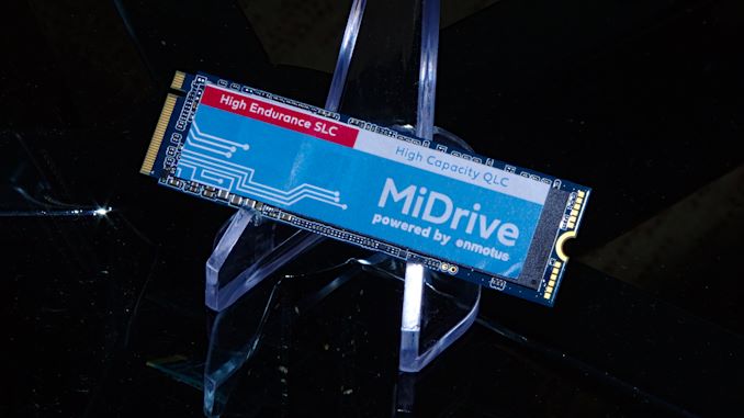
Enmotus is a well-established provider of storage management software. Their most familiar product to consumers is probably FuzeDrive, a limited edition of which is bundled with recent generations of AMD motherboards as AMD StoreMI. This serves as AMD’s answer to Intel’s Smart Response Technology (SRT) and Optane Memory storage caching systems. Enmotus also has enterprise-oriented products in the same vein. Their new MiDrive technology builds on their existing tiering software to manage a combination of SLC and QLC NAND on a single consumer SSD.


Caching and Tiering Challenges


All software-driven caching or tiering solutions tend to have limited consumer appeal due to the complexity of setting up the system. At least two physical drives are required, and the OS needs to load an extra driver to manage data placement. Any compatibility issue or other glitch can easily render a PC unbootable, and data recovery isn’t as straightforward as for a single drive. These hurdles don’t scare off enthusiasts and power users, but PC OEMs aren’t eager to market and support these configurations. But without some form of caching or tiering, consumer SSDs would be limited to the raw performance of TLC or QLC NAND. SLC caching managed transparently by the SSD’s firmware has been adopted by almost all consumer SSDs in order to improve burst performance, and it has proven to be very effective for consumer workloads. The fundamental limitation of this strategy is that the SSD must work with limited information about the nature and purpose of the user data it is reading and writing.


Most SSDs rely on fairly simple procedures for managing their SLC caches: sending all writes to the cache unless it’s full, and using idle time to fold data from SLC into more compact TLC representation, freeing up cache space for future bursts of writes. There are still some choices to be made in implementing SLC caching for consumer SSDs: whether to use a fixed-size cache or dynamically sized, and whether to stall when the cache fills up or divert writes straight to TLC/QLC. As QLC drives become more common, we’re also seeing drives that prefer to keep data in the SLC cache long-term until the drive starts to fill up, so that the cache can help with read performance in addition to write performance.


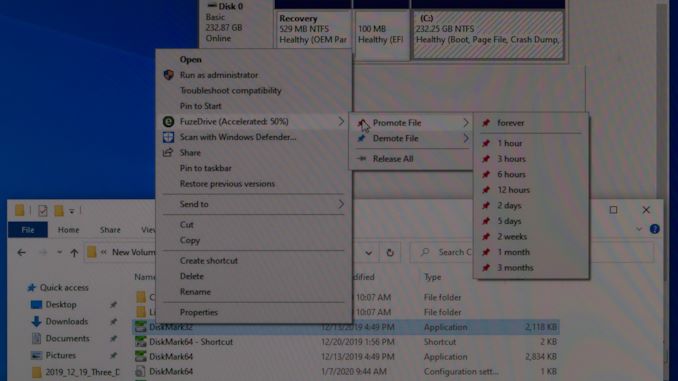
Enmotus FuzeDrive manual data placement controls


Host-managed caching or tiering opens the door to more intelligent management of data placement, since the host OS has better information: about which chunks of data belong to what file, and about the processes and users that interact with those files. It is easier for the host OS to accurately track the history of access patterns for hot vs. cold files. It is also possible to expose manual control of data placement directly to the user.


Two Drives In One


The Enmotus MiDrive technology allows one SSD to present the host with access to two separate pools of flash storage: QLC and SLC managed by the same SSD controller. To implement this, they have partnered with Phison to modify SSD controller firmware. For server products, a single NVMe SSD would expose two separate NVMe namespaces that Linux treats as different block devices. But for consumers, Enmotus has chosen to maximize backwards compatibility by having the MiDrive present itself as a single block device, with the first 32 or 64 GB initially mapped to SLC NAND and the rest of the drive mapped to QLC NAND. This makes it possible (and fast!) to install an OS to a MiDrive without needing any special Enmotus software or drivers. Once the Enmotus driver has been loaded, it takes over the management of data placement using vendor-specific commands that instruct the SSD to promote or demote ranges of Logical Block Addresses (LBAs) between the QLC and SLC pools of flash. (The initialization process for this tiering currently takes about a quarter of a second, because very little data needs to be moved until there’s history indicating what should be in QLC vs SLC.)


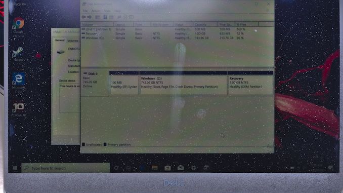
Enmotus MiDrive 800GB appearing as a single device


This is a lot simpler for the host side than the strategy Intel uses for their Optane Memory H10, which is two separate PCIe devices on one M.2 card and requires special motherboard support to properly detect both halves before the caching software can even get involved. Enmotus is working to make MiDrive even simpler by having Microsoft distribute the Enmotus driver with Windows, so that a MiDrive will be automatically detected and managed by the Enmotus software without requiring any user intervention. For now, Windows will default to using its standard NVMe driver for a MiDrive, but that should change by the time products hit the shelves.


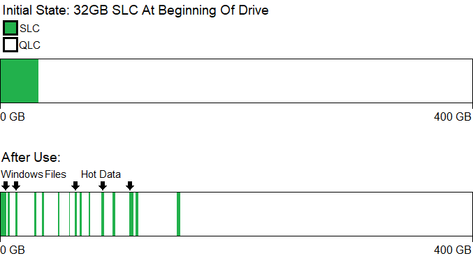
Example of how MiDrive LBA allocation will change with use
(for illustration purposes only, not based on real testing)


Enmotus supports assigning data to SLC or QLC in 4MB chunks, which is probably the size of a single NAND flash erase block in SLC mode, and thus the smallest chunk size that can easily be remapped between the QLC and SLC portions of the drive without contributing to unnecessary write amplification. That 4MB block size means that a small file moved to SLC is likely to bring along other nearby files, which will often contain related data that may also benefit from being in SLC. It also means that large files can be partially resident in SLC and partially in QLC. Since this process doesn’t change the logical block addresses a file occupies, Enmotus MiDrive doesn’t need to change anything about how NTFS organizes data, and it doesn’t need to behave like an advanced disk defragmenter that tries to move important data toward the beginning of the disk. The MiDrive software only needs to look up what LBAs are used by a file and tell the SSD whether to move that data to SLC or QLC blocks. The only side-effect visible to the rest of the OS is a change in the performance characteristics for accessing that part of the SSD.


The SLC portion of an Enmotus MiDrive differs from a traditional SLC cache not only by being host-managed, but also in how the SSD treats it for wear leveling purposes. A typical SSD’s SLC cache may have a static or dynamic size, but in either case when new write commands arrive the SSD will write the data to whatever NAND flash block is currently empty. When the cache is flushed, data from several SLC blocks will be rewritten in TLC or QLC mode to a different empty block, and the SLC blocks are then free to be erased and put back into the pool of available blocks. Managing just one pool of empty blocks means that the actual physical location of the SLC cache can move around over time, and a block that was last used as TLC might end up being used as SLC the next time data is written to it.


By contrast, Enmotus MiDrive technology has the SSD track two entirely separate pools. When the drive is manufactured, the SLC portion is permanently allocated for the lifetime of the drive. Any physical NAND pages and blocks that are used as SLC will always be treated as SLC for the lifetime of the drive, and the same for the QLC portion. The two pools of flash are subject to completely independent wear leveling, even though SLC and QLC portions will exist side by side on each physical flash chip on the drive. This means that the QLC blocks will never be subjected to the short-term Program/Erase cycles of SLC cache filling and flushing. For the SLC blocks, the error correction can be tuned specifically to SLC usage, and that allows Enmotus to achieve around 30k Program/Erase cycles for the SLC portion of the drive (based on Micron QLC NAND). MiDrives will expose separate SMART indicators for the SLC and QLC portions of the drive, so monitoring software will need to be updated to properly interpret this information.


In principle, it would be possible for either the SLC or QLC portion of the drive to be worn out prematurely, but in practice Enmotus is confident that their tiered storage management software will lead to longer overall drive lifespans than drive-managed SLC caching. Files that are known to be frequently modified will permanently reside on SLC and not be automatically flushed out to QLC during idle time. If the Enmotus software is smart enough, it will also be able to determine which files should skip the SLC and go straight to QLC until it becomes clear that a file is frequently accessed. For example, a file download coming into the machine over gigabit Ethernet will not initially need SLC performance because raw QLC can generally handle sequential writes at that speed (especially with no background SLC cache flushing to slow things down). And if that file is a movie which is infrequently accessed and only read sequentially, there’s no reason for it to ever be promoted up to SLC. In general, the tiered storage management done by Enmotus should result in less data movement between SLC and QLC, rather than the increased write amplification that traditional SLC caching causes.


Since the SLC portion of an Enmotus MiDrive is a slice carved out of regular QLC NAND, it cannot offer all the benefits of specialized low-latency SLC NAND like Samsung’s Z-NAND or Kioxia/Toshiba XL-Flash. The SLC portion of a MiDrive won’t be appreciably faster than the SLC cache of a traditional consumer SSD, but that performance will be more consistent and predictable when working with files that are kept entirely on the SLC portion of the drive.


The Business Model


Enmotus MiDrive is currently implemented as a combination of Windows driver software and custom SSD firmware for Phison NVMe controllers, but it does not require any custom hardware. This means that any vendor currently selling Phison E12 NVMe SSDs can make a MiDrive-based product by licensing and shipping Enmotus firmware. PC OEMs can adopt MiDrives by switching to drives with Enmotus firmware and ensuring that they either include the Enmotus drivers in their Windows images, or relying on them to be distributed through Windows Update. No motherboard firmware or hardware modifications are required, or any changes to the process of provisioning a machine and preparing it for delivery to the end user. Enmotus is engaging both with PC OEMs and vendors of retail SSDs, so we can expect pre-built systems with Enmotus MiDrive technology and and upgrade options usable on any Windows 10 PC that already supports standard M.2 NVMe SSDs. Enmotus is optimistic about uptake from PC OEMs, expecting MiDrive to get a much better reception than Intel’s Optane H10 did.


The basic MiDrive products will be fully automatic, with the Enmotus driver pre-installed or installed automatically when a MiDrive is detected. Data placement decisions will be completely behind-the-scenes. For enthusiasts, there will also be a premium tier similar to their current FuzeDrive software, which includes Windows Explorer shell integration so that individual files can be manually promoted or demoted, either permanently or for a limited period of time. Enmotus will also be providing a drive health monitoring tool that will include their estimate for how much extra drive lifetime has been won by using their tiering instead of ordinary SLC caching.


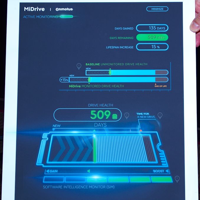
Mockup of Enmotus MiDrive SSD health monitoring tool


Enmotus expects SSDs with MiDrive technology to mostly use either 32GB or 64GB SLC portions and offer total capacities from about 400GB up to around 2TB, but the exact configurations will be determined by what their partners want to bring to market. Enmotus is also planning enthusiast-oriented solutions supporting RAID-0 style striping across multiple physical drives, and solutions for single-package BGA SSDs that go into small form factor and embedded devices.


Enmotus MiDrive technology will add to the price of SSDs, but since we’re talking about QLC storage that’s only relative to the cheapest NVMe SSDs available, and the final sticker prices will still be competitive for consumer SSDs. In return for that, users should get better real-world performance and enough effective write endurance to justify a 5-year warranty. We’re looking forward to testing out this technology later this year, even though it will further complicate our benchmarking process. Enmotus is already sampling to interested OEMs.


Source: AnandTech – Enmotus MiDrive: Rethinking SLC Caching For QLC SSDs

Crucial’s 32 GB UDIMMs and SODIMMs Available: DDR4-2666 & DDR4-3200

In the summer of 2019, Crucial was among the first brands to demonstrate 32 GB unbuffered memory modules, which were based on Micron’s 16 Gb DDR4 chips. Now after a bit of a wait, those 32 GB UDIMMs as well as 32 GB SO-DIMMs have finally hit the retail market.


Crucial’s 32 GB unbuffered DIMMs and SO-DIMMs are rated for DDR4-2666 with CL19 at 1.2 V and DDR4-3200 with CL22 at 1.2 V operation. The modules are not equipped with any heat spreader and since they operate in JEDEC-standard modes, they are compatible with a wide variety of PCs that can support 32 GB UDIMMs in general.


At present, Crucial’s 32 GB UDIMMs and SO-DIMMs are available as 64 GB dual-channel memory kits priced at around $330 at the company’s website. Interestingly, the faster DDR4-3200 kits are only $2 more expensive than the slower DDR4-2666 kits. Meanwhile, Amazon.com expects Crucial’s 64 GB dual-channel DDR4-2666 SO-DIMM kit to arrive on February 3, 2020.


It is unclear why Crucial did not start selling its 32 GB UDIMMs and SO-DIMMs to general public earlier, as there are a number of brands that have been offering competing 32 GB UDIMMs using the same Micron chips for months now. In any case, Crucial’s 32 GB DIMMs are finally available.


Related Reading:


Sources: Crucial


Source: AnandTech – Crucial’s 32 GB UDIMMs and SODIMMs Available: DDR4-2666 & DDR4-3200

Matrox Unveils D-Series Graphics Cards with NVIDIA Quadro GPUs

Matrox Graphics is one of the oldest graphics card manufacturers still in business today. It started to make video cards in 1978, several years before ATI, and 15 years before NVIDIA. While the company’s own internal GPU development efforts petered early this century, the company has continued on as a specialist card maker, using other vendors’ GPUs to make special-purpose multi-monitor solutions. Since 2014 the company has been using AMD’s GPUs for its boards, and earlier this month the company inked a similar agreement with NVIDIA. This week, Matrox launched its first NVIDIA-based graphics cards.


The Matrox D-series family of multi-display graphics cards based on a custom-built NVIDIA Quadro embedded GPU and carries 4 GB of GDDR5 memory as well as four DisplayPort 1.4 (D1480) or four HDMI 2.0 (D1450) outputs. The D1450 supports four monitors, with a maximum resolution of up to 4096×2160@60Hz, whereas the D1480 adapter supports four monitors with resolujtions up to 5120×3200@60Hz. The card consumes 47 W and only uses power supplied to it through the PCIe x16 slot.


For video wall applications used in aerospace, military, pro A/V, digital signage, security, and industries, four of Matrox D-series boards can be combined in a single system via board-to-board framelock cables, driving up to 16 displays using one PC. In addition, the cards can further be augmented with Matrox’s QuadHead2Go multi-display controllers to drive up to 64 Full-HD screens from a single PC. It is also possible to pair D-series cards with Matrox Mura IPX capture and IP encode/decode boards for applications that need those capabilities.


Matrox does not disclose which GPU it uses for the D-series video cards, but it claims that the ‘custom-built’ NVIDIA Quadro GPU is compatible with DirectX 12, OpenCL 1.2 and OpenGL 4.5, which points to one of NVIDIA’s latest architecture (e.g., Pascal, Turing).


Matrox’s D1450 and D1480 graphics cards will be available sometimes in the second quarter. Their exact pricing is unknown, but expect to see Matrox to charge a premium for their specialized products.


Related Reading:


Sources: Matrox Graphics, Matrox Graphics


Source: AnandTech – Matrox Unveils D-Series Graphics Cards with NVIDIA Quadro GPUs

Zhaoxin’s x86-Compatible CPUs for DIY Enthusiasts Now Available

Zhaoxin, a joint venture between Via Technologies and the Chinese government, has been selling processors for various client systems for years, but recently the company rolled out its latest CPUs that some of the local PC makers position as solutions for DIY enthusiasts. At least initially, Zhaoxin’s KaiXian KX-6780A will be available only in China.


Zhaoxin’s KaiXian KX-6780A is an eight-core x86-64 processor with 8 MB of L2 cache, a dual-channel DDR4-3200 memory controller, modern I/O interfaces (PCIe, SATA, USB, etc.), and integrated DirectX 11.1-capable graphics (possibly S3 based but unknown). The CPU cores are in-house designed LuJiaZui cores, built around a superscalar, multi-issue, out-of-order microarchitecture that supports modern instruction sets extensions like SSE 4.2 as well as AVX along with virtualization and encryption technologies. The processor is made using TSMC’s 16 nm process technology.


Zhaoxin formally introduced its KaiXian KX-6000-series CPUs back in 2018, but it looks like higher-end models like the KX-U6780A and the KX-U6880A are entering the consumer market this quarter.


As it turns out, Xinyingjie, one of Chinese PC makers, uses the C1888 motherboard based on the KX-U6780A that is designed for enthusiast-grade PCs and therefore supporting expandability using a PCIe 3.0 x16 slot, two SO-DIMM slots, M.2 slots, and various internal and external interfaces. One thing to keep in mind about the Zhaoxin’s KaiXian KX-6780A/C1888 platform is of course lack of CPU upgrade path because the processor uses an BGA packaging.


When Zhaoxin originally introduced its Kaixian KX-6000, it said that their performance was comparable to that of Intel’s 7thGeneration Core i5 processor, a quad-core non-Hyper-Threaded CPU. Since then, we have not really got a proper confirmation to the claim and will certainly be interested to test the chip in our labs.


According the to the video source, this mini-PC design is expected to be available from March for consumers. Currently this is a prototype, with enhancements expected between now and the final product.


Should anyone from Zhaoxin (or Xinyingjie) be interested in getting a full review of the product, please reach out to our senior editor Dr. Ian Cutress, at ian@anandtech.com. We’re really interested in testing it.


Related Reading:


Source: 二斤自制 YouTube Channel


Source: AnandTech – Zhaoxin’s x86-Compatible CPUs for DIY Enthusiasts Now Available

Cooler Master MasterAir G200P Super Low Profile RGB Cooler: 39.4mm for 95W

Cooler Master has introduced its new CPU cooler for small form-factor PCs. The MasterAir G200P is 39.4 mm tall, and CM claims it features an advanced heatsink, a relatively quiet fan, and addressable RGB LEDs that enable modders to build attractive compact desktops.


The MasterAir G200P measures 95×92×39.4 mm (3.7×3.6×1.6 inch) and features an aluminum base plate with over 50 fins and two C-shaped heat pipes as well as a copper base. The cooler is equipped with a 92-mm PWM fan with RGB lighting that features a rotational speed between 800 and 2,600 RPM ± 10% and can generate up to 35.5 CFM air flow and up to 26 dBA noise.


Cooler Master’s MasterAir G200P is compatible with all modern processor sockets from AMD and Intel, though the manufacturer does not disclose a ‘maximum’ TDP, but does rate the cooler for use with 95 W CPUs. Typically, low-profile CPU coolers that are around 30 mm tall are rated for CPUs with a 35 W ~ 65 W TDP, but the MasterAir G200P is slightly taller and has heat pipes, so the manufacturer rates it for 95 W processors. 


One of the key selling points of the MasterAir G200P is its addressable RGB lighting that can be controlled using software from leading motherboards makers.


The Cooler Master MasterAir G200P Specifications
  MAP-G2PN-126PC-R1
CPU TDP 95 W
Material Copper base, aluminum fins
Dimension with Fan 95 mm (W) × 39.4 mm (H) × 92 mm (D)
Heat Pipes 2 × C-shaped heat pipes
Air Pressure ~ 2.4 mm H2O
Air Flow (CFM) 35.5 CFM
Speed  800 ~ 6600 ± 10% RPM
Noise 6 ~ 28 dBA
Type of Bearing ?
Life Expectancy 40,000 hours at unknown temperature
Weight ? grams
Compatibility AMD AM4/FM2+/FM2/FM1/AM3+/AM3/AM2+/AM2
Intel LGA1151/1150/1155/1156

Cooler Master’s MasterAir G200P is immediately available from leading retailers like Amazon at an MSRP of $44.99. The device is covered with a two-year limited warranty.


Related Reading


Source: Cooler Master


Source: AnandTech – Cooler Master MasterAir G200P Super Low Profile RGB Cooler: 39.4mm for 95W

Quick Notes: Navi Refresh and RDNA2 Both In 2020, According to AMD

As part of today’s FY2019 earnings call, AMD CEO Dr. Lisa Su had a few words to say about AMD’s future GPU plans – an unexpected nugget of information since we weren’t expecting AMD to reveal anything further at this time.


In short, for this year AMD is planning on both Navi product refreshes as well as parts based on the forthcoming RDNA 2 GPU architecture. To quote Lisa Su:


In 2019, we launched our new architecture in GPUs, it’s the RDNA architecture, and that was the Navi based products. You should expect that those will be refreshed in 2020 – and we’ll have a next generation RDNA architecture that will be part of our 2020 lineup. So we’re pretty excited about that, and we’ll talk more about that at our financial analyst day. On the data centre GPU side, you should also expect that we’ll have some new products in the second half of this year.


All told, it looks like AMD is setting themselves up for a Vega-like release process, launching new silicon to replace their oldest existing silicon, and minting new products based on existing and/or modestly revised silicon for other parts of their product stack. This would be very similar to what AMD did in 2017, where the company launched Vega at the high-end, and refreshed the rest of their lineup with the Polaris based Radeon RX 500 series.


AMD’s GPU Roadmap As Of July 2019


But as always, the devil is in the details. And for that, we’ll have to stay tuned for AMD’s financial analyst day in March.


Source: AnandTech – Quick Notes: Navi Refresh and RDNA2 Both In 2020, According to AMD

NZXT Unveils Kraken X-3 and Kraken Z-3 Series Closed-Loop CPU Coolers

NZXT has introduced its new Kraken X-3 and Kraken Z-3 closed-loop CPU coolers. The coolers are compatible with all modern platforms and are based on Asetek’s latest pumps, offering a blend between performance and quiet operation. Like all modern hardware for enthusiasts, the look of the coolers can be customized using the company’s proprietary software.


The new NZXT Kraken X-3 series includes 240 mm, 280 mm, and 360 mm radiator models, while the more expensive NZXT Kraken Z-3 family is comprised of a 280 mm and a 360 mm SKUs. All five closed-loop coolers are based on Asetek’s 7th Generation pump, which uses a 800 – 2,800 RPM motor. Paired with the Asetek pump are NZXT’s Aer P120 fans, which offer an operational range from 500 to 2,000 RPM and are rated to generate 21 dBA – 36 dBA of noise. The cooling systems use rubber tubing with a nylon braided sleeve as well as caps with a 360° rotation orientation feature, so that the cap can be installed in any direction.


The more affordable NZXT Kraken X-3 comes with a 10% bigger LED ring (when compared to previous models) with a rotable top featuring the company’s logotype. The more expensive NZXT Kraken Z-3 has a 2.36-inch LCD screen that can display various useful information (or just a picture) in 24-bit color, thus allowing to completely customize the look of the cooler.


As for compatibility, the new all-in-one coolers from NZXT can work with all modern CPUs from AMD and Intel, including those that use mainstream AM4 or LGA1155 form-factors as well as HEDT CPUs featuring LGA2066 and TR4 packages.


Specifications of NZXT Kraken X3 & Kraken Z3 Cooling Systems
  General Specifications
Fan (single) Speed (RPM) 500-2,000±300 RPM
Airflow (CFM) 18.28 – 73.11 CFM
Static Pressure (mm-H2O) 0.18 ~ 2.93 mm-H2O
Noise (dBA) 21 – 36
Power 3.84 W
MTBF (hrs) ≧60,000 @ unknown oC
Connector 4-pin PWM connector
Pump Speed (RPM) 800 – 2,800±300 RPM
Life Expectancy ? @ unknown oC
Power 4.8 W
Tubing Length 400 mm
Compatibility AMD AM4, TR4
Intel LGA 1151, 1150, 1155, 1156, 1366, 2011, 2011-3, 2066
TDP ? W

NZXT’s latest Kraken X-3 and Kraken Z-3 closed-loop CPU coolers are immediately available in the USA directly from the company and will be launched in other countries next month. The cheapest Kraken X53 carries an MSRP of $129.99, whereas the most expensive Kraken Z73 is priced at $279.99.


NZXT Kraken X-3 and Kraken Z-3 Coolers
  Size MSRP
Kraken X53 240 mm $129.99
Kraken X63 280 mm $149.99
Kraken X73 360 mm $179.99
Kraken Z63 280 mm $249.99
Kraken Z73 360 mm $279.99


Related Reading:


Source: NZXT


Source: AnandTech – NZXT Unveils Kraken X-3 and Kraken Z-3 Series Closed-Loop CPU Coolers

VAIO Launches SX12: A 12.5-Inch Ultralight Laptop with a Six-Core Comet Lake CPU

VAIO has unveiled a new version of its SX12 laptop that is powered by Intel’s Comet Lake processor, offering SKUs with up to six CPU cores. The miniature notebook weighs less than a kilogram and should not only offer decent performance, but also has a vast set of connectors as well as an optional 4G/LTE modem.


To minimize its weight and dimensions, the VAIO SX12 comes in an enclosure that is made of carbon fiber and plastic. As a result, the machine weighs just 906 grams and is 15.7 mm ~ 18 mm thick. The notebook features a Full-HD display with very thin bezels that allowed VAIO to install a 12.5-inch screen into an 11-inch-class chassis. Furthermore, the company has managed to equip its SX12 with a keyboard featuring a 19-mm pitch.


The 2020 VAIO SX12 is based on Intel’s 10th Generation Core i5-10210U and Core i7-10710U processors, which offer four or six CPU cores as well as built-in UHD Graphics. The CPU is paired with 8 GB of LPDDR3 memory as well as a 256 GB SSD with a PCIe or SATA interface. Like other PCs from VAIO, the new SX12 fully supports the company’s TruePerformance technology that combines an advanced cooling system as well as increased CPU power limits in order to enable the CPU to work at higher clocks for a longer time.


Like previous-generation VAIO SX12, the new notebook has a set of connectors typically not found on 12-inch class machines. In particular, the laptop has GbE, a USB 3.1 Gen 2 Type-C (can be used for data, display, and charging) port, one USB 3.1 Gen 2 Type-A connector, two USB 3.0 Type-A ports, an SD card reader, two display outputs (HDMI, D-Sub), a 3.5-mm audio jack, and a proprietary power port. As for wireless technologies, the notebook is equipped with a Wi-Fi 5 + Bluetooth 4.1 controller as well as an optional 4G/LTE modem. In addition, it has a webcam with IR sensors for face recognition, a fingerprint reader, stereo speakers, and a microphone.


VAIO says that the SX12 can work for 13.2 – 13.5 hours on one charge, but does not disclose exact capacity of the battery. Meanwhile, the system can be charged using a proprietary power brick, or a standard USB-C charger.


VAIO SX12 (VJS1211) General Specifications
  VJS12290111B

Black
VJS12290211B

Black
VJS12290311B

VJS12290411T

Brown
Display 12.5″ anti-glare panel with 1920×1080 resolution
SoC Core i7-10710U

(6C/12T, 1.1 ~ 4.7 GHz)
Core i5-10210U (4C/8T, 1.6 ~ 4.2 GHz)
RAM 8 GB LPDDR3
Storage 256 GB NVMe 256 GB SATA
Wireless  802.11ac Wi-Fi

Bluetooth 4.1

Optional 4G/LTE modem
 802.11ac Wi-Fi

Bluetooth 4.1
I/O ports GbE

1 × USB 3.1 Gen 2 Type-C

1 × USB 3.1 Gen 2 Type-A

2 × USB 3.0 Type-A

HDMI

D-Sub

SD Card reader (UHS-I)
Camera 720p webcam
Audio Integrated speakers

1 × TRRS 3.5-mm jack for headset
Dimensions 287.8 × 203.3 × 15.7 ~ 18 mm
Weight 887 ~ 906 grams
Battery 13.2 ~ 13.5 Hours
OS Windows 10
Fingerprint Yes
Availability January 2019

The new VAIO SX12 laptops will be available in five colors, including black, silver, brown, pink, and red for a custom special edition model. In Japan, the new PCs will cost ¥197,800 – ¥242,800 depending on configuration. Unfortunately, it is unclear when the new SX12 is set to become available in the US, if at all.


Related Reading:


Sources: VAIO, PC Watch


Source: AnandTech – VAIO Launches SX12: A 12.5-Inch Ultralight Laptop with a Six-Core Comet Lake CPU

Assassin’s Speed: Eve Technology Reveals 27-Inch QHD Monitors With 240Hz Variable Refresh

Eve Technology is known primarily for its crowd-developed 2-in-1 Eve V notebook introduced a couple of years ago. But this week the company introduced its first crowd-developed displays. The Spectrum monitors designed for gamers also happen use some of the industry’s first QHD (2560×1440) IPS panels that feature a 240 Hz refresh rate.


Eve’s Spectrum lineup of gaming displays includes three 27-inch models. The most basic model has a 2560×1440 resolution, 450 nits maximum brightness, and a 165 Hz refresh rate. The ‘fastest’ 240Hz SKU has a 2560×1440 resolution and 750 nits peak brightness. The most advanced version features a 3840×2160 resolution, 750 nits max brightness, and a 144 Hz refresh rate. All the monitors rely on an 8-bit + AFRC IPS panel from LG, which is equipped with a proprietary backlighting as well as a special polarizer that enables the LCDs to display a 98% of the DCI-P3 color gamut.


All the monitors support VESA’s Adaptive-Sync variable refresh rate technology and are AMD FreeSync Premium Pro as well as NVIDIA G-Sync Compatible certified. Also, the displays support HDR10 and are VESA DisplayHDR 400 or 600 certified, depending on the model.


Connectivity is one of the strong sides of Eve’s Spectrum monitors. All models feature one DisplayPort input and output, one HDMI input, and two USB-C inputs with one supporting a 100 W Power Delivery. In addition, the LCDs feature a triple-port USB 3.1 Gen 2 Type-A hub and a headphone jack.


It is noteworthy that while the Eve Spectrum displays are aimed at gamers, their minimalistic design does not ‘scream’ about their gaming nature. Furthermore, the monitors do not come with a stand; if you aren’t bringing your own, then that will cost an additional $99.


The Eve Spectrum Displays
  Spectrum 165 Hz 1440p Spectrum 240 Hz 1440p Spectrum 144 Hz 4K
Panel 27-inch class IPS (a-Si) 27-inch class IPS (oxide)
Native Resolution 2560 × 1440 3840×2160
Maximum Refresh Rate 165 Hz 240 Hz 144 Hz
Dynamic Refresh Technology VESA Adaptive Sync

(AMD FreeSync Premium Pro &

NVIDIA G-Sync Compatible Certified)
Range 48 Hz – 165 Hz 48 Hz – 240 Hz 48 Hz – 144 Hz
Brightness 400 cd/m² typical

450 cd/m² peak
650 cd/m² typical

750 cd/m² peak
Contrast 1000:1
Viewing Angles 178°/178° horizontal/vertical
Response Time 1 ms GtG
HDR HDR10

DisplayHDR 400
HDR10

DisplayHDR 600
HDR10

DisplayHDR 600
Pixel Pitch 0.2334 mm² 0.1156 mm²
Pixel Density ~109 PPI ~163 PPI
Color Gamut Support 98% DCI-P3

100% sRGB
Inputs 1×DP 1.4 input/output

1×HDMI 2.0

2×USB-C (100W PD)
USB Hub Triple-port USB 3.1 Gen 2 Type-A
Audio headphone out
Stand Adjustable, sold separately for $99
Warranty ? years    
MSRP $349/€349 $489/€489 $589/€589

Eve plans to start sales of its Spectrum displays with a QHD resolution sometimes in the third quarter. The 165 Hz model will cost $349/€349, while the 240 Hz QHD model will be priced at $489/€489. The most advanced 4K Spectrum monitor will be available in the fourth quarter for $589/€589.


It should be noted, however, that these prices are pre-order prices, and require committing to buying the hardware before it ships. Prospective buyers who want to wait for a review should expect to pay more later on, as Eve has indicated that the prices of the displays will increase by the time they hit the market.


Related Reading:


Source: Eve Technology


Source: AnandTech – Assassin’s Speed: Eve Technology Reveals 27-Inch QHD Monitors With 240Hz Variable Refresh

Corsair Unveils New iCUE RGB Pro XT Liquid CPU Coolers: 240, 280 & 360mm

One of the most predominant brands in cooling and peripherals market, Corsair, has unveiled its latest range of AIO CPU coolers at CES. The iCUE RGB Pro XT range is available in three different sizes. Each version comes supplied with Corsair’s ML Series PWM fans and has RGB LEDs on the pump which can be controlled by its iCUE RGB utility.


Consisting of three different models, the Corsair iCUE RGB Pro XT range of liquid coolers supports a wide variety of platforms including Intel’s LGA115x desktop sockets with support for socket 2011/2066, as well as AMD’s desktop AM4, AM3, AM2, and its HEDT TR4 socket. Each cooler has 16 addressable RGB LED’s integrated into the pump which can be controlled using Corsair’s iCUE RGB software.


The Corsair iCUE H100i RGB Pro XT comes with a 240 mm radiator and is supplied with two Corsair ML120 120 mm PWM cooling fans. Moving up the range, the slightly larger iCUE H115i RGB Pro XT has a 280 mm radiator has two Corsair ML140 PWM fans to keep it cool. The biggest model of the trio is the iCUE H150i RGB Pro XT cooler with its large 360 mm radiator, and three ML120 PWM 120 mm cooling fans. The Corsair PWM ML120 mm fans have a dynamic range of between 400 and 2400 rpm, while the ML140 fans spin between 400 and 2000 rpm.


The 240 mm version has an MSRP of $120, while the 280 mm costs slightly more at $140. The triple-fan 360 mm version has a current MSRP of $160, and all three models are available to purchase directly from Corsair, and at major retailers.


Source: AnandTech – Corsair Unveils New iCUE RGB Pro XT Liquid CPU Coolers: 240, 280 & 360mm

QNAP Launches Two Bay TS-251D NAS: Gemini Lake, HDMI, PCIe Expandability

QNAP has announced its new budget-friendly two-bay NAS aimed at home users and supporting hardware-accelerated media playback. The TS-251D can store up to 32 TB of data using today’s hard drives and can be further expanded with a PCIe card to add SSD caching or other options.


The QNAP TS-251D NAS is based on Intel’s dual-core Celeron J4005 processor with UHD 600 Graphics core and hardware decoding for multiple modern video codecs. The SoC is accompanied by 2 GB or 4 GB of DDR4 memory that can be expanded by the end user. The NAS has two bays that can support 2.5-inch or 3.5-inch HDDs or SSDs with a SATA 6 Gbps interface, though RAID modes are not supported. The unit has one GbE port, one HDMI 2.0 output, two USB 3.0 ports, three USB 2.0 connectors, and an IR sensor for an optional remote.


The key feature of the QNAP TS-251D is its PCIe 3.0 x4 slot that can be used to install one of the company’s expansion cards, including the following:


  • The QNAP QXG: a 10GbE/5GbE network adapter.
  • The QM2: a card with an M.2-2280 slot for an SSD and a 10 GbE interface.
  • The QNAP QWA-AC2600: a Wi-Fi 5 card with an additional USB 3.1 Gen 2 port.

The QNAP TS-251D NAS runs the company’s QTS 4.4.1 operating system and supports a variety of client OSes, including Apple macOS 10.7 and later, Microsoft Windows 7 and later, Microsoft Windows Server 2003 and later, as well as Linux/Unix.


QNAP’s TS-251D NAS for home users will be available shortly. Prices were not touched upon.


Related Reading


Source: QNAP


Source: AnandTech – QNAP Launches Two Bay TS-251D NAS: Gemini Lake, HDMI, PCIe Expandability

The Corsair DDR4-5000 Vengeance LPX Review: Super-Binned, Super Exclusive

The consumer memory industry has been teasing DDR4-5000 for a few months now.  We saw one company show some DDR4-5000 modules at Computex back in July 2019, running on an MSI MPG Z390I GAMING EDGE AC with an Intel Core i7-8086K processor, but the company said at the time that it didn’t make sense to release them because (at the time) only 2% of top-end CPUs could actually keep up with such a high memory speed. Fast forward to November a few key things have changed.

Micron’s new 8 Gbit Revision-E DDR4 chips (Rev.E or “Micron E-die”) first gained attention in April, and now they’ve matured through rigorous testing and qualification for the high-end memory kits. Enter the Corsair Vengeance LPX DDR4-5000 memory kits, which have been QVL’ed for use with MSI’s high-end X570 models to give users blazing-fast memory for Ryzen 3000 processors.


Source: AnandTech – The Corsair DDR4-5000 Vengeance LPX Review: Super-Binned, Super Exclusive

ASUS ROG Zenith II Extreme Alpha TRX40 Model For 3990X

With AMD’s latest Ryzen Threadripper 3990X 64-core behemoth to be releases on the 7th of February, ASUS has unveiled an updated version of its flagship ROG Zenith II Extreme motherboard. The new ASUS ROG Zenith II Extreme Alpha model is designed to make the most of the AMD Ryzen Threadripper 3990X processor with a newly updated power delivery while keeping the same ROG aesthetic and feature set of the previous model.


At the launch of AMD’s TRX40 chipset for the third generation of Ryzen Threadripper 3000 processors, we reviewed the ASUS ROG Zenith II Extreme motherboard which supports the Threadripper 3990X out of the box, and delivers a high-quality feature set and competitive performance, for an $850 price tag. The ASUS ROG Zenith II Extreme Alpha retains the same aesthetics, the same feature set, and one would struggle to see the differences on the surface between both models.


The major difference comes on the power delivery, with a solid 16-phase configuration for the CPU with sixteen Infineon TDA21490 90 A power stages. This replaces the previous Infineon TDA21472 power stages which are rated for 70 A, albeit still very high end in the grand scheme of things. It is likely that ASUS is retaining its ASP1405I PWM controller, which is virtually identical to the Infineon IR35201 in terms of specifications. 


The inclusion of 90 A power stages over a 70 A variation is likely to allow more current to be deployed, which should help with overclocking. Although this is mainly something extreme overclockers will be interested in, the original ASUS ROG Zenith II Extreme model is more than capable of handling the 64-core AMD Ryzen Threadripper 3990X processor out of the box. We’ve also heard some crazy overclocking power numbers on the 3990X, which we’re looking forward to verifying.


While the ASUS ROG Zenith II Extreme Alpha is likely to be released around the same time as the AMD Ryzen Threadripper 3990X 64-core processor on February 7th, the official release date for this model is unknown. The original ROG Zenith II Extreme has an MSRP of $850, and we expect the new Alpha version to cost slightly more, but no pricing information has been made available at this time.


Related Reading


Source: AnandTech – ASUS ROG Zenith II Extreme Alpha TRX40 Model For 3990X

Big & Fast: 17.3-Inch 240 Hz ASUS ROG Strix XG17AHPE Portable USB-C Gaming Monitor

With over half of a dozen external displays for laptops in its lineup, ASUS is a company that takes portable monitors seriously. Following that philosophy, this week the company introduced its rather unique ROG Strix XG17AHPE external LCD, a gaming-focused display offering a Full-HD resolution as well as a 240 Hz refresh rate with variable refresh support. The portable monitor even has its own battery, so it will provide a premium gaming experience even away from a power outlet.


The ASUS ROG Strix XG17AHPE portable display uses a 17.3-inch IPS panel with a 1920×1080 resolution and features a maximum brightness of 300 nits, a 1000:1 contrast ratio, a 3 ms GtG response time, and a maximum refresh rate of 240 Hz refresh rate with VESA’s Adaptive-Sync variable refresh rate technology on top of that. Traditionally for ASUS’s gaming monitors, the ROG Strix XG17AHPE supports GamePlus and GameVisual modes for various genres and types of content, Shadow Boost feature to lighten dark areas in games, and GameFast input technology. The LCD also comes with a stand that can be used to mount the display horizontally or vertically.


Specifications of the ASUS ROG 17.3-Inch

Portable USB-C Monitor
  ROG Strix XG17AHPE
Panel 17.3″ IPS
Native Resolution 1920 × 1080
Maximum Refresh Rate 240 Hz
Response Time 3 ms GtG
Brightness 300 cd/m²
Contrast 1000:1
Viewing Angles 178°/178° horizontal/vertical
Pixel Pitch 0.1995 mm²
Pixel Density 127.3 ppi
VRR VESA Adaptive-Sync
Color Gamut Support ?
Inputs USB-C

Micro HDMI 2.0
Audio Built-in ESS Sabre 9118 DAC

Stereo 1W speakers
Launch Price ?


The ROG Strix XG17AHPE is aimed at gamers who want to have a bigger screen to play on while they are travelling, offering an expanded window into virtual worlds for a notebook, console, or even a smartphone. For example, there are 15.6-inch laptops with GPUs powerful enough to push games to 240 FPS, but these games will certainly look better on a larger monitor. Also, it can be used to expand screen real estate of a high-end 17.3-inch laptop (and play in a ’32:9’ aspect ratio). In a bid to further improve gaming experience, the portable display has a built-in ESS Sabre 9118 digital-to-analogue (DAC) for headphones and integrated 1W speakers.


The 17.3-inch portable display from ASUS ROG connects to its host system using a USB Type-C (with DP Alt Mode) or a Micro HDMI 2.0 connector and uses another Type-C port for charging. The monitor has its own 7800 mAh battery that provides up to 3.5 hours of gaming when using a 240 Hz refresh rate.


Otherwise as the display is based on a 17.3-inch panel, the ROG Strix XG17AHPE is not exactly a small device by itself, buyers are typically going to want an appropriate bag. Thankfully, the monitor is fairly thin and light itself; it measures 1 cm thick and weighs 1060 grams.


The external monitor is listed at ASUS’s website, so expect it to be available in the foreseeable future. Unfortunately, pricing has yet to be disclosed.


Related Reading:


Source: ASUS


Source: AnandTech – Big & Fast: 17.3-Inch 240 Hz ASUS ROG Strix XG17AHPE Portable USB-C Gaming Monitor

Intel Joins CHIPS Alliance, Contributes Advanced Interface Bus

Intel this week became a member of CHIPS Alliance, an industry consortium that is working to accelerate the development of open source SoCs (and SiPs) for various applications. As part of their membership, Intel has also contributed its Advanced Interface Bus to the group, giving developers access to the bus and thus the means to interoperate with Intel (and other) chips that will be using it.


Designed for use with system-in-packages (SiPs) devices, Intel’s AIB is a high-bandwidth, low-power, die-to-die PHY level standard that uses a clock forwarded parallel data transfer mechanism (akin that used by modern DDR DRAM interfaces). The technology is agnostic to manufacturing processes and packaging technology, so it can be used to connect a wide variety of chips/chiplets using different types of packages, including Intel’s own EMIB, TSMC’s CoWoS, or other 2.5D technologies from numerous vendors.


Intel’s AIB has been available to third parties on a royalty-free basis for a while now, so contributing the technology to CHIPS Alliance is the next step for Intel in increasing its adoption. By making AIB available to a very broad group of chip designers, Intel is encouraging development of an ecosystem of chiplets that can later be used with its own CPUs, GPUs, FPGAs, and other components to build special-purpose multi-die SiPs.


Now that CHIPS Alliance controls Advanced Interface Bus specification, further development of the technology will be handled by its Interconnects workgroup, which is set to begin its operations shortly. As a part of the consortium, Intel will be able to further contribute to development of AIB. Meanwhile, Intel will get a seat on the governing board of CHIPS Alliance.


Dr. Zvonimir Bandić, Chairman, CHIPS Alliance, and senior director of next-generation platforms architecture at Western Digital said the following:


“Intel’s selection of CHIPS Alliance for the AIB specifications affirms the leading role that the organization impacts for open source hardware and software development tools. We look forward to faster adoption of AIB as an open source chiplet interface.”


Related Reading:


Source: CHIPS Alliance


Source: AnandTech – Intel Joins CHIPS Alliance, Contributes Advanced Interface Bus

Qualcomm Announces Snapdragon 720G, 662 and 460 SoCs

Earlier this week Qualcomm has announced three new chipsets complementing their low-mid-range and low-range processor offerings, introducing the new Snapdragon 720G, 662 and 460 SoCs. The new chipsets are said to focus on emerging markets such as India and are also amongst the first to offer platform connectivity features such as the new Navigation with Indian Constellation (NavIC).


Qualcomm Snapdragon 700-Range SoCs
SoC Snapdragon 710

Snapdragon 720G

Snapdragon 730
CPU 2x Kryo 360 (CA75)

@ 2.2GHz 


6x Kryo 360 (CA55)

@ 1.7GHz

2x Kryo 465 (CA76)

@ 2.3GHz


6x Kryo 465 (CA55)

@ 1.8GHz
2x Kryo 470 (CA76)

@ 2.2GHz


6x Kryo 470 (CA55)

@ 1.8GHz
GPU Adreno 616 Adreno 618
DSP Hexagon 685  Hexagon 692 Hexagon 688
ISP/

Camera
Spectra 250

32MP single / 20MP dual
Spectra 350L

32MP single / 16MP dual
Spectra 350

36MP single / 22MP dual
Memory 2x 16-bit @ 1866MHz

LPDDR4X

14.9GB/s


1MB system cache

Integrated Modem Snapdragon X15 LTE

(Category 15/13)

DL = 800Mbps

3x20MHz CA, 256-QAM


UL = 150Mbps

2x20MHz CA, 64-QAM

Encode/

Decode
2160p30, 1080p120

H.264 & H.265


10-bit HDR pipelines

Mfc. Process 10nm LPP 8nm LPP

Starting off with the Snapdragon 720G, the first we note that the features of the SoC looks extremely similar to the Snapdragon 730. We never had a regular Snapdragon 720 so it’s a bit weird for Qualcomm to directly come out with a “G” version which is usually used for denominating a better GPU / gaming binned variant of an SoC.


The Snapdragon 720G shares the same feature set as the Snapdragon 730, but comes with an extra 100MHz boost on the big cores. Other small differences between the two SoCs is Qualcomm’s description of it using a newer Hexagon 692 DSP as opposed to the 688 variant in the S730.


All in all, whilst this should be a new silicon design, in practice it feels more of a stepping variant of the Snapdragon 730.


Qualcomm Snapdragon 600-Range SoCs
SoC Snapdragon 660

Snapdragon 662

Snapdragon 665 Snapdragon 670 Snapdragon 675
CPU 4x Kryo 260 (CA73)

@ 2.2GHz


4x Kryo 260 (CA53)

@ 1.8GHz

4x Kryo 260 (CA73)

@ 2.0GHz


4x Kryo 260 (CA53)

@ 1.8GHz

4x Kryo 260 (CA73)

@ 2.0GHz


4x Kryo 260 (CA53)

@ 1.8GHz

2x Kryo 360 (CA75)

@ 2.0GHz 


6x Kryo 360 (CA55)

@ 1.7GHz

2x Kryo 460 (CA76)

@ 2.0GHz


6x Kryo 460 (CA55)

@ 1.7GHz
GPU Adreno 512 Adreno 610 Adreno 615 Adreno 612
DSP Hexagon 680  Hexagon 683  Hexagon 686  Hexagon 685 
ISP/

Camera
Spectra 160

24MP
Spectra 340T

25MP single / 16MP dual
Spectra 165

25MP single / 16MP dual
Spectra 250

25MP single / 16MP dual
Spectra 250

25MP single / 16MP dual
Memory 2x 16-bit @ 1866MHz

LPDDR4

14.9GB/s
2x 16-bit @ 1866MHz

LPDDR4X

14.9GB/s


1MB system cache

Integrated Modem Snapdragon X12 LTE Snapdragon X11 LTE

(Cat 12/13)


DL = 390Mbps

2x20MHz CA, 256-QAM


UL = 150Mbps

2x20MHz CA, 64-QAM

Snapdragon X12 LTE


(Category 12/13)


DL = 600Mbps

3x20MHz CA, 256-QAM


UL = 150Mbps

2x20MHz CA, 64-QAM

Encode/

Decode
2160p30, 1080p120

H.264 & H.265
1080p60

H.264 & H.265
2160p30, 1080p120

H.264 & H.265
Mfc. Process 14nm LPP 11nm LPP 11nm LPP 10nm LPP 11nm LPP

In the Snapdragon 600 range we’ve seen a ton of releases over the last few years, which makes the new Snapdragon 662 even more weird in terms of how it’s positioned in the market. A lot like the S720G situation, the new S662 looks extremely similar to the Snapdragon 665.


The CPU and GPU configuration is said to be identical between the two chips, but then there’s some differing features such as a Spectra 340T ISP instead of a Spectra 165, as well as a Hexagon 683 versus a Hexagon 686. Admittedly, Qualcomm’s marketing naming here doesn’t necessarily mean there’s actual IP changes in the SoC, but it’s not the first time we’ve seen Qualcomm tape out almost identical SKUs over time.


A more notable difference in capabilities is in the media features as the S662 is only able to do 1080p60 video as opposed to 4K30 on the S665, as well as having a slightly worse X11 modem which can only do 2x carrier aggregation as opposed to 3x for the S665 X12 based modem.


Qualcomm Snapdragon 400-Range SoCs
SoC Snapdragon 439 Snapdragon 450

Snapdragon 460

CPU 4x CA53

@ 2.2GHz 


4x CA53

@ 1.7GHz

8x CA53

@ 2.3GHz
4x Kryo 240 (CA73)

@ 1.8GHz


4x Kryo 240 (CA53)

@ ?GHz
GPU Adreno 505 Adreno 506 Adreno 610
DSP Hexagon 536 Hexagon 546 Hexagon 683
ISP/

Camera
Spectra 

21MP single / 8MP dual
Spectra 

21MP single / 13MP dual
Spectra 340

36MP single / 22MP dual
Memory 1x 32-bit @ 933MHz

LPDDR3

7.4GB/s
2x 16-bit @ 1866MHz

LPDDR4X

14.9GB/s
Integrated Modem Snapdragon X6 LTE

(Category 4/5)


DL = 150Mbps

2x10MHz CA, 64-QAM


UL = 75Mbps

1x10MHz CA, 64-QAM

Snapdragon X9 LTE

(Category 7/13)


DL = 300Mbps

2x20MHz CA, 64-QAM


UL = 150Mbps

2x10MHz CA, 64-QAM

Snapdragon X11 LTE

(Cat 12/13)


DL = 390Mbps

2x20MHz CA, 256-QAM


UL = 150Mbps

2x20MHz CA, 64-QAM

Encode/

Decode
1080p30

H.264
1080p60

H.264 & H.265
Mfc. Process 12nm LPP 14nm LPP 11nm LPP

Actually, the biggest news this week was the announcement of the Snapdragon 460. Unlike the less exciting 720G and 662, the 460 represents a big leap over its predecessors, finally representing a major upgrade to the 2017 Snapdragon 450.


The Snapdragon 460 for the first time now brings big CPU cores into the 400-range which should be almost a 2x increase in performance over past series chipsets. Qualcomm here is making use of 4x Cortex A73 derived CPUs at up to 1.8GHz, alongside 4x A53 derived CPUs at an undisclosed clock (likely a similar 1.8GHz).


The GPU sees a big upgrade in transitioning to the 600 Adreno series with the Adreno 610, and Qualcomm is quoting a 60-70% performance uplift compared to the Snapdragon 450.


The new chip also now for the first time support LPDDR4X, doubling up on the available bandwidth in this low-range of SoCs. The new chipset is manufactured on a Samsung 11LPP process node, which should be a nice efficiency upgrade over the 14nm process of the S450.


Devices based on the Snapdragon 720G are expected to be available this quarter, while 662 and 460 devices are expected towards the end of 2020.


Related Reading:


Source: AnandTech – Qualcomm Announces Snapdragon 720G, 662 and 460 SoCs

The Supermicro X11SPA-T Review: An Impressive Cascade Lake Workstation Motherboard

Not all motherboards are created equal. Compared to consumer hardware, prosumer level options with workstations opt for different peripheral features, but ultimately it comes down to support. The Supermicro X11SPA-T is a single socket workstation motherboard with a range of high-end features, designed to support both Intel Xeon Scalable CPUs and Xeon-W 3200 series CPUs, but its focus is with the workstation hardware on the C621 chipset. With support for up to 2 TB of DDR4-2933 memory (Xeon W) or 3 TB (Xeon Scalable) across twelve slots, a dedicated ASPEED BMC controller offering IPMI functionality, and seven full-length PCIe 3.0 slots, the Supermicro X11SPA-T looks like one of the premium high-end options for users looking to build a Xeon W-3200 based workstation.


Source: AnandTech – The Supermicro X11SPA-T Review: An Impressive Cascade Lake Workstation Motherboard

Corsair’s Introduces Vengeance 6100 Gaming PCs: AMD Ryzen & Radeon Powered

Corsair has introduced its first line of AMD-based gaming PCs, the Vengeance 6100-series. The systems are powered by AMD’s eight-core Ryzen 7 3700X processor as well as AMD’s Radeon RX 5700 XT graphics card and priced starting at $1,999. They are positioned slightly below Corsair’s (Intel-based) Vengeance 5100-series PCs launched last year.


The Corsair Vengeance 6180 and Vengeance 6182 systems come in the familiar Micro-ATX version the company’s Crystal Series 280X RGB case that is exclusively used for this lineup and is not available in retail. The chassis has two chambers for efficient cooling and compact size, three tempered glass windows, and loads of individually addressable RGB LEDs. In fact, the large number of RGB LEDs are a defining feature of this product family as they enable owners of the systems to define the look of their build themselves and without any additional investments.


Both Vengeance 6180 and Vengeance 6182 are based on AMD’s eight-core Ryzen 7 3700X processor accompanied by 16 GB of DDR4 memory, as well as AMD’s Radeon RX 5700 XT graphics card. The 6180 uses a motherboard based on AMD’s B540 chipset and comes with Corsair’s Force MP510 480 GB SSD. Meanwhile the 6182 uses X570-based motherboard and is equipped with Corsair’s Force MP600 1 TB SSD, a PCIe 4.0 x4 SSD that offers leading-edge performance. As a result of the motherboard differences, the systems offer slightly different I/O features, though both support Wi-Fi 5, Bluetooth, USB 3.2 Gen 2 Type-A and Type-C connectors.


One interesting thing about Corsair’s Vengeance 6100-series is that the company for some reason decided not to use components from MSI, but use ASRock’s X570 Pro4 motherboard as well as XFX’s Radeon RX 5700 XT RAW II Ultra graphics card.


Corsair’s Vengeance 6180 and Vengeance 6182 systems are immediately available from Corsair in the USA starting at $1999. Both machines are covered with a two-year warranty.


Specifications of Corsair Vengeance 6100-Series Gaming PCs
Model Vengeance 6180 Vengeance 6182
Product ID CS-9030008-NA CS-9030007-NA
CPU AMD Ryzen 7 3700X (8C/16T, up to 4.4 GHz)
GPU XFX’s Radeon RX 5700 XT RAW II Ultra
Cooling CPU Corsair’s closed-loop air+liquid cooling system
GPU XFX’s air cooling system
DRAM Corsair Vengeance RGB Pro 16 GB DDR4-3200

dual-channel
Motherboard AMD B540

Micro-ATX
ASRock’s X570 Pro4

Micro-ATX
Storage SSD Corsair Force MP510 480 GB

PCIe 3.0 x4
Corsair Force MP600 1 TB

PCIe 4.0 x4
HDD 2 TB 3.5-inch 7200 RPM
Wireless 2×2 Wi-Fi 5 + Bluetooth
PSU Corsair RM650 80Plus
Connectors Front 2 × USB 3.1 Gen 1

Headphone Jack

Mic Jack
Back 4 x USB 3.1 Gen 1

2 x USB 3.1 Gen 2 (Type-A & Type-C)

PS/2

1 x HDMI

3 x DisplayPort

7.1-channel HD Audio
6 x USB 3.2 Gen 1

2 x USB 3.2 Gen 2 (Type-A & Type-C)

PS/2

1 x HDMI

3 x DisplayPort

7.1-chanel HD Audio

GbE
Dimensions  398mm (L) × 276mm (W) × 351mm (H)
Warranty 2 years
OS Windows 10 Home
MSRP starting at $1,999

Related Reading:


Source: Corsair


Source: AnandTech – Corsair’s Introduces Vengeance 6100 Gaming PCs: AMD Ryzen & Radeon Powered

Intel Q4 FY 2019 Results: Record Quarter, Record Year

Today Intel announced their earnings for the fourth quarter of their 2019 fiscal year. In terms of revenue, Intel had their highest ever Q4 revenue, coming in at $20.2 billion, and the full 2019 fiscal year, which was $72 billion. On a year-over-year basis, the results were up 8% and 2% respectively. Intel’s margins did slip a bit though, falling 1.4% to 58.8% of revenue. Operating income for the quarter was $6.8 billion, up 9% from last year, and net income was up 33% to $6.9 billion. This resulted in earnings-per-share of $1.58, up 40% from a year ago.


Intel Q4 2019 Financial Results (GAAP)
  Q4’2019 Q3’2019 Q4’2018
Revenue $20.2B $19.2B $18.7B
Operating Income $6.8B $6.4B $6.2B
Net Income $6.9B $6.0B $5.2B
Gross Margin 58.8% 58.9% 60.2%
Client Computing Group Revenue $10.0B +3% +2%
Data Center Group Revenue $7.2B +12% +19%
Internet of Things Revenue $1.16B +16% +16%
Mobileye Revenue $229M +14% +20%
Non-Volatile Memory Solutions Group $1.2B -7.7% +10%
Programmable Solutions Group $505M flat -17%

Intel’s Client Computing Group, or CCG, had revenues of $10.0 billion for the quarter, up 2% from a year ago. Intel attributes the growth to modem sales and desktop platform volume. Intel is of course moving out of the 5G modem business, but will maintain its other connectivity offerings in the CCG such as their Wi-Fi products. Notebook platform volumes were down 1% in this quarter, with average selling prices staying flat, but desktop platform volumes were up 7%, but average selling prices fell 4%. Intel has said that they are expecting their chip shortage to be over by the end of this fiscal year.


Intel’s Data Center Group had revenue of $7.2 billion, up 19% from a year ago. Data Center sold 12% more unit volume this quarter than Q4 2018, and also added in 5% more average selling price per unit, so Intel’s DCG group is still very healthy.


Internet of Things, which include Mobileye, achieved revenue of $1.16 billion, up from $999 million a year ago. IoT was up 13%, accounting for $920 million of that revenue, and Mobileye was up 31% to $240 million.


Non-volatile Storage had revenue of $1.2 billion for the quarter, up 10% from a year ago which Intel is attributing to both NAND and Optane bit growth.


Programable Storage was the one area where Intel had a revenue drop, falling 17% year-over-year to $505 million, with no explanation given, but clearly FPGAs were in shorter demand.


Looking ahead to Q1 2020, Intel is expecting approximately $19.0 billion in revenue for the quarter, with earnings-per-share of $1.23.


Source: Intel Investor Relations


Source: AnandTech – Intel Q4 FY 2019 Results: Record Quarter, Record Year