AMD Launches Updated “Raise The Bar” Game Bundle for Radeon RX 5500 & RX 5700 Series

Following last month’s launch of the new Radeon RX 5600 series of video cards, AMD is not done tweaking their product stacks quite yet. Today the company is launching an updated series of Raise The Bar game bundles, which will see multiple games bundled with both Radeon RX 5500 and RX 5700 series cards, as well as OEM systems including those cards.


AMD’s latest game bundle is one of the biggest ones in a while from the GPU manufacturer, and is a bit surprising in just how many games they’re bundling with the cheaper Radeon RX 5500 XT. The updated bundle sees the value line of cards come with three games: Resident Evil 3, Warcraft III: Reforged, and Tom Clancy’s Ghost Recon Breakpoint. For the RX 5500 this replaces the earlier bundle that was in place when that card launched in December, and is a notably larger bundle than that single-game Monster Hunter World offer.


AMD “Raise The Bar” Bundles
Video Card

(incl. systems and OEMs)
Bundle
Radeon RX 5700 XT Monster Hunder World: Iceborn Master Edition

Resident Evil 3

Xbox Game Pass for PC (3 Months Free )
Radeon RX 5700
Radeon RX 5600 XT Xbox Game Pass for PC (3 Months Free )
Radeon RX 5500 XT

Radeon RX 5500

Radeon RX 5500M
Tom Clancy’s Ghost Recon Breakpoint

Resident Evil 3

Warcraft III: Reforged

Xbox Game Pass for PC (3 Months Free )
Radeon VII

Radeon RX 590 & Below
Xbox Game Pass for PC (3 Months Free )

Meanwhile the Radeon RX 5700 series gets a game bundle as well, but one that’s not quite so lucrative. The RX 5700 series now comes with Monster Hunter World: Iceborn Master Edition, as well as Resident Evil 3. AMD’s high-end cards haven’t previously been offered with a proper game bundle, so this is a first for those cards.


Along with discrete video card purchases, these bundles are valid for OEM systems as well. So as with standalone cards, AMD’s partners will also be bundling these games with desktops and laptops that are using 5500/5700 series video cards, including the Radeon RX 5500M series.


In fact, the only current-generation Radeon product that’s not getting covered by a new bundle is the recently-launched Radeon RX 5600 series. The cheapest of the Navi 10-based cards, AMD has been playing a very careful game there to grab a piece of the mainstream video card market without undermining their own pricing and profit margins by too much. So it would seem that AMD is happy to leave the RX 5600 XT where it is, without a bundle.


Overall, AMD’s latest bundle seems to be a reaction to recent launches and price cuts within the GPU sphere. The launch of the Radeon RX 5600 XT combined with NVIDIA’s recent price cut to the GeForce RTX 2060 has put a lot of pressure on the market, especially around the $300 price point. And while the affected AMD cards are all well above or below this point, it may be a sign that AMD is a bit worried about what these events mean for their other cards, leading to the company taking some steps to improve their value propositions without making significant price adjustments.


The current bundle offers are set to run through April 25th, 2020, or until AMD runs out of vouchers. As always, you can check AMD’s website for a complete list of participating retailers and OEMs, along with information on how to redeem the vouchers.


Source: AnandTech – AMD Launches Updated “Raise The Bar” Game Bundle for Radeon RX 5500 & RX 5700 Series

Computex 2020: Still on Schedule Despite Coronavirus, But Other Events Have Restrictions

Here at AnandTech, our two biggest PC technology trade shows of the year are CES and Computex. We could argue until the end of time which is more important, however with the recent outbreak of Coronavirus (2019-nCoV) in China and small cases around the world, there has been some discussion among the press if Computex, held in Taiwan, will be delayed. We have received a latest update from TAITRA, the company that organizes Computex, which states that the event is still on schedule; however other events closer to today currently have restrictions.


Computex 2003: SARS


The SARS outbreak of 2003 started in November 2002, and originated in the Guangdong province of China which borders Hong Kong. The epidemic had a final tally of 8098 cases and 774 deaths, making it very serious. Taiwan had 346 cases, with the World Health Organisation declaring Taiwan SARS-free on July 2003.


Due to the severity of the virus, TAITRA moved Computex from its usual position of early June (for 2003 it was 2nd-6th) into late September (22nd-26th). The delay announcement was made on 30th April 2003, although no date was attached at the time – the announcement was made with the assistance of a poll of already registered attendees, 1148 were polled with a 92% response rate. According to reports, 59% of attendees said they wanted to see the show postponed. Eventually the September date was chosen.


Computex 2020: 2019-nCoV


The 2019 Coronavirus outbreak started in December 2019, in the Wuhan province of north China. As of the 4th February, there are 20704 confirmed cases (20492 of which are in China), 427 deaths, and 727 recoveries. Several cities in China are still on lockdown, and in the tech world, Foxconn recently announced that it will keep its factories closed until at least February 10th, at least a week after the Chinese New Year annual holiday around this time. At present the 2019-nCoV is still a real threat, mostly contained in China, however almost a dozen countries are now also reporting at least 10 cases of the virus. Taiwan currently has 11 confirmed infections.


At present, TAITRA has started early registration for Computex 2020, which this year is still listed as scheduled for June 2nd-6th. An official news post was made on the 3rd February (yesterday), stating that the company is maintaining strict compliance with all health protocols, with the state ensuring that all visitors are undergoing thermal screening, and all medical facilities are equipped with detection and treatment rooms, regular emergency drills are taking place in medical facilities, and visitors from China are being put under heavy restrictions. It should be noted that Taiwan is often cited as having one of the best national health systems worldwide, and in the situation of an epidemic like 2019-nCoV, it is highly likely that there will be no fee to treatment for visitors due to the nature of the illness.


Unfortunately there was no mention directly of any changes to the event itself. We reached out to our contracts at Taitra, and received the following:


Taiwan has been paying close attention to the development of this virus from early on and is currently taking serious measures to reduce the damage it could make. I have attached a press statement from TAITRA related to another exhibition (TAIPEI CYCLE) which will take place in March. We have not received similar statements with regards to COMPUTEX, but I hope it answers your questions.


The event mentioned in the statement, TAIPEI CYCLE, is an annual event with 8000 attendees and 1000 exhibitors – about an order of magnitude smaller than Computex. In that document, there are two key elements to it: no Chinese exhibitors or attendees/visitors will be allowed, and all people on-site must wear facemasks. The appropriate lines are as follows.


TAITRA, as show organizer, has decided to run the 2020 Taipei Cycle Show as scheduled from March 4 to March 7. Due to the outbreak of the New Coronavirus (2019-nCoV) in China, we feel very sorry to inform you that all the Chinese exhibitors and Chinese visitors will not be able to come to Taiwan to attend the show.


TAITRA will implement the following measures in the prevention of this epidemic:


  • All on-site personnel including outsourced contractors must wear face masks whilst on-site and on duty.
  • Hand sanitizer to be available at each entrance and restroom of the exhibition halls, including staff and freight entrances.
  • TAITRA will cooperate with the exhibition hall operators to strengthen all possible epidemic prevention measures.
  • TAITRA will also ensure that we are working promptly in line with the national guidelines from Taiwan’s Center for Disease Control


At present we have almost 2.5x the number of confirmed cases of the Coronavirus compared to SARS in its entirety, however the mortality rate is currently lower and with these numbers in mind, the decision to disallow mainland Chinese participants at the Cycle event may propagate to Computex if the situation is similar in several months. Note, it would be very difficult to have a Computex with zero mainland Chinese presence. I suspect that any company that intends to show its hardware at Computex is going to have to ensure they have relevant demo units outside of China immediately.


Mobile World Congress 2020: In 3 Weeks


The next event on our calendar here at AnandTech is Mobile World Congress (MWC), the premier smartphone and mobile technology event on the calendar. This takes place in Barcelona, and we expect to have our Senior Smartphone Editor Andrei Frumusanu on the ground at the event. On January 31st, GSMA, the company that organizes the event, released a statement saying that the event will proceed as planned.


In the statement, GSMA also stated that it will be closely adhering to WHO recommendations, providing extra sanitation services especially in high-traffic areas such as hallways, handrails, bathrooms, and public touch screens, increased onsite medical support and medical notices, improved employee training on the matter, and closer booth-to-booth inspection for sanitary conditions. At present no attendees are restricted from the event, only by the local authority rules at ports of entry.


Computex 2020: Still on Schedule


Given the timeline of the SARS outbreak, we might expect closer to the time TAITRA start to distribute questionnaires to pre-registered attendees about their thoughts on the Coronavirus, depending on if it keeps spreading or if a relevant and quicker cure is found. As the situation develops, we will update this news post.


Sources: WikiTaitra via MSI (2003)CoV DashboardTaitra (2/3), ReutersTAIPEI CYCLEGSMA on MWC
Carousel Image from Taitra, Computex 2019


Source: AnandTech – Computex 2020: Still on Schedule Despite Coronavirus, But Other Events Have Restrictions

GeForce NOW Leaves Beta, Game Streaming Service Launches With New RTX Servers

For the last several years, NVIDIA has been dabbling in offering game streaming services. Starting out as GeForce GRID for the controller-shaped SHIELD Portable, the service has morphed over the years in scope and technology. The most recent iteration, GeForce NOW, a multi-platform service, was launched in beta back at the start of 2018. And now, a bit over two years later, NVIDIA is finally taking the service out of beta and is formally launching the commercial GeForce NOW service.


Trying out a number of different strategies over the years in various retoolings, NVIDIA has ultimately settled on an interesting, and for the moment at least, quite unique service offering for their game streaming service. Rather than going with a hybrid subscription model where customers would subscribe to a service, get some games, and get the option of buying more games on that service (ala Google Stadia or Playstation Now), NVIDIA has instead focused purely on providing the infrastructure and streaming services, but not the games. The net result is that GeForce NOW runs on a bring-your-own-games model, where NVIDIA rents out what’s essentially a virtual machine instance on their servers, and gamers can use their Steam/Uplay/Battle.Net/Epic accounts to play games they already own.


NVIDIA has been offering this modern version of the service since early 2018 in the form of a free, waitlisted beta, slowly testing the platform while building up both the number of games and the number of platforms the client is available on. As of today that beta is finally coming to an end, and the service is rolling out in commercial form. Besides the obvious changes of removing the waitlists and charging for it, the shift from a beta to a paid offering won’t radically change the service, but NVIDIA is using the launch to make a few tweaks


First and foremost, of course, is pricing. Surprisingly, NVIDIA is actually keeping around a free tier of the service – albeit with some restrictions – so there will be two tiers of service. The paid “Founders” tier is the full package, and includes access to NVIDIA’s new RTX servers. Notably there is a maximum session limit of 6 hours, but this seems to be focused more on preventing someone from leaving an instance running all day long with an unattended game than it is about discouraging heavy users.


For now, NVIDIA is seems a bit unsure about where to price the service at. The company is charging $4.99/month for the first 12 months, and to further sweeten the deal, the first three months are free. According to NVIDIA this is a limited time offer, implying that they’re going to be charging more than $4.99/month for regular (Premium) pricing later on, but they don’t seem to know what to charge for the service; so I imagine the subscription numbers they see over the next 12 months will help to decide that. At any rate, the company is launching with the capacity to support 600K simultaneous users, and depending on how the paid service goes, NVIDIA has a definite ambition to further expand that.


Meanwhile, NVIDIA is also keeping a free tier, albeit with much greater restrictions. The free tier has a maximum session length of just 1 hour, and of course, it’s first-come first-serve with free tier users sharing any leftover slots that aren’t already occupied by paying users. Free tier users also won’t have access to RTX features, though I’m curious how much of this is going to be software segmentation (i.e. turning them off), and how much of this is using their older Pascal-based servers for the free tier. At any rate, it’s a bit of a surprise to see the free tier offered even with these restrictions; because NVIDIA offers free-to-play games on GeForce NOW (including the uber popular Fortnite), it’ll be possible to use GeForce NOW without paying a dime for the service or for a game.


Otherwise, it’s worth noting that NVIDIA is being much more conservative about resolutions here. 4K streaming isn’t available for GeForce NOW, even on the paid tier. Instead the service tops out at 1080p60, with NVIDIA recommending a 50Mbps connection for best results. Some of this is going to be due to what the service is running under the hood (more on that in a second), and part of it is for pragmatic reasons: NVIDIA wants to put their best foot forward. And that means emphasizing image quality and things like ray tracing over a higher resolution.


Overall, NVIDIA is promising GeForce RTX 2080-like performance, which would be potent, but would fall short of being able to drive 4K at 60fps in a number of games. So rather than delivering 4K at uneven framerates – an issue that has been widely noted with some games on Google’s Stadia – NVIDIA is keeping things within the realm of what an RTX 2080 can do well.


Under the hood, NVIDIA is, as always, running GeForce NOW on top of Tesla video cards (Digital Foundry spotted both a P40 and a 16GB Tesla T10). For today’s launch the company has upgraded a number of servers to use the newer Turing-based Tesla cards, so today also marks the launch of the first RTX-capable instances on the service. As for how that hardware is being allocated, depending on the game, NVIDIA is either giving a user a whole GPU, or time slicing between two or four users. The most demanding games – mainly those using RTX effects – will get a whole GPU, while other games will get shared instances.


As for the available platforms, NVIDIA is launching with the same platforms as in the previous beta. This means the GeForce NOW client is available for Windows, macOS, and Android (including of course, NVIDIA’s own SHIELD). The company is also announcing that they’ll be bringing the client to Chromebooks, but that client isn’t ready quite yet.


The service availability is also largely unchanged from the beta. NVIDIA is running their own server clusters in North America and Western Europe, with nine sites in North America and six in Europe to try to keep latency down. Meanwhile NVIDIA has partnered with local service providers in Russia, Japan, and South Korea, who are offering their own services using the GeForce NOW technology.


All told, NVIDIA is launching the service with support for “1000+” games. Which is a lot of games, but admittedly a fraction of what’s available via the various gaming stores out there. Besides testing and certifying games to work well on the service, the other limiting factor here appears to be licensing. NVIDIA of course is going to be quite mum on the latter, but even though they aren’t operating a game store of their own, they still need to operate within the good graces of the publishers. Which for now, at least, doesn’t include EA or Rockstar.


Overall then, NVIDIA is launching their game streaming platform at an interesting time for the industry. While NVIDIA has been developing this platform for the better part of a decade, in many ways they find themselves in the unusual position of being the underdog. Google’s Stadia may be the new kid on the block, but backed by Google enormous muscle, it’s arguably the frontrunner by being the most visible. Meanwhile Sony already has their own service, and Microsoft is ramping up their service as well. Oh, and there’s the small bit about convincing gamers that streaming games – with all of the inherent latency – is still going to be a good way to play games.


For NVIDIA then, GeForce NOW is a long time coming, but it’s definitely also a bit of gamble. So expect to see NVIDIA try to capitalize on their strengths here, both with regards to their hardware and the PC gaming platform. Even though they’re not the only PC game streaming service, NVIDIA is already the biggest and best invested, and their BYOG model is a very distinctive factor at a time when gamers are worried about game ownership. Coupled with their current GPU feature advantage, NVIDIA will certainly be able to put up a fight for the nascent game streaming market.


Source: AnandTech – GeForce NOW Leaves Beta, Game Streaming Service Launches With New RTX Servers

Intel Whittles Down AI Portfolio, Folds Nervana in Favor of Habana

Over the past several years, Intel has built up a significant portfolio of AI acceleration technologies. This includes everything from in-house developments like Intel’s DL Boost instructions and upcoming GPUs, to third party acquisitions like Nervana, Movidius, and most recently, Habana labs. With so many different efforts going on it could be argued that Intel was a little too fractured, and it would seem that the company has come to the same conclusion. Revealed quietly on Friday, Intel will be wrapping up its efforts with Nervana’s accelerator technology in order to focus on Habana Labs’ tech.


Originally acquired by Intel in 2016, Nervana was in the process of developing a pair of accelerators for Intel. These included the “Spring Hill” NNP-I inference accelerator, and the “Spring Crest” NNP-T training accelerator. Aimed at different markets, the NNP-I was Intel’s first in-house dedicated inference accelerator, using a mix of Intel Sunny Cove CPU cores and Nervana compute engines. Meanwhile NNP-T would be the bigger beast, a 24 tensor processor chip with over 27 billion transistors.


But, as first broken by Karl Freund of Moore Insights,  Spring won’t be arriving after all. As of last Friday, Intel has decided to wrap up their development of Nervana’s processors. Development of NNP-T has been canceled entirely. Meanwhile, as NNP-I is a bit further along and already has customer commitments, that chip will be delivered and supported by Intel for their already committed customers.


In place of their Nervana efforts, Intel will be expanding their efforts on a more recent acquisition: Habana Labs. Picked up by Intel just two months ago, Habana is an independent business unit that has already been working on their own AI processors, Goya and Gaudi. Like Nervana’s designs, these are intended to be high performance processors for inference and training. And with hardware already up and running, Habana has already turned in some interesting results on the first release of the MLPerf inference benchmark.


In a statement issued to CRN, Intel told the site that “Habana product line offers the strong, strategic advantage of a unified, highly-programmable architecture for both inference and training,” and that “By moving to a single hardware architecture and software stack for data center AI acceleration, our engineering teams can join forces and focus on delivering more innovation, faster to our customers.”


Large companies running multiple, competitive projects to determine a winner is not unheard of, especially for early-generation products. But in Intel’s case this is complicated by the fact that they’ve owned Nervana for a lot longer than they’ve owned Habana. It’s telling, perhaps, that Nervana’s NNP-T accelerator, which had never been delivered, was increasingly looking last-generation with respect to manufacturing: the chip was to be built on TSMC’s 16nm+ process and used 2.4Gbps HBM2 memory at a time when competitors are getting ready to tap TSMC’s 7nm process as well as newer 3.2Gbps HBM2 memory.


According to CRN, analysts have been questioning the fate of Nervana for a while now, especially as the Habana acquisition created a lot of overlap. Ultimately, no matter the order in which things have occurred, Intel has made it clear that it’s going to be Habana and GPU technologies backing their high-end accelerators going forward, rather than Nervana’s tech.


As for what this means for Intel’s other AI projects, this remains to be seen. But as the only other dedicated AI silicon comes out of Intel’s edge-focused Movidius group, it goes without saying that Movidius is focused on a much different market than Habana or the GPU makers of the world that Intel is looking to compete with at the high-end. So even with multiple AI groups still in-house, Intel isn’t necessarily on a path to further consolidation.


Source: AnandTech – Intel Whittles Down AI Portfolio, Folds Nervana in Favor of Habana

JEDEC Updates HBM2 Memory Standard To 3.2 Gbps; Samsung's Flashbolt Memory Nears Production

After a series of piecemeal announcements from different hardware vendors over the past year, the future of High Bandwidth Memory 2 (HBM2) is finally coming into focus. Continuing the industry’s ongoing momentum with HBM2 technology, late last month JEDEC published an updated revision of the HBM2 standard. The updated standard added support for even faster memory speeds of up to 3.2Gbps/pin, and in the process pushed the fastest speed for a complete stack of HBM2 memory to 410GB/sec. Meanwhile the memory manufacturers themselves have been preparing for this moment for a while, and Samsung has put out their own matching announcement regarding their Flashbolt HBM2 memory.


First and foremost, let’s dive into the latest version of the HBM2 standard. JESD235C, as it’s officially called, is a relatively small update to the HBM2 standard. After introducing more sizable changes a couple of years back with 12-Hi memory stacks, expanding both the speed and capacity of HBM2 memory, the latest revision is a more measured update focusing on performance.


The biggest change here is that the HBM2 standard has officially added support for two higher data rates, bringing 2.8Gbps/pin and 3.2Gbps/pin into the standard. Coming from the previous standard’s maximum rate of 2.4Gbps/pin, this represents an up-to 33% increase in memory bandwidth in the case of 3.2Gbps HBM2. Or to put this in more practical numbers, a single stack of 3.2Gbps HBM2 will deliver 410GB/sec of bandwidth, up from 307GB/sec in the last standard. Which for a modern, high-end processor supporting 4 stacks (4096-bit) of memory, this brings the aggregate bandwidth available to a whopping 1.64 TB/sec.


HBM2 Memory Generations
  JESD235C JESD235B JESD235A
Max Bandwidth Per Pin 3.2 Gb/s 2.4 Gb/s 2 Gb/s
Max Die Capacity 2 GB 2 GB 1 GB
Max Dies Per Stack 12 12 8
Max Capacity Per Stack 24 GB 24 GB 8 GB
Max Bandwidth Per Stack 410 GB/s 307.2 GB/s 256 GB/s
Effective Bus Width (1 Stack) 1024-bit
Voltage 1.2 V 1.2 V 1.35 V

All told, this latest update keeps even a single stack of HBM2 quite competitive on the bandwidth front. For comparison’s sake, a 256-bit GDDR6 memory bus with 14Gbps memory can reach 448GB/sec of aggregate bandwidth; so a single stack of HBM2 only slightly trails that. And, of course, HBM2 can scale up to a larger number of stacks more easily than GDDR6 can scale up in bus width, keeping larger HBM2 topologies well ahead of discrete GDDR6 memory chips as far as bandwidth is concerned.


The trade-off, as always, is cost and capacity. HBM2 remains a premium memory technology – due in part to the complexities involved in TSVs and die stacking, and in part to manufacturer product segmentation – and there aren’t currently any signs that this will change. Meanwhile the latest HBM2 standard does not increase memory capacities at all – either through density or larger stacks – so the maximum size of a single stack remains 24GB, allowing a 4 stack configuration to pack up to 96GB of memory.


HBM In A Nutshell


Meanwhile, it’s interesting to note that as of JESD235C, JEDEC has backed off just a bit with regards to standardizing HBM2 die stack dimensions. In the previous version of the standard, the dimensions for 12-Hi stacks were listed as “TBD”, but for the new revision the group has seemingly punted on any standardization whatsoever. As a result, there isn’t a single standard height for 12-Hi stacks, leaving it up to memory manufacturers to set their own heights, and for customers to accommodate any differences between the manufacturers.


It is also worth noting that while the HBM2 standard doesn’t directly impose power limits on its own, the standard does specify regular operating voltages. HBM2 since its inception has operated at 1.2V, and the latest standard has not changed this. So the faster memory speeds should come with little (if any) increase in power consumption, as they won’t require higher voltages to drive them.


Finally, it looks like JEDEC has passed on formally adopting the “HBM2E” moniker for the latest memory standard. In pre-standard technology announcements from Samsung, SK Hynix, and others, all of these groups referred to the memory as HBM2E. And indeed, Samsung still is. However this appears to be an entirely informal arrangement, as the official wording on both the JEDEC’s page as well as in the standard itself continue to refer to the memory as HBM2. So it is almost guaranteed that we’re going to see the two terms thrown around interchangeably over the next couple of years.


Samsung Flashbolt Memory Update: Volume Production In H1’2020


Following the HBM2 standard update, Samsung this afternoon has also issued its own announcement offering an update on the status of their third-generation Flashbolt HBM2E memory. Samsung was the first company to release information on the new speeds, announcing Flashbolt almost a year ago during NVIDIA’s 2019 GPU Technology Conference. At the time Samsung’s announcement was still preliminary, and the company wasn’t saying when they would actually go into mass production. But now we finally have our answer: the first half of this year.


Given that almost a year has passed since the original Flashbolt announcement, Samsung’s announcement is as much a reminder that Flashbolt exists as it is a proper update. Still, today’s announcement offers a bit more detail than Samsung’s relatively high-level reveal last year.


Samsung HBM2 Memory Comparison
  Flashbolt Aquabolt Flarebolt
Total Capacity 16 GB 8 GB 8 GB 4 GB 8 GB 4 GB
Bandwidth Per Pin 3.2 Gb/s

(4.2 Gb/s OC)
2.4 Gb/s 2 Gb/s 2 Gb/s 1.6 Gb/s 1.6 Gb/s
Number of DRAM ICs per Stack 8 8 8 4 8 4
DRAM IC Process Technology 1y 20 nm
Effective Bus Width 1024-bit
Voltage 1.2 V? 1.2 V 1.35 V 1.2 V
Bandwidth per Stack 410 GB/s

(538 GB/s OC)
307.2 GB/s 256 GB/s 204.8 GB/s

Of particular note, Samsung is only announcement 16GB stacks at this time, built using 2GB dies stacked in an 8-Hi configuration. And while this doesn’t preclude Samsung eventually going to 12-Hi, 24GB stacks in the future, it isn’t where the company is going to start at. The memory dies themselves are being manufactured on Samsung’s 1y process technology.


Meanwhile, Samsung appears to be setting some ambitious targets for data rates for Flashbolt. Along with supporting the new 3.2Gbps HBM2 standard, Samsung claims that they are able to go out of spec with Flashbolt, taking the memory to an even speedier 4.2Gbps. This would be a further 31% data rate increase over 3.2Gbps HBM2, and it would push the bandwidth available in a single stack to 538GB/sec, or better than half a terabyte a second. The key word here, of course, is “out of spec”; it’s not clear whether there are any HBM2 memory controllers that will be able to keep up with Samsung’s data rates, and of course there’s the question of power consumption. So while it’s all but guaranteed that Samsung has customers lined up to use Flashbolt at 3.2Gbps, it will be interesting to see whether we see any kind of high-volume products ship at data rates higher than that.


Overall, this makes Samsung the second vendor to announce out of spec HBM2 memory. Last year SK Hynix announced their own HBM2E effort, which is expected to reach 3.6Gbps. So whatever happens, it would seem we’ll now have multiple vendors shipping HBM2E memory rated to go faster than the brand-new 3.2Gbps spec.


Source: AnandTech – JEDEC Updates HBM2 Memory Standard To 3.2 Gbps; Samsung’s Flashbolt Memory Nears Production

TCL Loses Brand License, Will No Longer Produce BlackBerry Devices

Today, TCL Communications has revealed that the company will be losing their BlackBerry brand license, and will stop selling such devices this August. The announcement is a bit of a shock, and what this actually means for the BlackBerry brand as well as BB mobile devices is currently still unclear.


BlackBerry phones under TCL had seen a resurgence over the last few years, and one would have assumed the partnership was successful. Whether BlackBerry will be partnering with a different OEM to continue making devices, or if this will be the end of BB devices is something we currently don’t know.


The full announcement:


When TCL Communication announced in December 2016 that we had entered into a brand licensing and technology support agreement with BlackBerry Limited to continue making new, modern BlackBerry smartphones available globally we were very excited and humbled to take on this challenge. Indeed, our KEY Series smartphones, starting with KEYone, were highly-anticipated by the BlackBerry community. What made these devices great wasn’t just the hardware developed and manufactured by TCL Communication, but also the critical security and software features provided by BlackBerry Limited to ensure these were genuine BlackBerry devices. The support of BlackBerry Limited was an essential element to bringing devices like BlackBerry KEYone, Motion, KEY2 and KEY2 LE to life and we’re proud to have partnered with them these past few years on those products.


We do regret to share however that as of August 31, 2020, TCL Communication will no longer be selling BlackBerry-branded mobile devices. TCL Communication will continue to provide support for the existing portfolio of mobile devices including customer service and warranty service until August 31, 2022 – or for as long as required by local laws where mobile device was purchased. Further details can be found at www.blackberrymobile.com or by phoning customer support at the numbers found at https://blackberrymobile.com/hotline-and-service-center/ .


For those of us at TCL Communication who were blessed enough to work on BlackBerry Mobile, we want to thank all our partners, customers and the BlackBerry fan community for their support over these past few years. We are grateful to have had the opportunity to meet so many fans from all over the world during our world tour stops. The future is bright for both TCL Communication and BlackBerry Limited, and we hope you’ll continue to support both as we move ahead on our respective paths.


From everyone who worked on the BlackBerry Mobile team at TCL Communication over the years, we want to say ‘Thank You’ for allowing us to be part of this journey.


As for TCL, the company is ramping up their own TCL-branded range of devices that seem to be extremely competitive in their capabilities and designs. Whilst it’s a loss for the company, I’m sure their own brand devices will be successful enough on their own – although we’ll be missing the classical BlackBerry devices with their characteristic physical keyboards.


Related Reading:


Source: AnandTech – TCL Loses Brand License, Will No Longer Produce BlackBerry Devices

Acer Launches Cheap USB-C Monitor for Laptops: The 15.6-Inch Acer PM1

Joining the growing market for portable external displays, Acer has started selling its first USB-C based external display for laptops. The no-frills Acer PM1 is aimed at the entry level segment of the market, designed as a workhorse monitor for users who need additional screen space when working outside of home or office. The device promises to be one of the most affordable portable USB-C LCDs on the market, but it has some peculiarities that not everyone might like.


The Acer PM1 portable display (model PM161Q) is built upon a 15.6-inch 6-bit IPS panel with a 1920×1080 resolution, offering a maximum brightness of 250 nits brightness, a 800:1 contrast ratio, a 15 ms GtG response time, a 60 Hz refresh rate, and an anti-glare coating. Since we are talking about an IPS panel, expect wide – 178º/178º – horizontal and vertical viewing angles. Though the use of a 6-bit panel means that the display offers a somewhat limited degree of color granularity, as it can only display 262-thousand colors.


The key selling point of the Acer PM1 is its USB 3.1 Type-C connector, which allows for a single-cable setup carrying both for data and power. This makes it easy to use with modern notebooks, some of which only have USB-C ports. Meanwhile the monitor also offers a secondary micro-USB power for supplying power to a monitor when hooked up to a smartphone or other low-power device that can’t drive the monitor on its own.


The PM1 external monitor for laptops comes in a rather bulky chassis made of plastic, which is certainly tough, but at 2 cm (0.8 inches) thick, is not especially small. The monitor weighs 952 grams (2.1 pounds), which is comparable to a weight of Acer’s own lightweight 15.6-inch laptops (with USB-C ports), yet good enough for check-in luggage. Looking at the bright side, the LCD has a built-in stand that can regulate its tilt in a range between 15°and 35° and also has hardware buttons to adjust its settings.


Apart from simplicity of a USB-C connection, the biggest advantage of Acer’s PM1 display for laptops is its price. The portable monitor is now available directly from Acer for $179.99, or from Micro Center for $129.99.


Related Reading:


Source: Acer


Source: AnandTech – Acer Launches Cheap USB-C Monitor for Laptops: The 15.6-Inch Acer PM1

96-Layer 3D TLC Reaches Embedded & Industrial NVMe SSDs: Transcend Reveals MTE662T

Though, as always, it takes some time for newer technologies to filter down into the conservative embedded/industrial market, the time has finally come for 96-layer 3D TLC NAND. SSD maker Transcend recently introduced its high-performance MTE662T SSD, one of the world’s first 96-layer 3D TLC-based NVMe drives aimed at commercial and industrial environments. And with sequential read speeds of up to 3400 MB/s, the drive is among the fastest in the segment.


When it comes to SSDs for applications that work 24/7 and/or in harsh environments, predictability and reliability are two things that matter the most, so the devices use appropriate components, are tailored for a particular use case, and have to pass rigorous tests. Transcend’s MTE662T M.2-2280 SSD is designed for embedded or ‘mild’ industrial applications, so it can handle operating temperatures between 0ºC and 70ºC for prolonged periods, can survive 5% ~ 95% RH non-condensing humidity, and endure 2.17 G (peak to peak) vibration with a 10 Hz ~ 700 Hz frequency.


The Transcend MTE662T carries 256 GB, 512 GB or 1 TB of 96-layer 3D TLC BiCS4 memory from Toshiba. The SSD is controlled by by an undisclosed high-end controller with eight NAND channels that supports NVMe 1.3 feature set, an LDPC-based ECC as well as DRAM caching. As far as performance is concerned, the drive promises up to 3400 MB/s sequential read speeds, up to 2300 MB/s sequential write speeds (when pSLC cache is used), as well as a peak read/write random IOPS rating of 340K/355K.


When it comes to endurance and reliability levels, Transcend’s MTE662T SSDs can handle from 550 TB to 2,200 TB written over a three-year warranty period, depending on the drive’s capacity. This is not a particularly high rating, but far not all embedded and commercial applications are write intensive. As for MTBF, Transcend has rated the drive for 3,000,000 hours.


Transcend’s MTE662T SSDs
Capacity 256 GB 512 GB 1 TB
Model Number ? TS512GMTE662T TS1TMTE662T
Controller Unknown

8 NAND channels

NVMe 1.3

LDPC
NAND Flash 96-Layer BiCS4 3D TLC NAND
Form-Factor, Interface, Protocol M.2-2280, PCIe 3.0 x4, NVMe 1.3
Sequential Read 3200 MB/s 3400 MB/s 3400 MB/s
Sequential Write 1300 MB/s 2300 MB/s 1800 MB/s
Random Read IOPS 190K IOPS 340K IOPS 305K IOPS
Random Write IOPS 320K IOPS 355K IOPS 350K IOPS
Pseudo-SLC Caching Supported
DRAM Buffer Yes, capacity unknown
TCG Opal Encryption ?
Power Consumption Sleep: 1 W

Operation: 3.3 W
Operating Temperature 0°C (32°F) ~ 70°C (158°F)
Storage Temperature -40°C (-40°F) ~ 85°C (185°F)
Humidity 5% ~ 95% RH, non condensing
Shock 1500 G, 0.5 ms, 3 axis
Operating Vibration 2.17 G (peak-to-peak), 10 Hz ~ 700 Hz (frequency)
Warranty 3 years
MTBF 3,000,000 hours
TBW 550 TB 1,100 TB 2,200 TB
DPWD ~2
MSRP ? ? ?

Transcend will start sales of the MTE662T SSD in February. Exact prices will depend on the volume ordered and other factors.


Related Reading:


Source: Transcend (via Hermitage Akihabara)


Source: AnandTech – 96-Layer 3D TLC Reaches Embedded & Industrial NVMe SSDs: Transcend Reveals MTE662T

5G Comes to Tablets: The Samsung Galaxy Tab S6 5G

Following last year’s successful launch of their first 5G smartphone, the Galaxy S10 5G, Samsung is finding itself in a very comfortable position in the world of next-generation smartphones. And now that the 5G transition for smartphones is underway, the company is kicking off the process for cellular-enabled tablets as well. To that end, last week the company released its first 5G-capable tablet, the Galaxy Tab S6 5G, on its home turf.


With its large 10.5-inch sAMOLED display featuring a 2560×1600 resolution, Qualcomm’s Snapdragon 855 paired with 6 GB of RAM and 128 GB of storage (up to 256 GB in case of Wi-Fi and Wi-Fi/4G version), the Samsung Galaxy Tab S6 seems to appeal quite well both to consumers and professionals. To that end, it is not particularly surprising that Samsung decided to introduce a version of it with the Snapdragon X50 5G modem in a bid to target the audience that needs a broadband connection on the go.


Officially, Samsung positions its Galaxy Tab S6 5G for various kinds of bandwidth-hungry entertainment, such as games or 4K video streaming/broadcasting. Meanwhile, the tablet can be equipped with a keyboard and comes enhanced with the DeX platform that enables desktop-like capabilities on Android-based tablets (e.g., open up multiple windows, re-size windows, drag and drop content, etc.) as well as the Knox mobile security platform to protect valuable and confidential information. That said, the Galaxy Tab S6 can do much more than entertainment.


At CES, a number of companies announced 5G-enabled notebooks that will be available in the coming months (see the Related Reading section for details), which indicates that the interest for mobile broadband in devices larger than smartphones is there. It is up to debate whether Samsung can cater laptop clientele with its tablet, but at least the latter is available now, albeit only in South Korea.


The Samsung Galaxy Tab S6 5G 128 GB in Mountain Grey costs KRW 990,900 (around $750 without VAT at press time) and can be purchased from three retailers. As it usually happens in South Korea, the first buyers of the new tablet will be able to get additional benefits to sweeten the deal. Unfortunately, it is unclear whether Samsung will actually make 5G version of its Galaxy Tab S6 in other parts of the world.


Related Reading:


Source: Samsung Korea (via Liliputing)


Source: AnandTech – 5G Comes to Tablets: The Samsung Galaxy Tab S6 5G

SK Hynix to Cut CapEx, Accelerate Transitions, 1z nm DRAM & 128L 4D NAND in 2020

Following a massive revenue and profitability drop in 2019, SK Hynix has announced that it plans to cut down its capital expenditures. While the market has shown some signs of recovery, the company is uncertain about demand for DRAM and NAND, so its investments will get considerably more conservative and prudent. As a result, SK Hynix will focus on acceleration of technology transitions to cut costs and prepare for next-generation products.


A 33% Year-over-Year Revenue Drop


SK Hynix’s revenue for fiscal year 2019 came in at KRW 26.99 trillion ($22.567 billion), a 33% drop from 2018, whereas its net income totaled KRW 2.016 trillion ($1.685 billion), a whopping decrease of 87% from 2018. For the fourth quarter 2019, the company posted a revenue of KRW 6.927 trillion ($5.792 billion), a 30% YoY decline, as well as an operating profit of KRW 236 billion ($197.3 million), a 95% decline compared to the same period a year before.


SK Hynix attributes miniscule profitability in the final quarter of the year to a 7% decline of DRAM ASP quarter over quarter amid an 8% increase in bit shipments as well as to flat NAND pricing amid 10% higher bit shipments. Meanwhile, SK Hynix’s net loss for the quarter totaled KRW 118 billion ($98.662 million) as it had to re-evaluate its investments in Kioxia.


CapEx Cuts Coming


SK Hynix’s losses are a result of dropping DRAM and 3D NAND prices because of oversupply and overall uncertainties on the market. To that end, it has determined that it needs to concentrate on cutting costs and expenditures, which is a reason why the manufacturer is reconsidering its capital expenditure plan. Last year SK Hynix’s CapEx was cut by 25% (vs. 2018) to KRW 12.7 trillion ($10.619 billion) because of the price drops. Apparently, this year the company will cut it down even further, but at this point it does not have a number it wants to share.


Jin-seok Cha, CFO of SK Hynix, said the following:


“As was the guidance last year, CapEx this year will be considerably reduced year-on-year. Infrastructure CapEx will be focused in M16 scheduled to be completed this year, and equipment CapEx will be concentrated mostly in tech migration to 1y nanometer [DRAM] and 96 and 128 layer [3D NAND]. Meanwhile, as we continue with the conversion of DRAM capacity in M10 into CMOS image sensor and 2D NAND capacity into 3D this year, wafer capacity at year-end is planned to be lower than at the beginning of the year for both DRAM and NAND.”


Accelerate Transitions & Focus on High-Value Products


Demand for 3D NAND and DRAM in terms of bits will without any surprises continue to increase this year, so no producer is likely to cut bit output. As such, SK Hynix intends to accelerate its transition to newer process technologies in a bid to cut its per bit costs. Moreover, the company plans to ensure that its next-generation products do not have ‘glitches’.


SK Hynix says that the share of DRAM it makes using its 2nd Generation 10 nm-class fabrication process (1Y nm) will increase to 40% by the end of the year. On the NAND side of things, over half of NAND bits the company produces will be made using its 96-layer 3D NAND technology already in the first half of 2020.


Mr. Jin-seok Cha said the following:


“The company will accelerate cost reduction by steadily improving technology maturity in the process of tech migration and prepare next-generation products without glitches. The big portion of 1y nanometer products within DRAM will be increased to 40% level by year-end, whereas for 96-layer 3D NAND, it will cross over in the first half.“


More advanced process technologies promise to reduce SK Hynix’s costs, but in a bid to improve revenues and profitability, the company plans to better address high-value markets and products. In particular, the company will ‘actively respond’ to demand for LPDDR5, GDDR6, and HBM2E on the DRAM side of business, as well as increase sales of SSDs in general and datacenter drives in particular on the NAND side of things.


Here is what the CFO said:


“We will also actively respond to the LPDDR5, GDDR6 and HBM2E markets that are expected to go into a full-fledged growth this year by bolstering quality competitiveness and broadening our product portfolio into strategic markets. And we will accelerate sales of SSD products for data centers and keep increasing the portion of SSD sales, which topped 30% for the first time in the fourth quarter of last year.”


1z DRAM & 128-Layer 4D NAND Due in 2020


Last year SK Hynix finished development of its 3rd Generation 10 nm-class process technology for DRAM (1Z nm) and also commenced sample shipments of its 128-layer ‘4D’ NAND (which is still called ‘3D NAND’ by officials) featuring the company’s charge trap flash (CTF) design, along with the peripheral under cells (PUC) architecture.


This year, both technologies will be used in mass production, but their share is not going to be significant.


“We will start mass production of 1z nanometer [DRAM] and 128-layer 3D NAND, the next-generation products, within this year.”


Cautiously Optimistic


Like other industry players, SK Hynix sees huge potential in application of emerging technologies, such as 5G and AI, which is why it is optimistic about the future in general. Meanwhile, despite some signs of recovery, not everything is back to normal, according the the company’s management, and so the company is conservative both about predictions and about spending.


Related Reading:


Sources: SK Hynix, Yahoo Finance, Reuters


Source: AnandTech – SK Hynix to Cut CapEx, Accelerate Transitions, 1z nm DRAM & 128L 4D NAND in 2020

Next-Gen NVIDIA Teslas Due This Summer; To Be Used In Big Red 200 Supercomputer

Thanks to Indiana University and The Next Platform, we have a hint of what’s to come with NVIDIA’s future GPU plans, with strong signs that NVIDIA will have a new Tesla accelerator (and underlying GPU) ready for use by this summer.


In an article outlining the installation of Indiana University’s Big Red 200 supercomputer – which also happens to be the first Cray Shasta supercomputer to be installed – The Next Platform reports that Indiana University has opted to split up the deployment of the supercomputer in to two phases. In particular, the supercomputer was meant to be delivered with Tesla V100s; however the university has instead opted to hold off on delivery of their accelerators so that they can instead have NVIDIA’s next-generation accelerators, which would make them among the first institutions to get the new accelerators.


The revelation is notable as NVIDIA has yet to announce any new Tesla accelerators or matching GPUs. The company’s current Tesla V100s, based on the GV100 GPU, were first announced back at GTC 2017, so NVIDIA’s compute accelerators are due for a major refresh. However it’s a bit surprising to see anyone other than NVIDIA reveal any details about the new parts, given how buttoned-down the company normally is about such details.


At any rate, according to Indiana University the group expects to have their new accelerators installed by later this summer, with Big Red 200 running in CPU-only mode for now. The Next Platform article goes on to state that the newer accelerators will deliver “70 percent to 75 percent more performance” than NVIDIA’s current V100 accelerators, which assuming it’s accurate, would make for a hefty generational upgrade in performance. Though as always, with multiple modes of compute involved – everything from straight FP32 vector math to tensor operations to low precision operations – the devil is in the details on where those performance gains would most be realized.


In the meantime, NVIDIA’s next GTC event is scheduled for mid-March. So if NVIDIA is planning to launch a new Tesla, then I would certainly expect to see it there.


Source: AnandTech – Next-Gen NVIDIA Teslas Due This Summer; To Be Used In Big Red 200 Supercomputer

More Hz for Less: GIGABYTE Unveils Aorus FI27Q 27-Inch 165 Hz Monitor

GIGABYTE has introduced its 2nd Generation 27-inch ‘tactical’ display for gamers, updating the display to offer a maximum refresh rate of 165 Hz. The Aorus FI27Q monitor continues to use a high-quality IPS panel and supports a variety of premium features, including VESA adaptive-sync and noise cancellation. Meanwhile, the new LCD is $50 cheaper than its predecessor from last year. Meanwhile, GIGABYTE also announced the Aorus FI27Q-P monitor that has a DisplayPort 1.4 input and some other feature set improvements.


The GIGABYTE Aorus FI27Q is based on a 2560×1440 resolution 8-bit+FRC IPS panel, which offers 350 nits max luminance, a 1000:1 contrast ratio, 178/178 viewing angles, a 1 ms MPRT response time, and a maximum refresh rate of 165 Hz. As you’d expect from such a high refresh rate monitor, the display supports VESA’s adaptive-sync variable refresh technology, and is both AMD FreeSync Premium and NVIDIA G-Sync Compatible certified. The LCD also supports GIGABYTE’s Aim Stabilizer technology that reduces motion blur and promises to make fast-paced scenes look sharper, though it is unclear whether it works with variable refresh rates.


Courtesy to its high-quality panel, the Aorus FI27Q monitor can display 95% of the DCI-P3 color gamut and supports HDR mode (presumably using HDR10 transport, but GIGABYTE has not formally confirmed this). Though don’t expect the latter to provide a really good HDR experience, given the mediocre brightness.


Being one of the leading makers of computer components, GIGABYTE offers a wide range of products aimed at virtually all segments of the market. But a notable exception to this has been displays, where the company is focusing on the high-end segment and loading its monitors up with extra features. Among other features on the FI27Q is active noise cancellation (ANC) technology for any headset connected to the display, OSD Sidekick to control display options using a keyboard and a mouse, Dashboard to display hardware-related information on top, custom crosshairs, and game profiles.


As far as connectivity is concerned, the Aorus FI27Q display has a DisplayPort 1.2 input, two HDMI 2.0 ports, and audio connectors. Ergonomics-wise, the monitor comes with a stand designed after a falcon and featuring multiple addressable RGB LEDs that can adjust the display’s height, tilt, and swivel. In addition, the LCD has VESA 100mm×100mm mounting holes.


It is noteworthy that GIGABYTE is also offering the Aorus FI27Q-P monitor with a DisplayPort 1.4, which essentially means that the monitor can support a 10-bit input at the monitor’s full resolution and 165 Hz refresh rate. By contrast, the Aorus FI27Q only supports an 8-bit input for this scenario due to DP 1.2 bandwidth limitations. In addition, the -P version also comes with ANC 2.0 and Black Equalizer 2.0.


The GIGABYTE Aorus FI27Q Monitors
  Aorus FI27Q Aorus FI27Q-P
Panel 27″ 8-bit + FRC IPS
Native Resolution 2560 × 1440

(16:9)
Refresh Rate 165 Hz
Dynamic Refresh Rate Technology VESA Adaptive-Sync

(AMD FreeSync Premium &

NVIDIA G-Sync Compatible Certified)
Range 48 – 165Hz
Response Time 1 ms MPRT
Brightness 350 cd/m²
Contrast 1000:1
Color Gamut 95% DCI-P3
Viewing Angles 178°/178° horizontal/vertical
Curvature
Inputs 1 × DisplayPort 1.2

2 × HDMI 2.0
1 × DisplayPort 1.4

2 × HDMI 2.0
USB Hub
Audio audio connectors  
Proprietary Enhancements Active Noise Cancellation

Aim Stabilizer

Black Stabilizer

Game Assist custom crosshairs

Aorus Dashboard

OSD Sidekick

Game Profiles
Active Noise Cancellation 2.0

Aim Stabilizer

Black Stabilizer 2.0

Game Assist custom crosshairs

Aorus Dashboard

OSD Sidekick

Game Profiles
Stand Height 130 mm
Tilt +21° ~ -5°
Swivel +20° ~ -20°
Power Consumption Idle 0.5 W
Typical ?
Maximum 75 W
MSRP $549 ?

The GIGABYTE Aorus FI27Q (and perhaps FI27Q-P) display is now available from retailers like Amazon and Newegg for $549, which is $50 lower compared to the launch price of the Aorus AD27QD.


Related Reading:


Source: GIGABYTE


Source: AnandTech – More Hz for Less: GIGABYTE Unveils Aorus FI27Q 27-Inch 165 Hz Monitor

Caltech Wins $1.1 Billion in Patent Suit Against Apple & Broadcom

The US District Court for the Central District of California this week ruled that Broadcom’s W-Fi chips used by Apple infringe on patents helds by the California Institute of Technology, and further ruling that the companies must pay Caltech roughly $1.1 billion for damages. Apple and Broadcom plan to appeal.


The patents in question cover Irregular Repeat Accumulate (IRA) codes, an error-correcting code (ECC) technology that allows data to be reconstructed if some bits are scrambled during transmission. Researchers from Caltech published a paper describing IRA codes back in 2000 and then filed multiple patent applications. IRA codes were eventually adopted by 802.11n (introduced in 2009), 802.11ac (de-facto launched in 2013), and digital satellite transmission technologies.


Caltech tried to license its patents to various parties for years, but then the institute filed a lawsuit against Hughes Communications and Dish Network in 2015, and against Broadcom in 2016 (eventually adding Apple as a defendant). Dish Network and Hughes settled the dispute with CalTech in 2016, but Apple and Broadcom asserted that since IRA codes were an extension of previously published ECC-related papers, Caltech’s patents in question were invalid and should not have been granted. Over the lifetime of the dispute, patent judges, the US Court of Appeals, and now a federal jury sided with Caltech.


Apple has used Broadcom’s violating Wi-Fi chips in hundreds of millions of devices, including iPhones, iPads, and MacBooks, since 2012. As a result, it was ordered to pay Caltech $837 million, or $1.40 per device, according to Engadget. Meanwhile, Broadcom was ordered to pay $270 million.


Apple, which called itself “merely an indirect downstream party,” told Reuters that it planned to appeal the decision. Broadcom plans to do the same. Meanwhile, it remains to be seen whether Caltech plans to file lawsuits against other manufacturers of equipment that features technologies which use IRA codes.


The statement by Caltech reads:


“We are pleased the jury found that Apple and Broadcom infringed Caltech patents. As a non-profit institution of higher education, Caltech is committed to protecting its intellectual property in furtherance of its mission to expand human knowledge and benefit society through research integrated with education.”


Related Reading:


Sources: Ars Technica, Reuters, Engadget, Court Listener


Source: AnandTech – Caltech Wins .1 Billion in Patent Suit Against Apple & Broadcom

Western Digital Roadmap Updates: Energy Assisted Recording, Multi-Stage Actuators, Zoned Storage

Between CES at the beginning of the month, a series of presentations at Storage Field Day last week and a quarterly earnings report this week, we’ve heard from just about every division of Western Digital about their latest priorities, strategy and roadmaps. Here are the highlights.


Hard Drive Tech: Energy-Assisted Recording, Improved Actuators and Suspension


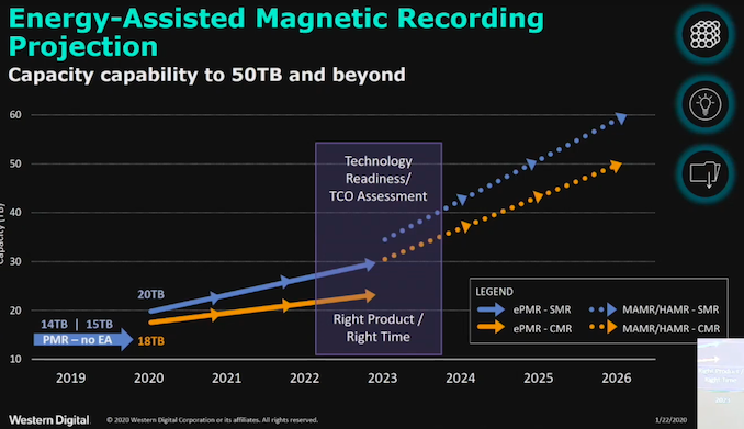
Western Digital’s development of hard drive technology is advancing on several fronts to push the limits of their high-capacity enterprise HDDs. Helium is old news, and used in all their drives larger than 10TB. Lately, the most attention has been focused on Heat Assisted Magnetic Recording (HAMR) and Microwave Assisted Magnetic Recording (MAMR), both of which fall under the heading of energy-assisted recording. Western Digital is still a few years away from deploying either HAMR or MAMR, but their upcoming generation of hard drives takes the first steps in that direction.


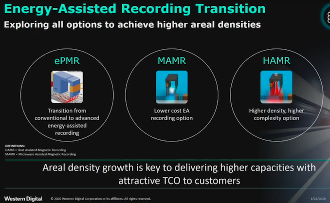
This year, WDC is starting to deliver their latest generation of high-capacity enterprise hard drives which were announced in 2019: the 16TB and 18TB Ultrastar DC HC550 and the 20TB Ultrastar DC HC640 with shingled magnetic recording (SMR). All of these new models will feature WDC’s first energy-assisted recording technology which they have dubbed ePMR. This is still a fairly ill-defined transitional feature, but it is based on some of the parts needed to implement MAMR. WDC’s roadmaps have them sticking with ePMR for a few more years before fully implementing either HAMR or MAMR technology.


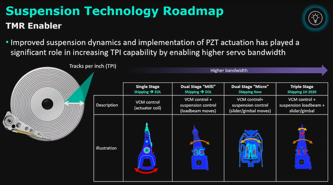
The technology to position hard drive heads has also been improving. The new generation of capacity enterprise HDDs will be Western Digital’s first to use three-stage actuators for faster and more precise seeks. Very roughly, this is akin to giving the arms elbow and write joints. This is not to be confused with multi-actuator drives that allow the heads for some platters to move independently from the heads for other platters. Seagate has been making more noise about dual-actuator hard drives and their potential to significantly improve the IOPS/TB figures that have been in decline, but Western Digital is also working on multi-actuator drives—they just haven’t shared plans for bringing them to market.


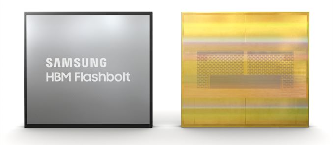
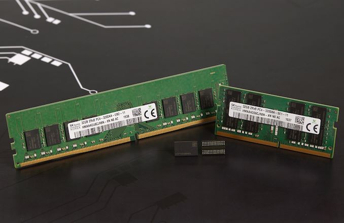
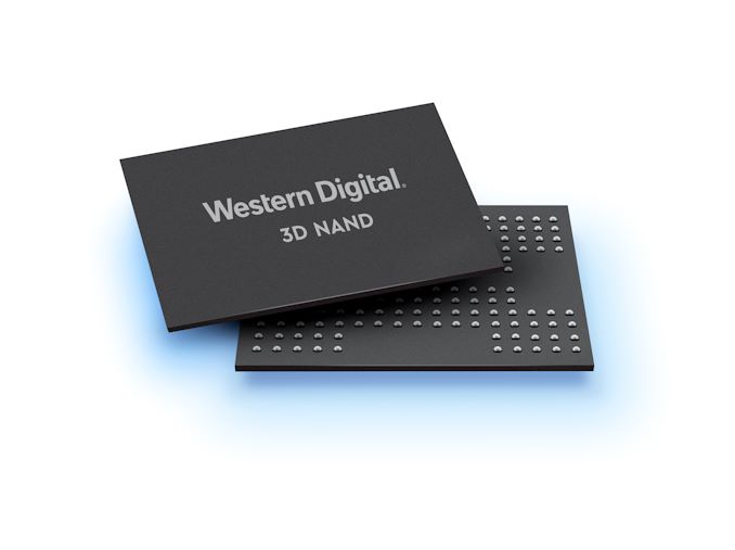
3D NAND: Price And Layer Count Rising


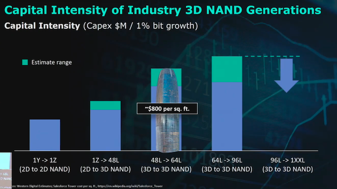
The flash memory side of Western Digital is currently focused more on delivering incremental improvements rather than introducing major technological changes. Low flash memory prices in 2018 and 2019 caused WDC and competitors to take it slow during the 64L to 96L transition, and WDC planned to make the next generation less capital-intensive after several generations of increasing transition costs.


Demand for flash memory has now caught up with supply and is expected to significant outgrow supply later this year, in part due to the CapEx cuts across most of the industry. Western Digital doesn’t expect to significantly increase their wafer output this year, but as they transition to BiCS5 that will help increase bit output somewhat. Western Digital and Kioxia have brought online their new K1 fab in Kitakami, Iwate prefecture, Japan, joining their several fabs in Yokkaichi, Mie prefecture. However, for now the extra fab capacity simply gives them the slack necessary to transition other fabs to BiCS5 and it is not yet helping increase total wafer output.


The fifth generation of Western Digital/Kioxia BiCS 3D NAND has now officially been revealed as a 112 layer design, a modest 16% increase in layer count over the 96-layer BiCS 4. The two companies have been working to also improve density in several ways other than increasing layer count, so the memory array density of BiCS5 is more like a 20% improvement over BiCS4—still not exactly revolutionary. Western Digital and Kioxia have started limited production and sampling of BiCS5 parts, but BiCS4 is still the overwhelming majority of their NAND bit production and BiCS5 won’t start ramping up seriously until the second half of 2020.


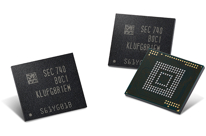
Consumer Storage: WD_BLACK for Gamers


Western Digital’s consumer strategy seems to be mostly business as usual: nothing interesting is happening with their SATA products, and their consumer NVMe drives might not see any further updates until they move to PCIe 4.0—which WD hasn’t said much about. The main exception to the stagnation is their focus on products for gamers. WDC views gamers as a more reliable and less price-sensitive customer base than consumers as a whole. Gamers are certainly one of the largest segments of consumers that still have strong growth in their local storage needs:


Western Digital now has a broad range of gamer-oriented products under their WD Black brand, which has migrated to a new look. Their SN750 NVMe SSD and all the external drives for gamers are now styled as WD_BLACK, and share many of their visual design elements.


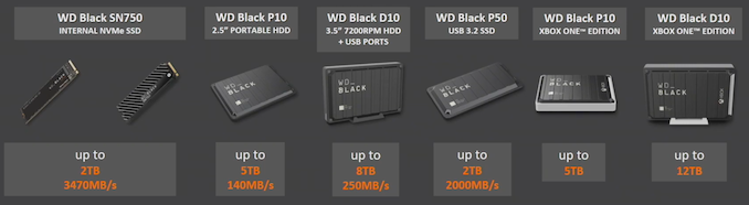
With three main families of external WD_BLACK drives plus the internal NVMe SSD and a few extra variants, the WD_BLACK brand is pretty broad. This has somewhat diluted the meaning of WD Black as referring only to the highest performance products in each category, but it means WD has plenty to offer both console and PC gamers. With a new generation of consoles arriving late this year, WD estimates the console storage market to be a multi-exabyte opportunity for 2020 alone.


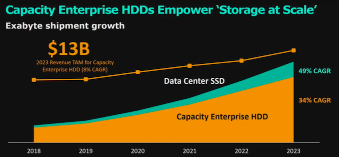
Datacenter Storage: Almost Ready for SMR to Take Off?


SSDs are an important and lucrative part of Western Digital’s datacenter and enterprise storage lineup, but in terms of bits shipped, their high-capacity hard drives are still way ahead. Both markets are still experiencing healthy growth, and the hard drives won’t be fading into irrelevance anytime soon.


Western Digital’s hard drive R&D is focused almost exclusively on serving their enterprise and datacenter customers. The flash memory business isn’t quite so narrowly focused, but the server market is definitely where Western Digital would prefer to be selling most of their NAND.


Currently, Western Digital’s market share for enterprise SSDs is just under 10%, and their ability to expand was a bit limited during the last quarter due to supply chain issues with components other than their NAND flash. With that issue now out of the way, WDC hopes to double their market share over the next year, with a target of 20%. They have scored several new design wins recently for their enterprise NVMe drives, and one of their new customers is a major hyperscale cloud service provider. Even if they fall short of their market share target, they’ll be making a lot more money in this segment over the next year as prices rise.


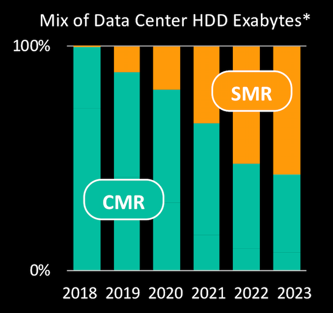
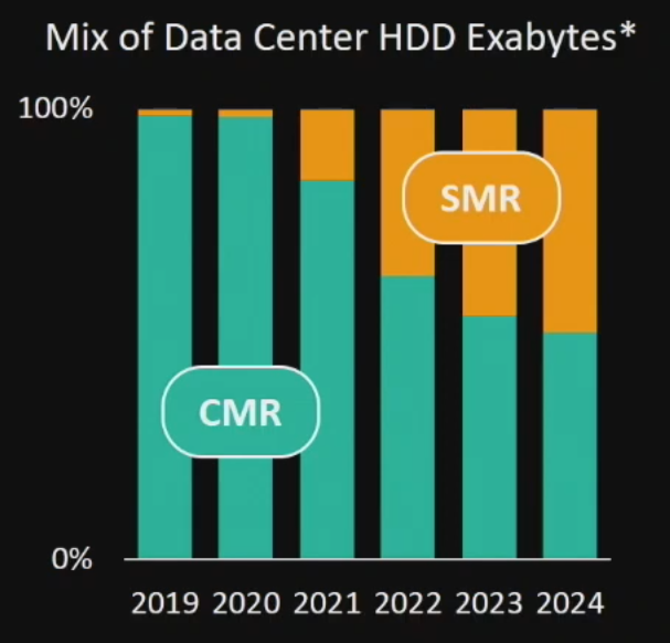
Left: April 2019 projections Right: January 2020 projections


SMR hard drives have been available for years, but have not yet seen mass adoption in the datacenter. The performance downsides of SMR are significant, and when SMR only makes the difference between 18TB and 20TB, it’s a tough sell. As recently as last spring, Western Digital was projecting that SMR hard drives would make up a non-trivial fraction of datacenter hard drive exabytes shipped starting in 2019, with growth toward ~50% market hare by around 2023. Now Western Digital’s updated projections acknowledge that SMR went basically nowhere in 2019 an will do the same for 2020, but they are adamant that it will begin to take off in 2021. Several things need to change about the current situation before that can happen.


First, SMR hard drives need to have compelling advantages. Western Digital promises that the capacity gap between CMR and SMR drives will widen in the coming years, though they stop short of promising that SMR will have a significant advantage in $/TB. Even at comparable $/TB, larger drives can provide a lower TCO for large deployments by reducing the number of servers needed to hit a certain capacity point. This is an argument Western Digital has been making to push their larger CMR drives as well:


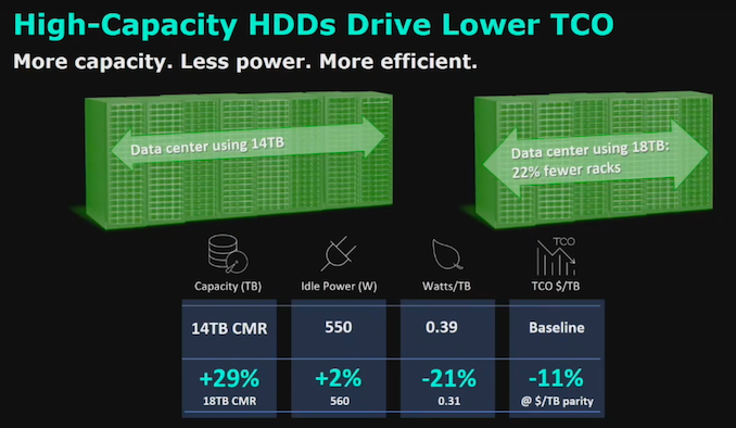
WDC’s estimates for how their 18TB HDDs can offer lower TCO than 14TB at the same $/TB


The other big change necessary for SMR to succeed is that the performance penalties need to become more manageable. SMR drives are fundamentally unable to support random writes. They need to buffer and write an entire track at a time, and tracks that overlap can only be rewritten in-order. Drive-Managed SMR HDDs let the host system pretend those restrictions don’t exist by using large write caches. Western Digital believes the best way to get good performance out of SMR drives is to instead do Host-Managed SMR where software is aware of the restrictions on writes within a shingled zone. This obviously requires major changes to the software stack, and according to WDC this is what’s been holding back adoption of SMR in the datacenter. Western Digital has been putting in a lot of work to help prepare the software ecosystem for SMR hard drives, and they believe that by 2021 they will have major customers will be ready to roll out SMR-aware software as part of a mass deployment of SMR drives.


Zoned Storage Initiative


The data access pattern restrictions imposed by SMR hard drives are eerily similar to some of the fundamental challenges of working with NAND flash memory’s small page vs huge erase block structure. For the past year, Western Digital has been promoting their Zoned Storage Initiative that seeks to address both of these challenges at once and allow applications to deal generically with zoned storage devices, be they SSDs or SMR HDDs. The ATA and SCSI command sets already have extensions for host-managed SMR. WDC has been helping NVMe develop the Zoned Namespace (ZNS) extension to provide a similar interface to SSDs.


For hard drives the benefits of SMR are small but due to get bigger. For SSDs, switching to a zoned model can allow for drastically smaller overprovisioning ratios and onboard DRAM, so drives can be cheaper while offering similar performance on many workloads. Properly host-managed IO can also significantly reduce write amplification, allowing for higher effective write endurance.


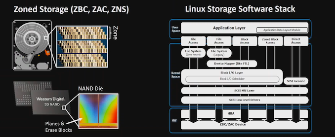
Western Digital is already shipping the Ultrastar SN340 NVMe SSD that provides some of those advantages without using the upcoming ZNS extension, by having the Flash Translation Layer work with 32kB blocks rather than 4kB. Like a drive-managed SMR HDD, this means the SN340 will allow the host to issue random write commands, but performance for those will suck. Thus, the SN340 is targeted only at the most read-intensive workloads. A ZNS SSD would more likely deal with zone sizes on the order of tens of megabytes rather than 32kB, and would require the host system to ensure its writes are sequential within each zone to avoid the horrible random write performance.


The NVMe Zoned Namespace extension is likely to be ratified this year. Western Digital’s software work in this space has been all open-source, focusing on support in the Linux kernel and developing the necessary tools and libraries for a zoned storage ecosystem.


Source: AnandTech – Western Digital Roadmap Updates: Energy Assisted Recording, Multi-Stage Actuators, Zoned Storage

Faster, Cheaper, Power Efficient UFS Storage: UFS 3.1 Spec Published

JEDEC has published its UFS 3.1 specification (aka JESD220E), which adds several performance, power, cost-cutting, and reliability-related features to the standard. The new capabilities promise to increase real-world device performance, minimize power usage, potentially cut costs of high-capacity storage devices, and improve the user experience.


Devices compliant with the UFS 3.1 standard continue to use MIPI’s M-PHY 4.1 physical layer with 8b/10b line encoding, MIPI’s UniPro 1.8 protocol-based interconnect layer (IL), and support HS-G4 (11.6 Gbps) per lane data rates. Meanwhile, the new version of the specification supports three new features: Write Booster, Deep Sleep, and Performance Throttling Notification. In addition, JEDEC published a specification for Host Performance Booster technology. All of these features are already supported by modern SSDs, so the UFS 3.1 spec and HP bring UFS storage devices closer to SSDs in terms of functionality.


As the name suggests, Write Booster is designed to increase write speeds by using a pseudo-SLC cache. A similar technology is already used with SSDs and various miniature NVMe-powered storage devices, such as those used in Apple’s iPhone/iPad. Also, caching is supported by the SD 6.0 standard to hit write performance targets.


The second important new capability of the UFS 3.1 technology is Deep Sleep, a new lower power state designed for cheap UFS devices that use the same voltage regulators for storage and other functions.


Yet another new capability is Performance Throttling Notification that enables the UFS device to inform the host about performance throttling when overheating. Ultimately, avoiding throttling means a more consistent performance.


Last but not least is Host Performance Booster, which caches the logical-to-physical (LTP) address map of a UFS device in the system’s DRAM to improve performance. Mobile applications use a lot of random read operations and therefore access LTP address maps often. Meanwhile, because storage capacity of UFS devices is growing, so is LTP size, which makes it harder (and more expensive) to keep it in a controller’s memory. By hosting LTP in fast system DRAM and delivering an LTP hint when sending an I/O request, it is possible to improve random read performance and reduce the cost of the UFS controller. Samsung worked on HPB feature several years ago and claims that it can improve random read performance by up to 67%. In SSDs, HMB capability is used to cut down costs, so HPB will prevent UFS devices from getting too expensive as their capacity increases. It is important to note though that HPB is not a mandatory, but an optional feature for now.


To sum things up, while UFS 3.1-compliant storage devices will continue to offer a theoretical maximum bandwidth of up to 23.2 Gbps (2.9 GB/s) when HS-G4 is used (given the encoding used by M-PHY 4.1, actual achievable bandwidth should be something like 1.875 GB/s). However, with Write Booster and HPB implemented, real-world performance of upcoming UFS drives will get higher and more consistent. Meanwhile, Deep Sleep will help to prolong battery life of lower cost devices.


Related Reading:


Source: JEDEC


Source: AnandTech – Faster, Cheaper, Power Efficient UFS Storage: UFS 3.1 Spec Published

Western Digital and Kioxia Announce BiCS5 112-Layer 3D NAND

Western Digital and Kioxia have announced the successful development of their newest generation of 3D NAND flash memory. Their fifth-generation BiCS 3D NAND has commenced production in the form of a 512 Gbit TLC part, but will not ramp up to “meaningful commercial volumes” until the second half of the year. Other parts planned for this generation include 1Tbit TLC and 1.33 Tbit QLC dies.


The BiCS5 design uses 112 layers compared to 96 for BiCS4. BiCS5 is the second generation from WDC/Kioxia to be constructed with string stacking, and is probably built as two stacks of about 56 active layers each. Even though 112 layers is only a ~16% increase over the previous generation, the companies are claiming a density increase of up to 40% (comparing 112L 512Gb TLC against 96L 256Gb TLC, by bits per wafer), thanks to other tweaks to the design that allow for shrinking horizontal dimensions. The density of the memory array itself is said to be about 20% higher. The memory interface speed has been increased by 50%, which should put it at 1.2GT/s, on par with most of the 96L competitors.


BiCS5 parts will begin sampling this quarter. With production ramping up in the second half of the year, SSDs and other products using BICS5 will likely hit the market around the end of 2020 at the earliest. Western Digital has previously stated that they intended for the BiCS5 transition to require lower CapEx than the 64L to 96L transition, reversing the trend of steadily more expensive generational updates. This means that the migration to 112L will probably be even slower than the last transition, and 96L BiCS4 will be a major part of their production volume for quite a while.


Source: AnandTech – Western Digital and Kioxia Announce BiCS5 112-Layer 3D NAND

ASRock’s X570D4I-2T: A Mini-ITX AMD X570 Motherboard with Intel’s 10 GbE Controller

ASRock Rack has revealed a rather interesting Mini-ITX motherboard for AMD’s Ryzen 2000 and 3000-series processors with Intel’s X550 10 GbE controller. The X570D4I-2T platform can be used both for high-performance desktops and for small form-factor servers/NAS with robust storage capabilities.


The ASRock Rack X570D4I-2T motherboard is based on AMD’s X570 chipset and supports all the latest AMD Ryzen 2000/3000-series processors with up to 16 cores and a 105 W TDP. The platform has four DDR4 SO-DIMM slots supporting up to 64 GB of DDR4-2400 memory with or without ECC, one PCIe 4.0 x4 slot for graphics cards (when used with an appropriate CPU), one M.2-2280 slot supporting PCIe 4.0 x4 or SATA SSDs, and two OCulink connectors that bring support for eight SATA 6 Gbps ports (controlled by the X570). Since the Mini-ITX motherboard can be used for servers, it also carries the ASpeed AST2500 BMC.


On the I/O side of matters, the ASRock Rack X570D4I-2T has two 10 GbE ports (controlled by the Intel X550-AT2), a GbE port for remote management, two USB 3.1 Gen 1/2 (depends on redriver) Type-A connectors, one USB 3.1 Gen 1 header for front panels, and a D-Sub display output.


The choice of the 10 GbE controllers may seem a bit odd since we are talking about an AMD-based motherboard, but it looks like ASRock Rack originally developed the X570D4I-2T for a particular customer that required an Intel NIC, but wanted to take advantage of AMD’s latest desktop platform. In fact, the latter does have a unique set of features not available elsewhere: a support for a 16-core (reasonably priced) CPU, eight SATA ports, and 20 PCIe 4.0 lanes. Using the X570D4I-2T, it is possible to build an extremely advanced desktop PC with discrete graphics card and vast storage capabilities, or a small form-factor server/NAS featuring 128 TB of SATA storage and terabytes of ultra-fast NVMe storage that can be accessed using 10 GbE ports.


Brief Specifications of ASRock’s X570D4I-2T
  X570D4I-2T
CPU AMD Ryzen 2000 and 3000-series CPUs with up to 105 W TDP
PCH AMD X570
BMC ASpeed AST2500
Memory  4 × SO-DIMM slots, up to 64 GB of DDR4-2400
Storage M.2 1 × M.2-2280 SSD with SATA or PCIe 4.0 x4 interface
SATA 8 × SATA HDDs or SSDs
Wi-Fi
WWAN
Ethernet 2 × 10 GbE connectors (Intel X550-AT2)

1 × GbE (Realtek RTL8211E)
Display Outputs 1 × D-Sub
Audio
USB Internal 1 × USB 3.0
External 2 × USB 3.1 Gen 1/2 Type-A
Additional I/O
Power 8-pin (DC-IN) + 4-pin (ATX) + 4-pin (HDD PWR)
Temperatures Operating 10°C ~ 35°C
Storing -40ºC – 70°C
OS Windows, Linux

Compatible with other operating systems

The ASRock Rack X570D4I-2T motherboard is now listed at the company’s website, so expect it to be available shortly. Considering all the peculiarities of the platform, it is hard to tell whether this one will be available widely in retail (if at all), but at least it can be ordered directly from the company.


Related Reading:


Source: ASRock Rack (via Hermitage Akihabara)


Source: AnandTech – ASRock’s X570D4I-2T: A Mini-ITX AMD X570 Motherboard with Intel’s 10 GbE Controller

EKWB Releases New Closed-Loop EK-AIO Cooling Systems w/RGB

Historically, EKWB has been best known for its custom, open-loop liquid cooling systems designed for experienced enthusiasts. But as closed-loop factory-assembled cooling systems are increasingly popular among many DIYers, EKWB has also previously branched out into its modular EK-MLC Phoenix coolers, which combine ease-of-assembly and ability to customize them. Now, to cater to even more mainstream audience that tends to use prêt-à-porter coolers, EKWB is unveiling a new lineup of all-in-one coolers, the EK-AIO family.


EKWB’s EK-AIO lineup of liquid coolers that require no assembly or maintenance consists of three models: the EK-AIO 120 D-RGB, EK-AIO 240 D-RGB, and EK-AIO 360 D-RGB. The cooling systems use a water block featuring an SPC- style pump as well as a copper cold plate. As the names of the coolers suggest, the devices come with either a 120-mm radiator with one EK Vardar fan, a 240-mm radiator with two fans, or as a 360-mm radiator with three fans. The radiators have 12 channels to maximize cooling efficiency and are 28 mm thick to be compatible with the vast majority of modern PC cases.


In line with modern trends, EKWB’s EK-AIO family of coolers are lit with addressable RGB LEDs that can be controlled using software from leading motherboards makers. The LEDs are located inside the water block and under the motor hub of fans creating rather interesting effects.


As far as compatibility is concerned, EKWB’s EK-AIO come with mounting kits supporting modern AMD’s AM4 and similar sockets (so, no sTR4) and Intel’s LGA1155 as well as LGA2066.


EKWB’s closed-loop EK-AIO 120 D-RGB, EK-AIO 240 D-RGB, and EK-AIO 360 D-RGB coolers will be available starting February 28. The cheapest model with a 120-mm radiator is priced at €74.9, the mid-range SKU costs €124.9, whereas the highest-end flavor with a 360-mm radiator and three fans carries an MSRP of €149.9. All units are covered with a five-year warranty.


Specifications of EKWB’s EK-AIO D-RGB Cooling Systems
  General Specifications
Fan (single) Speed (RPM) 600 – 2,500 ± 10% RPM
Airflow (CFM) up to 89 CFM
Static Pressure (mm-H2O) up to 4.3 mm-H2O
Noise (dBA) up to 38.4
Power ? W
MTBF (hrs) ? @ unknown oC
Connector 4-pin PWM connector
Pump Speed (RPM) 450 – 2,600 ± 300 RPM
Life Expectancy ? @ unknown oC
Power ? W
Tubing Length 300 mm
Compatibility AMD AM4, AM3+, AM3, AM2, FM2+, FM2, FM2+, FM1
Intel LGA 1151, 1150, 1155, 1156, 1366, 2011, 2011-3, 2066
TDP various

Related Reading:


Source: EKWB


Source: AnandTech – EKWB Releases New Closed-Loop EK-AIO Cooling Systems w/RGB

EnGenius Reveals ‘Affordable’ Multi-Gig Switches with PoE: 8 2.5GBASE-T and 4 10GbE SFP+ Ports

EnGenius has unveiled a new series multi-gigabit PoE++ L2+ networking switches with multiple NBASE-T ports. The EnGenius ECS2512FP and ECS2512 switches are designed for small and medium businesses as well as large living environments, and along with their fast switching capabiltiies, one of the models is also capable of Power over Ethernet to deliver power to remote, high-performance devices like Wi-Fi 6 access points. Both models can be managed remotely using EnGenius cloud-based software. The manufacturer is calling its new switches ‘affordable’, though without listing official prices.


Both new switches from EnGenius — the ECS2512FP and the ECS2512 — support 120 Gbps of switching capacity and are fed via eight 2.5GBASE-T ports along with four 10GbE SFP+ slots for fiber uplinks. Meanwhile, the more advanced ECS2512FP model supports the IEEE 802.3bt Power-over-Ethernet, allowing it to transfer up to 240 W of power to such power-hungry devices as Wi-Fi 6 access points, PTZ cameras, or AV controllers. 


One of the key features of the latest EnGenius switches is their support for the company’s subscription-free EnGenius Cloud that allows to monitor system metrics in real time, display network topology, troubleshoot, problems, and analyze network’s behavior. According to the company, its switches and cloud services provide ‘enterprise-class features’ and essentially simplify monitoring of networks. While such capabilities bring a lot of value for companies, they come at a cost that typically makes these kinds of multi-gig switches prohibitively expensive for consumers.


EnGenius says that its ECS2512FP and ECS2512 switches will hit the market next month and that they will be ‘affordable’. Unfortunately, without an actual price it is impossible to say whether the switches will be reasonably priced for an average person, or for a business that wants to save on multi-gig network management.


Related Reading:


Source: EnGenius


Source: AnandTech – EnGenius Reveals ‘Affordable’ Multi-Gig Switches with PoE: 8 2.5GBASE-T and 4 10GbE SFP+ Ports