OWC Refreshes Mercury Elite Pro DAS: Up to 16 TB over USB 3.2

OWC has announced a new version of its Mercury Elite Pro DAS, the company’s entry-level external storage box. The refreshed DAS can house one 3.5-inch hard drive, allowing it to provide capacities of up to 16 TB using today’s HDDs.


The OWC Mercury Elite Pro DAS is available in 1 TB, 2 TB, 4 TB, 6 TB, 8 TB, 12 TB, 14 TB, and 16 TB versions. The devices can be stacked, so those who need greater capacities can easily get it. All the SKUs are powered by 7200 RPM hard drives, so they offer a rather decent level of performance, up to 283 MB/s, which is good enough for music, videos, photos, and business files. Externally, the DAS has a USB 3.2 Gen 1 interface with up to 5 Gbps throughput.


The Mercury Elite Pro DAS comes in a brushed aluminum chassis with venting, so it does not rely on active cooling, making the hard drive inside the only major noise source.


OWC’s new entry-level DAS is compatible with Apple macOS X, Microsoft Windows, Linux, Sony PlayStation 4, Xbox consoles, and Smart TVs. In addition, they are support Apple Time Machine and Windows File History backups.


OWC has already started sales of the Mercury Elite Pro. Just the enclosure itself is priced at $49, a 2 TB SKU costs $129, whereas the top-of-the-range 16 GB module carries a $579 price tag.


Related Reading:


Source: OWC


Source: AnandTech – OWC Refreshes Mercury Elite Pro DAS: Up to 16 TB over USB 3.2

The GIGABYTE MZ31-AR0 Motherboard Review: EPYC with Dual 10G

The workstation and server markets are big business for not only chip manufacturers such as Intel and AMD, but for motherboard vendors too. Since AMD’s introduction of its Zen-based EPYC processors, its prosumer market share has been slowly, but surely, creeping back. One example of a single socket solution available on the market is the GIGABYTE MZ31-AR0. With support for AMD’s EPYC family of processors, the MZ31-AR0 has some interesting components including its 2 x SFP+ 10 G Ethernet ports powered by a Broadcom BCM57810S controller, and four SlimSAS slots offering up to sixteen SATA ports. 


Source: AnandTech – The GIGABYTE MZ31-AR0 Motherboard Review: EPYC with Dual 10G

Intel’s new ‘Single Customer’ Ice Lake Mobile CPUs: Are These in the Macbook Air?

It was recently brought to our attention that three new Ice Lake CPUs were listed on Intel’s online ARK database of products: the Core i7-1060NG7, the Core i5-1030NG7, and the Core i3-1000NG4. These differ from the ‘consumer’ released products by having an ‘N’ in them, and specification-wise these CPUs have a slightly higher TDP along with a slightly higher base clock, as well as being in a smaller package. We reached out to Intel, but in the meantime we also noticed that the CPUs line up perfectly with what Apple is providing in its latest Macbook Air.


Intel’s Ice Lake family is the first generation of 10nm processors that the company has made widely available. We’ve covered Intel’s ups and downs with the 10nm process, and last year it launched Ice Lake as part of its 10th Generation Core family, focusing more on premium products that need graphics horsepower or AI acceleration. In the initial announcement, Intel stated that there would be nine different Ice Lake processors coming to market, however we learned that the lower-power parts would take longer to arrive.


These three new CPUs actually fall under that ‘lower power’ bracket, meaning they were meant to be coming out about this time, but are labelled differently to the processors initially announced. This is because these new CPUs are officially listed as ‘off-roadmap’, which is code for ‘not available to everyone’. Some OEMs, particularly the big ones like Apple, or sometimes HP and others, will make a request to Intel to develop a special version of their products just for them. This product is usually the same silicon as before, but binned differently, often to tighter constraints: it might differ in frequency, TDP, core count, or the way it is packaged. This more often happens in the server space, but can happen for notebooks as well, assuming you can order a larger amount.


Intel Ice Lake-Y Variants
AnandTech 1060N

G7
1060

G7
  1030N

G7
1030

G7
  1000N

G4
1000

G4
Cores / Threads 4 / 8 4 / 8   4 / 8 4 / 8   2 / 4 2 / 4
L3 Cache 8 MB 8 MB   6 MB 6 MB   4 MB 4 MB
Base Freq (GHz) 1.20 1.00   1.10 0.80   1.10 1.10
Turbo Freq (GHz) 3.80 3.80   3.50 3.50   3.20 3.20
TDP 10 W 9 W   10 W 9 W   9 W 9 W
LPDDR4X 3733 3733   3733 3733   3733 3733
GPU EUs 64 64   64 64   48 48
GPU Freq (MHz) 1100 1100   1050 1050   900 900
Package T5 T4   T5 T4   T5 T4

These new CPUs are different because they have an ‘N’ in the name. This translates, in the case of the Core i7, to +1W on the TDP, +200 MHz on the base frequency, and a much smaller package size. They are all classified as Iris Plus graphics, and the G7 indicates 64 EUs while the G4 indicates 48 EUs. Interestingly the new CPUs have Intel’s TXT and Optane Memory Support disabled. Increasing the TDP by 11% and the base frequency by 20% is probably very reasonable – ultimately the TDP affects more for the sustained performance, for which customers that want custom versions are probably optimizing for quite well.


Another aspect is the smaller package size. Intel for the Ice CPUs traditionally has two packages – a Type 3 at 50x25mm, and a Type 4 at 26.5 x 18.5 mm. With Type 4, the CPU and IO chips are close together and have a shim to stiffen the package. This new package seems to be off-roadmap as well, without the shim – a ‘Type 5’ package if you will. The smaller package also helps in designing the system, leaving more room for other components. Arguably this is the biggest change with these CPUs, reducing the package from 26.5 mm by 18.5 mm to 22.0 mm by 16.5 mm, a 26% size reduction.


We suspect these are the CPUs in the most recent updates to Apple’s Macbook Air line. Apple historically does not list exactly which processors it uses in its devices, but the website shows the following:


These specifications line up. Two of the three CPUs already have Geekbench benchmark results submitted to the online database.


When we approached Intel asking what these CPUs were, and the official line is:


“The ‘N’ notes a slightly differentiated, customer-specific version of those SKUs. Those slight differences require a signifier for our internal SKU management and ordering systems. The N is not a new subfamily or directly connected to a specific set of features, for example.”


This goes in line with what we stated above about customer-specific binning. Apple will no doubt be ordering a few million of these CPUs, so Intel is prepared to add an extra binning step just for the business.


Related Reading


Source: AnandTech – Intel’s new ‘Single Customer’ Ice Lake Mobile CPUs: Are These in the Macbook Air?

Samsung to Produce DDR5 in 2021 (with EUV)

Samsung is on track to start volume production of DDR5 and LPDDR5 memory next year using a manufacturing technology that will take advantage of extreme ultraviolet lithography (EUVL). In fact, Samsung has been playing with EUV-enabled DRAM fabrication process for a while and has already validated DDR4 memory with select partners.


To date, Samsung has produced and shipped a million of DDR4 DRAM modules based on chips made using the company’s D1x process technology that uses EUV lithography. These modules have completed customer evaluations, which proves that Samsung’s 1st Generation EUV DRAM technology enables to build fine circuits. Samsung’s D1x is an experimental EUVL fabrication process that was used to make experimental DDR4 DRAMs, though it will not be used any further, the company said.


Instead, to produce DDR5 and LPDDR5 next year, the company will use its D1a, a highly-advanced 14 nm-class process with EUV layers. This technology is expected to double per-wafer productivity (DRAM bit output) when compared to D1x technology, which indicates that it uses thinner geomtries. Samsung did not reveal whether its D1a also uses other innovations (in addition to EUVL), such as pillar cell capacitors and dual work function layers for buried wordline gates, as anticipated by analysts from TechInsights who believe that scaling DRAM cell transistors and capacitor structures offer limited capability to scale further from current levels.


Timeline of Samsung DRAM Milestones
Date Milestone
2021 4th-gen 10nm-class (1a) EUV-based

16Gb DDR5/LPDDR5 mass production
March 2020 4th-gen 10nm-class (1a) EUV-based DRAM development
September 2019 3rd-gen 10nm-class (1z) 8Gb DDR4 mass production
June 2019 2nd-gen 10nm-class (1y) 12Gb LPDDR5 mass production
March 2019 3rd-gen 10nm-class (1z) 8Gb DDR4 development
November 2017 2nd-gen 10nm-class (1y) 8Gb DDR4 mass production
September 2016 1st-gen 10nm-class (1x) 16Gb LPDDR4/4X mass production
February 2016 1st-gen 10nm-class (1x) 8Gb DDR4 mass production
October 2015 20nm (2z) 12Gb LPDDR4 mass production
December 2014 20nm (2z) 8Gb GDDR5 mass production
December 2014 20nm (2z) 8Gb LPDDR4 mass production
October 2014 20nm (2z) 8Gb DDR4 mass production
February 2014 20nm (2z) 4Gb DDR3 mass production
February 2014 20nm-class (2y) 8Gb LPDDR4 mass production
November 2013 20nm-class (2y) 6Gb LPDDR3 mass production
November 2012 20nm-class (2y) 4Gb DDR3 mass production
September 2011 20nm-class (2x) 2Gb DDR3 mass production
July 2010 30nm-class 2Gb DDR3 mass production
February 2010 40nm-class 4Gb DDR3 mass production
July 2009 40nm-class 2Gb DDR3 mass production

Usage of EUVL will enable Samsung (and eventually other memory makers) to reduce (or eliminate) usage of multi patterning, which enhances patterning accuracy and therefore improves performance and yields. The latter will be beneficiary for production of high-performance high-capacity DDR5 chips as they are meant to increase both performance (up to DDR4-6400) and capacity (up to 32 Gbps). Samsung has not officially revealed how many EUV layers do its D1x and D1a process technologies use.


In addition to revealing its EUV-related achievements, Samsung also said that in the second half this year its P2 fab near Pyeongtaek, South Korea, will begin operations later this year. Initially, the facility will ‘make next-generation premium DRAMs’.


Jung-bae Lee, executive vice president of DRAM Product & Technology at Samsung Electronics, said the following:


“With the production of our new EUV-based DRAM, we are demonstrating our full commitment toward providing revolutionary DRAM solutions in support of our global IT customers. This major advancement underscores how we will continue contributing to global IT innovation through timely development of leading-edge process technologies and next-generation memory products for the premium memory market.”


Related Reading:


Source: Samsung


Source: AnandTech – Samsung to Produce DDR5 in 2021 (with EUV)

Samsung Reveals All-in-One Power Management ICs for Wireless Earbuds

Samsung has formally announced two new all-in-one power management integrated circuits (PMIC) developed specifically for “True Wireless Stereo” (TWS) devices (a.k.a. earbuds). The highly integrated PMICs are being touted as allowing earbuds to be built with longer battery lives and better ergonomics. And because this is Samsung, the the first earbuds to use the new PMICs are fittingly Samsung’s own Galaxy Buds+.


Samsung’s family of PMICs for TWS devices includes the MUA01 designed for charging cases, as well as the MUB01 for the earbuds themselves. Previously, power management solutions for earbuds have used 5 to 10 discrete components (see the image below), including switching chargers and discharge circuits, which take precious space. Samsung says that it has managed to integrate all of these components into one chip, occupying half the space as before, which enables it to save space inside earbuds and charging cases. Ultimately, the goal is to free up space in earbuds to integrate higher-capacity batteries, better speakers, and refine ergonomics.


The MUA01 supports both wired as well as wireless charging (and happens to be the industry’s first solution of this kind to support both) and is compatible with the latest Wireless Power Consortium’s Qi 1.2.4 specification. Like other devices of this kind, the MUA01 integrates a microcontroller unit (MCU) with eFlash to enable firmware upgrades. Furthermore, both MUA01 and MUB01 support power line communication (PLC) technology that enables earpices and charging cases to share essential information, such as battery levels.


Samsung has already started to mass produce its MUA01 and MUB01 PMICs and uses them inside its recently announced Galaxy Buds+ that are rated for up to 11 hours of operation on one charge.


Related Reading:


Source: Samsung


Source: AnandTech – Samsung Reveals All-in-One Power Management ICs for Wireless Earbuds

GOODRAM Announces Entry-Level PX500 SSDs: Bringing NVMe to Budget Drives

As more SSD manufacturers introduce their inexpensive NVMe PCIe drives, the market of entry-level SSDs is slowly but surely moving away from SATA altogether. Case in point this week is GOODRAM, yet another SSD manufacturer who is launching a family of entry-level NVMe SSDs that are priced to compete with their SATA counterparts. 


GOODRAM’s PX500-series SSDs are based on Silicon Motion’s SM2263XT controller and come with 256 GB, 512 GB, or 1 TB of usable 3D TLC NAND memory. The entry-level drives fully support modern SSD features like the NVMe 1.3a protocol, end-to-end data protection, L1.2 low power mode, and AES-256 encryption. What’s also notable is that the manufacturer is specifically designing the M.2 2280 form-factor drives with laptop compatibility in mind; so rather than using a large metal heatsink, the drives are covered by a thin heat spreader made of plastic-like material so that they fit into the tight spaces afforded by laptops.


When it comes to performance, GOODRAM rates the new PX500-series SSDs for up to 2050 MB/s sequential read speeds, up to 1650 MB/s sequential write speeds, and up to 240,000/280,000 random read/write IOPS, which is in line with the capabilities of the controller and performance levels offered by competing drives.


General Specifications of GOODRAM’s PX500 SSDs
Capacity 256 GB 512 GB 1 TB
Model Number SSDPR-PX500-256-80 SSDPR-PX500-512-80 SSDPR-PX500-01T-80
Controller Silicon Motion SM2263XT
NAND Flash 3D TLC NAND
Form-Factor, Interface M.2-2280, PCIe 3.0 x4, NVMe 1.3a
Sequential Read 1850 MB/s 2000 MB/s 2050 MB/s
Sequential Write 950 MB/s 1600 MB/s 1650 MB/s
Random Read IOPS ~102K IOPS ~173K IOPS ~240K IOPS
Random Write IOPS ~230K IOPS ~140K IOPS ~280K IOPS
Pseudo-SLC Caching Supported
DRAM Buffer No
TCG Opal Encryption No
Power Management L1.2 power mode support for ultra-low power consumption

Idle: ? W

Active: ? W
Warranty 3  years
MTBF 1,500,000 hours (?)
TBW ? ? ?
Additional Information Link
Launch Price ? ? ?

Wilk Electronik SA, the owner of the GOODRAM brand, has not announced official MSRPs for its PX500 SSDs, but the general principle here is that they are supposed to launch at prices that are close to those for M.2 SATA SSDs.


Related Reading:


Source: GOODRAM


Source: AnandTech – GOODRAM Announces Entry-Level PX500 SSDs: Bringing NVMe to Budget Drives

IBM & Partners to Fight COVID-19 with Supercomputers, Forms COVID-19 HPC Consortium

The SARS-CoV-2 coronavirus and the outbreak of the COVID-19 pandemic has disrupted multiple business events as well as high-tech product launches in the recent months and has all the chances to disrupt the world’s economy quite drastically. So in a bid to better better understand the disease and develop treatments as well as potential cures, IBM this week established the COVID-19 High Performance Computing Consortium, which will be enlisting the United States’ various public and private supercomputers and compute clusters to run research projects related to the disease.


Together with IBM, the White House Office of Science and Technology Policy and the U.S. Department of Energy and others, the COVID-19 High Performance Computing Consortium pools together 16 supercomputers with that together offer a total of over 330 PetaFLOPS of compute power, a combination of 775,000 CPU cores as well as 34,000 GPUs. The systems will be used to run research simulations in epidemiology, bioinformatics, and molecular modeling. All of these virtual experiments are meant to greatly speed up research of the COVID-19 disease as well as possible treatments. Eventually, the knowledge obtained during this work could allow to develop vaccines and other treatments against the SARS-CoV-2 coronavirus itself. Meanwhile, the COVID-19 HPC Consortium will first prioritize projects that can have ‘the most immediate impact’. Researchers are advised to submit their proposals to the consortium via a special online portal.


So far, IBM’s Summit supercomputer at the Oak Ridge National Laboratory has enabled researchers from ORNL and the University of Tennessee to screen 8,000 compounds to discover those that are most likely to bind to the main “spike” protein of the coronavirus, and thus prevent it from infecting host cells. To date, scientists recommended 77 promising small-molecule mixtures that could now be evaluated experimentally.


The pool of supercomputers participating in IBM’s COVID-19 HPC Consortium currently includes machines operated by IBM, Lawrence Livermore National Lab (LLNL), Argonne National Lab (ANL), Oak Ridge National Laboratory (ORNL), Sandia National Laboratory (SNL), Los Alamos National Laboratory (LANL), the National Science Foundation (NSF), NASA, the Massachusetts Institute of Technology (MIT), Rensselaer Polytechnic Institute (RPI), and other technology companies (including Amazon, Google, Cloud, and Microsoft).


Related Reading:


Sources: IBM, COVID-19 High Performance Computing Consortium


Source: AnandTech – IBM & Partners to Fight COVID-19 with Supercomputers, Forms COVID-19 HPC Consortium

Computex 2020 Moved to September In Response to Coronavirus Pandemic

Over the past month and a half, we’ve written about several technology industry trade shows that had been radically transformed, virtualized, or outright canceled due to the ongoing SARS-CoV-2 coronavirus pandemic. And now the epidemic has put the brakes on one of the largest tradeshows yet, with Computex organizer TAITRA officially postponing the show to late September.


As one of the biggest IT trade shows in the world, and easily the largest show for PC products period, Computex is a major event for the industry as a whole. The Taiwanese show brings together local vendors from Taiwan, foreign vendors from China, the United States, and beyond, as well as press and buyers from all over. The 2020 show in particular was expected to be a big draw on the PC side of matters, as both AMD and Intel were relatively quiet at CES 2020, instead gearing up to deliver their next generation of products later this year.


Unfortunately, despite their best efforts to keep the show on schedule, TAITRA has finally had to bow to the worsening coronavirus situation, and abort their plans to host the show in early June as previously scheduled. Interestingly, the group is not canceling the show outright, and instead has rescheduled it to September 28th through the 30th. To date, very few events have successfully been rescheduled to later dates, but then TAITRA is the first to try to move an event to the fall, and citing analyst reports, believes that the coronavirus situation will be under control before the rescheduled show is set to take place.


Overall, this marks the second time that Computex has been disrupted due to a coronavirus outbreak. The show was famously delayed in 2003, when the original SARS virus resulted in the show being rescheduled to a similar late-September showing. And although it was significantly reduced in size, the rescheduled show was none the less a small success. So here’s to hoping we’ll be reporting the same thing later this year in September of 2020.


Source: AnandTech – Computex 2020 Moved to September In Response to Coronavirus Pandemic

BenQ Unveils SW321C: A 32-Inch Pro Monitor with Wide Color Gamuts & USB-C

BenQ has introduced a new 32-inch professional-grade display designed for photographers and post-production specialists. Dubbed the SW321C, the monitor is for professionals who need wide color spaces like the Adobe RGB and the DCI-P3, as well as HDR transport support. And, like many other contemporary displays, BenQ’s new LCD is equipped with a USB Type-C input.


Under the hood, the BenQ AQColor SW321C uses a 10-bit 32-inch IPS panel featuring a 3840×2160 resolution, a 250 nits typical brightness, a 1000:1 contrast ratio, a 5 ms GtG response time, a 60 Hz refresh rate, and 178° viewing angles. The monitor uses a LED backlighting that is tailored to ensure brightness uniformity across the whole surface of the screen.


The LCD can display 1.07 billion colors and can reproduce 99% of the Adobe RGB, 95% of the DCI-P3, as well as 100% of the sRGB color gamuts, all of which are widely used by professional photographers as well as video editors and animation designers who do post-production work. Meanwhile, the monitor has a 16-bit 3D LUT (look-up table) and is calibrated to DeltaE ≤ 2 to ensure fine quality of colors and color gradients. The LCD can even display content in different color spaces at the same time side-by-side in PIP/PBP modes.


As for HDR support, things aren’t quite as stellar there. The monitor supports HDR10 as well as the relatively uncommon HLG transport format. However the monitor doesn’t have the kind of strong backlighting required for HDR, let alone a FALD setup necessary to deliver anything approaching pro-grade HDR. So the inclusion of HDR support seems to be largely for compatibility and checking HDR content, rather than doing actual content editing in HDR.


As far as connectivity is concerned, the display is comes with one DisplayPort 1.4 input, two HDMI 2.0 ports, and a USB Type-C input. The latter can deliver up to 60 W of power to the host, which is enough most laptops. All the connectors support HDCP 2.2 technology that is required for protected content. In addition, the BenQ SW321C monitor has a dual-port USB hub and an SD card reader that is certainly useful for photographers.


Since we are dealing with a professional display, it is naturally equipped with a stand that can adjust height, tilt and swivel as well as work in album mode. In addition, the SW321C comes with BenQ’s hockey puck controller to quickly adjust settings.


Specifications of the BenQ AQColor SW321C
  SW321C
Panel 32″ IPS
Native Resolution 3840 × 2160
Maximum Refresh Rate 60 Hz
Response Time 5 ms GtG
Brightness 250 cd/m² (typical)
Contrast 1000:1
Viewing Angles 178°/178° horizontal/vertical
HDR HDR10, HLG
Backlighting LED
Pixel Pitch 0.1845 mm²
Pixel Density 137 ppi
Display Colors 1.07 billion
Color Gamut Support sRGB: 100%

DCI-P3: 95%

Adobe RGB: 99%
Aspect Ratio 16:9
Stand adjustable
Inputs 1 × DisplayPort 1.4

2 × HDMI 2.0

1 × USB-C
Other Dual-port USB hub

CD Card Reader
Launch Date Spring 2020

The BenQ AQColor SW321C monitor is currently listed by BenQ Japan, so expect it to hit the market shortly. Exact pricing is unknown, but this is a professional-grade display, so expect it to be priced accordingly.


Related Reading:


Source: BenQ (via PC Watch)


Source: AnandTech – BenQ Unveils SW321C: A 32-Inch Pro Monitor with Wide Color Gamuts & USB-C

SMIC Details Its N+1 Process Technology: 7nm Performance in China

SMIC first started volume production of chips using its 14 nm FinFET fabrication process in Q4 2019. Since then, the company has been hard at work developing its next generation major node, which it’s calling N+1. The technology has certain features that are comparable to competing 7 nm process technologies, but SMIC wants to make it clear that N+1 is not a 7 nm technology.


When compared to SMIC’s 14 nm process technology, N+1 lowers power consumption by 57%, increases performance by 20%, and reduces logic area by up to 63%. While the process enables chip designers to make their SoCs smaller and more power efficient, its modest performance gains do not allow N+1 to compete against competitors’ 7 nm technology and derivatives. To that end, SMIC positions its N+1 as a technology for inexpensive chips.


A SMIC’s spokesperson said the following:


“Our target for N+1 is low-cost applications, which can reduce costs by about 10 percent relative to 7nm. So this is a very special application.”


Notably, SMIC’s N+1 does not use extreme ultraviolet lithography (EUVL), so the fab company does not need to procure further expensive equipment from ASML. Which isn’t to say that the company hasn’t considered EUV – the company did acquire an EUV step-and-scan system – but it has not been installed, reportedly because of restrictions imposed by the US. As a result, it will be SMIC’s N+2 that will use EUV.


The foundry from China plans to start risk production using its N+1 technology in Q4 2020, so expect the process to enter high volume manufacturing (HVM) sometimes in 2021 or 2022.


Related Reading:


Sources: SMIC, EE Times China


Source: AnandTech – SMIC Details Its N+1 Process Technology: 7nm Performance in China

Apple Now Offering Standalone Afterburner Cards for Mac Pro Upgrades

Aimed at very specific audiences, Apple’s Mac Pro clearly does not come at a price point that seems reasonable for an average person. Nonetheless, the features it has are not present on an average workstation either. When launched back in December, one such exclusive was Apple’s Afterburner accelerator for video decoding, which was only available with a purchase of a new Mac Pro. Recently, however, the company has made the card available for purchase separately.


The Apple Afterburner Card is a FPGA-based PCIe 3.0 x16 board that accelerates the decoding of video streams encoded using the ProRes and ProRes RAW video codecs. ProRes is commonly used throughout the Mac video editing ecosystem, including in Final Cut Pro X, QuickTime Player X, and numerous third-party programs. Once installed into Mac Pro’s PCIe 3.0 x16 slot, an Afterburner card can support playback of up to 6 streams of 8K ProRes RAW, or up to 23 streams of 4K ProRes RAW, which, suffice it to say, is incredibly useful in the video post-production industry.


Unfortunately, while Apple is making the card freely available for purchase, its system requirements haven’t changed. Specifically, it’s only officially supported in the 2019 Mac Pro. So officially, at least, 2011 Mac Pro and Hackintosh owners are out of luck. None the less, it’ll be interesting to see if hackers can get it to work in other systems, since the true linchpin for support is macOS itself.


The Apple Afterburner Card is available directly from Apple for $2,000.


Related Reading:


Sources: Apple, 9to5 Mac


Source: AnandTech – Apple Now Offering Standalone Afterburner Cards for Mac Pro Upgrades

HTC & Valve Bundle "Half-Life: Alyx" With Vive Cosmos, Valve Index

Being, perhaps, the most anticipated virtual reality game to date, Valve’s Half-Life: Alyx is expected to greatly increase interests towards VR gaming and VR hardware. In a bid to attract attention to their latest hardware, HTC and Valve are both bundling the game with some versions of their headsets.


For a limited time (while supplies last, to be more specific), HTC’s Vive Cosmos Elite bundle for $899/€999 will come with a free digital copy of Valve’s Half-Life: Alyx. Meanwhile, Valve itself will bundle the title with its Index VR headset (which costs $499, or $749 with controllers, or $999 with controllers and additional base stations), or almost any of its additional components, according to The Verge.


Valve’s Half-Life: Alyx is a game that exclusively works with virtual reality headsets and it is compatible with Facebook’s Oculus VR, HTC’s Vive, Microsoft’s Windows Mixed Reality, and Valve’s Index platforms. Since the title is not compatible with non-VR setups, it will inevitably attract fans of the franchise to virtual reality.


Valve says that its Half-Life: Alyx was developed using Index hardware, though bundling the game with HTC’s Vive Cosmos shows that the two companies are still relatively close, a relationship that goes back to the creation of the original Vive headset.


Related Reading:


Sources: HTC, HTC, The Verge, Engadget


Source: AnandTech – HTC & Valve Bundle “Half-Life: Alyx” With Vive Cosmos, Valve Index

NVIDIA Intros DLSS 2.0: Ditches Per-Game Training, Adds Motion Vectors for Better Quality

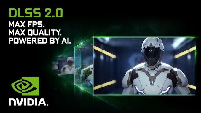
While NVIDIA’s annual GPU Technology Conference has been extensively dialed back and the bulk of NVIDIA’s announcements tabled for another day, as it turns out, the company still has an announcement up their sleeve this week. And a gaming-related announcement, no less. This morning NVIDIA is finally taking the wraps off of their DLSS 2.0 technology, which the company is shipping as a major update to their earlier AI-upscaling tech.


Responding to both competitive pressure and the realization of their own technology limitations, the latest iteration of NVIDIA’s upscaling technology is a rather significant overhaul of the technique. While NVIDIA is still doing AI upscaling at a basic level, DLSS 2.0 is no longer a pure upscaler; NVIDIA is now essentially combining it with temporal anti-aliasing. The results, NVIDIA is promising, is both better image quality than DLSS 1.0, as well as faster integration within individual games by doing away with per-game training.


As a quick refresher, Deep Learning Super Sampling (DLSS) was originally released around the launch of the Turing (GeForce RTX 20 series) generation in the fall of 2018. DLSS was NVIDIA’s first major effort to use their rapidly growing experience in AI programming and AI hardware to apply the technology to image quality in video games. With all of their GeForce RTX cards shipping with tensor cores, what better way to put them to use than to use them to improve image quality in games in a semi-abstracted manner? It was perhaps a bit of a case of a hammer in search of a nail, but the fundamental idea was reasonable, especially as 4K monitors get cheaper and GeForce 2080 Tis do not.


Unfortunately, DLSS 1.0 never quite lived up to its promise. NVIDIA took a very image-centric approach to the process, relying on an extensive training program that involved creating a different neural network for each game at each resolution, training the networks on what a game should look like by feeding them ultra-high resolution, 64x anti-aliased images. In theory, the resulting networks should have been able to recognize how a more detailed world should work, and produce cleaner, sharper images accordingly.


Sometimes this worked well. More often the results were mixed. NVIDIA primarily pitched the technology as a way to reduce the rendering costs of higher resolutions – that is, rendering a game at a lower resolution and then upscaling – with a goal of matching a game’s native resolution with temporal anti-aliasing. The end results would sometimes meet or beat this goal, and at other times an image would still be soft and lacking detail, revealing its lower-resolution origins. And all the while it took a lot of work to add DLSS to a game: every game and every resolution supported required training yet another neural network. Meanwhile, a simple upscale + sharpening filter could deliver a not-insignificant increase in perceived image quality with only a fraction of the work and GPU usage.


Enter DLSS 2.0


While DLSS 1.0 was pure, in retrospect it was perhaps a bit naïve. As NVIDIA plainly states now, DLSS 1.0 was hard to work with because it hinged on the idea that video games are deterministic – that everything would behave in a pre-defined and predictable manner. In reality games aren’t deterministic, and even if AI characters do the same thing every time, second-order effects like particles and the like can be off doing their own thing. As a result it was difficult to train DLSS 1.0 networks, which needed this determinism to improve, let alone applying them to games.


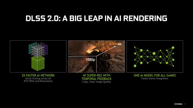
So for their second stab at AI upscaling, NVIDIA is taking a different tack. Instead of relying on individual, per-game neural networks, NVIDIA has built a single generic neural network that they are optimizing the hell out of. And to make up for the lack of information that comes from per-game networks, the company is making up for it by integrating real-time motion vector information from the game itself, a fundamental aspect of temporal anti-aliasing (TAA) and similar techniques. The net result is that DLSS 2.0 behaves a lot more like a temporal upscaling solution, which makes it dumber in some ways, but also smarter in others.


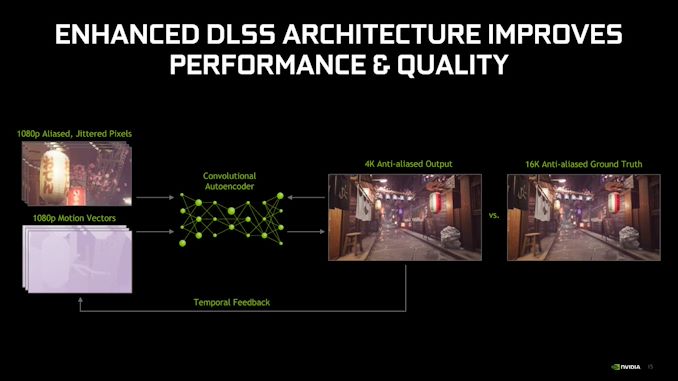
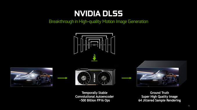
The single biggest change here is of course the new generic neural network. Looking to remove the expensive per-game training and the many (many) problems that non-deterministic games presented in training, NVIDIA has moved to a single generic network for all games. This newer neural network is based on a fully synthetic training set rather than individual games, which in turn is fully deterministic, allowing NVIDIA to extensively train the new network in exactly fashion they need for it to iterate and improve over generations. According to NVIDIA, this new network is also faster to execute on the GPU as well, reducing the overhead from using DLSS to begin with.


Besides eliminating per-game training times and hassling developers on determinism, the other upshot for NVIDIA is that the generic network gives them more resolution scaling options. NVIDIA can now upscale frames by up to 4x in resolution – from 1080p input to 4K – both allowing DLSS 2.0 to be used with a wider range of input/output resolutions, and allowing it to be more strongly used, for lack of a better term. DLSS 1.0, by contrast, generally targeted a 2x upscale.


This new flexibility also means that NVIDIA is now offering multiple DLSS quality modes, trading off the internal rendering resolution (and thus image quality) for more performance. Those modes are performance, balanced, and quality.


Otherwise, the actual network training process hasn’t entirely changed. NVIDIA is still training against 16K images, with the goal of teaching the neural network as much about quality as possible. And this is still being executed as neural networks via the tensor cores as well, though I’m curious to see if DLSS 2.0 pins quite as much work to the tensor cores as 1.0 did before it.


The catch to DLSS 2.0, however, is that this still requires game developer integration, and in a much different fashion. Because DLSS 2.0 relies on motion vectors to re-project the prior frame and best compute what the output image should look like, developers now need to provide those vectors to DLSS. As many developers are already doing some form of temporal AA in their games, this information is often available within the engine, and merely needs to be exposed to DLSS. None the less, it means that DLSS 2.0 still needs to be integrated on a per-game basis, even if the per-game training is gone. It is not a pure, end-of-chain post-processing solution like FXAA or combining image sharpening with upscaling.


Past that, it should be noted that NVIDIA is still defining DLSS resolutions the same way they were before; which is to say, they are talking about the output resolution rather than the input resolution. So 1080p Quality mode, for example, would generally mean the internal rendering resolution is one-half the output resolution, or 1280×720 being upscaled to 1920×1080. And Performance mode, I’m told, would be a 4x upscale.


Meanwhile, it goes without saying that the subject of image upscaling and enhancements has been a hot topic since the introduction of DLSS, as well as AMD’s more recent efforts to counter it with Radeon Image Sharpening. So NVIDIA is hitting the ground running, as it were, on promoting DLSS 2.0.


In fact “promotion” is perhaps the key word for today. While NVIDIA is only finally announcing DLSS 2.0 today and outlining how it works, the company has already been shipping it to game developers for a bit. Both Deliver Us the Moon and Wolfenstein: Youngblood are already shipping with DLSS 2.0. And now that NVIDIA is happy with the state of the now field-tested technology, they are moving on to rolling it out to gamers and game-developers as a whole, including integrating it into Unreal Engine 4.


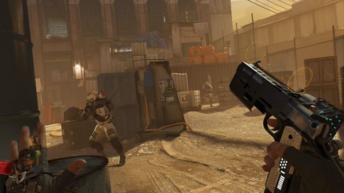
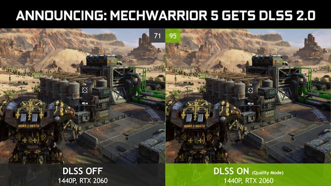
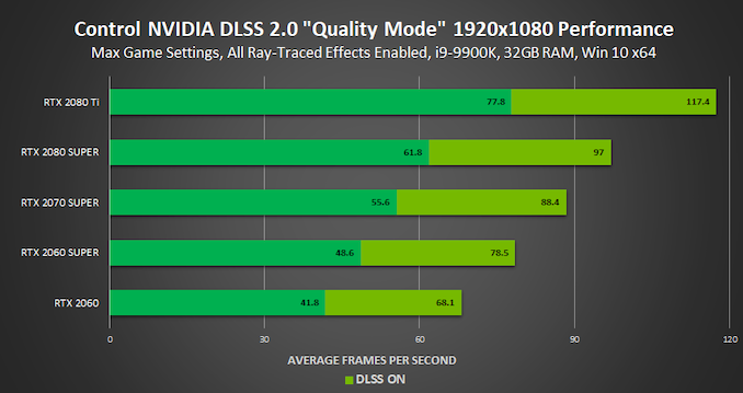
Along with the aforementioned games, both Control and MechWarrior 5 are getting DLSS 2.0 updates. Control in particular will be an interesting case, as it’s the only game in this set that also had a DLSS 1.x implementation, meaning that it can be used as a control to judge the image quality differences. Even NVIDIA is going that far to demonstrate some of the quality improvements.


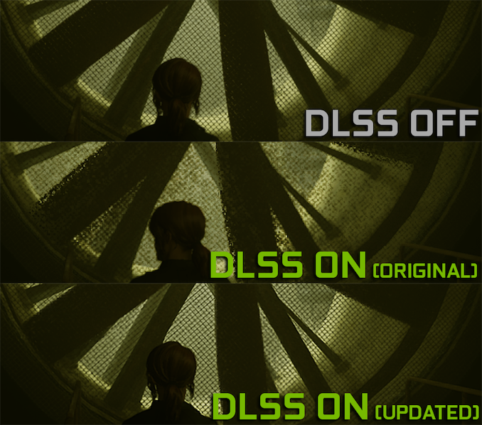
As for performance, NVIDIA is generally promising similar performance figures as DLSS 1.0. This means the comparable Quality mode may be a bit slower than DLSS 1.0 in games like Control, but overall that Quality mode and its one-half rendering resolution should deliver significant speed gains over native resolution games. All the while the resulting image quality should be better than what DLSS 1.0 could deliver. NVIDIA is even touting DLSS 2.0 as offering better image quality than native resolution games, though setting aside for the moment the subjective nature of image quality, it may not be quite an apples-to-apples comparison depending on what post-processing effects developers are using (e.g. replacing a very blurry TAA filter with DLSS 2.0).


At any rate, DLSS 2.0 is now officially available today. Updates for Control and MechWarrior 5 will be shipping this week, and if NVIDIA gets its way, more games will soon follow.


Source: AnandTech – NVIDIA Intros DLSS 2.0: Ditches Per-Game Training, Adds Motion Vectors for Better Quality

Samsung Galaxy S20+ & Ultra (Snapdragon & Exynos) Battery Life Preview

Last week we brought you a quick performance preview of the Snapdragon 865-based Samsung Galaxy S20 Ultra, showcasing that the phone has some outstandingly good performance and power efficiency statistics. Since then, we’ve been able to get our hands on an Exynos 990 based Galaxy S20+ and S20 Ultra, putting the trio of phones through our usual extensive review process.


We’re still working on the full big article which is still a week or more away, but we wanted already to cover one largest talking points about the new devices: battery life. Samsung’s new 120Hz refresh mode is quite a power-hungry beast, which alters the battery life formula for this year’s flagships. On top of that, we’re again seeing some quite large differences between the Exynos and Snapdragon based phones, and we’re able to report the first preliminary battery test results and analyse what the situation looks like.


Source: AnandTech – Samsung Galaxy S20+ & Ultra (Snapdragon & Exynos) Battery Life Preview

HMD Debuts First Nokia 5G Smartphone: The Nokia 8.3 5G with 4-Module Camera

HMD Global has announced their first Nokia-branded 5G-enabled smartphone, the Nokia 8.3 5G. Based on  Qualcomm’s Snapdragon 765G platform, Nokia is assembling a high-end smartphone that is designed to tick all of the required boxes for a good phone, while not driving quite as hard on features and prices as contemporary flagship smartphones. None the less, the large display phone packs a quad-sensor camera module, and in an interesting turn of events, it will support more 5G bands than other handsets on the market today.


Once released, the Nokia 8.3 5G will be one of the first handsets launched in the West that’s based on Qualcomm’s Snapdragon 765G system-on-chip, an interesting chip that, unlike the flagship Snapdragon 865, uses a fully integrated 5G modem. Furthermore, the 8.3 5G will be the very first phone that uses Qualcomm’s own 5G RF front-end module, a potentially important distinction as Qualcomm’s front-end supports a greater number of bands than other modules already on the market. As a result the 8.3 5G is being pitched as a “truly global” smartphone that should be able to work in most countries despite the wide disparity in which bands are used.


Otherwise, while the Snapdragon 765G is not Qualcomm’s flagship SoC, the recently-launched chip is still decidedly capable. The SoC uses two Cortex-A76 based CPU cores for high intensity workloads as well as a further six Cortex-A55 cores for low intensity workloads, and packs Qualcomm’s Adreno 620 integrated GPU. For the Nokia 8.3 5G, this is paired with 6 GB or 8 GB of LPDDR4X memory, as well as 64 GB or 128 GB NAND flash memory.


The first 5G Nokia handset comes with a large 6.81-inch IPS LCD with PureDisplay enhancements (deeper blacks, less reflections), and offers a 2400×1080 resolution (386 PPI). Oddly, however, HMD lists nothing about support for the DCI-P3 or HDR10 support, despite the fact that the company has supported HDR on earlier Nokia 7 and Nokia 8-series smartphones.


Instead, it’s imaging capabilities are often the strongest side of Nokia handsets, and HMD is aiming similarly high here. The Nokia 8.3 5G comes with a quad-sensor main camera module comprised of a 64 MP main sensor, a 12 MP ultrawide sensor, a 2 MP macro camera, and a 2 MP depth sensor. Nokia says that the main camera is tuned for better operation in low-light conditions and has some additional enhancements by Zeiss, who is also certifying the lenses. As for selfies, the smartphone has a punch-hole 24 MP camera on the front. And audio recording is provided via a Ozo surround audio microphone array.


When it comes to wireless connectivity, the Nokia 8.3 5G smartphone supports Wi-Fi 5, Bluetooth 5.0, and NFC. Meanwhile, the handset has a headphone jack as well as a USB 2.0 Type-C connector for data connectivity and charging. As for security, the device carries a fingerprint reader on its side.


Nokia’s handsets are known for their fine industrial design, so the Nokia 8.3 5G is clearly not an exception. The device has a rounded back and comes in Polar Night color that was inspired by Aurora Borealis usually seen in Norther Finland. Meanwhile, the phone is rather thick at nearly 9 mm and heavy at 220 grams. Otherwise, it should be noted that HMD isn’t listing the phone as offering any IP-grade water or dust resistance.


The Nokia 8.3 5G
  Nokia 8.3 5G

6/64
Nokia 8.3 5G

8/128
SoC Qualcomm Snapdragon 765G

1x Kryo 475 Prime (A76) @ 2.40 GHz

1x Kryo 475 Gold (A76) @ 2.20 GHz

6x Kryo 475 (A55) @ 1.80 GHz
GPU Adreno 620
DRAM 6 GB LPDDR4X 8 GB LPDDR4X
Storage 64 GB

microSD
128 GB

microSD
Display 6.81″ IPS LCD PureDisplay

2400 × 1080 (20:9)

386 PPI
Size Height 171.90 mm
Width 78.56 mm
Depth 8.99 mm
Weight 220 grams
Battery Capacity 4500 mAh
Wireless Charging ? ?
Rear Cameras
Main 64 MP

f/1.7

PDAF
UltraWide 12 MP 1/2.4″

f/2.2 13mm

?° field of view
Macro 2 MP
Depth 2 MP
Flash Dual-LED
Front Camera 24 MP

f/2.0
I/O USB 2.0 Type-C

Fingerprint reader on the side

Google Assistant button
Wireless (local) Wi-Fi 5

Bluetooth 5.0
Cellular GSM, CDMA, HSPA, 4G/LTE (1200/150 Mbps), 5G (2.4/1.2 Gbps)
Splash, Water, Dust Resistance ? ?
Dual-SIM Single nano-SIM or Dual nano-SIM
Launch OS Android 10
Launch Price €599 €649

HMD plans to make its Nokia 8.3 5G available this summer. The more affordable version with 6 GB of RAM and 64 GB of NAND will cost €599, whereas the more advanced model with 8 GB of RAM and 128 GB of NAND will be priced at €649.


Related Reading:


Sources: HMD Global, GSMArena


Source: AnandTech – HMD Debuts First Nokia 5G Smartphone: The Nokia 8.3 5G with 4-Module Camera

TerraMaster D5 Thunderbolt 3: A ‘Mega DAS’ with 5 Bays for 80 TB

TerraMaster this week introduced its first DAS featuring a Thunderbolt 3 interface. The D5 Thunderbolt 3 DAS with five bays is aimed at professionals who need a vast storage space attached directly to their PC. Using currently available hard drives, the D5 can store 80 TB of data, with peak sequential read speeds up to 1035 MB/s.


As the name suggests, the TerraMaster D5 Thunderbolt 3 can accommodate five 2.5-inch/3.5-inch hard drives or solid-state drives that can work in JBOD, RAID 0, RAID 1, RAID 5, and RAID 10 modes to provide various levels of performance and data protection capabilities. The DAS fully supports all RAID features one expects from a professional-grade storage device (see the table below) that has to ensure maximum reliability, predictable read/write speeds, and automatic RAID rebuild if needed.


Speaking performance, TerraMaster rates its D5 Thunderbolt 3 at up to 1035 MB/s read speed as well as up to 850 MB/s write speed. Such performance levels were measured by the manufacturer using a 5-disk SATA SSD array in RAID 0 mode. To ensure consistent performance and reliability, the DAS has two 80-mm fans.


As far as connectivity is concerned, the TerraMaster D5 Thunderbolt 3 DAS has two Thunderbolt 3 ports to daisy chain it with other TB3 devices as well as a DisplayPort 1.2 output.


Just like many other DAS, the D5 Thunderbolt 3 has a handle as many professionals need a lot of storage space while working outside of their home or office. The box itself weighs 2.3 kilograms, but when fully populated with high-capacity HDDs it will be considerably heavier.


TerraMaster D5 Thunderbolt 3 DAS will be available shortly. Pricing is unknown.


Related Reading


Sources: TerraMaster


Source: AnandTech – TerraMaster D5 Thunderbolt 3: A ‘Mega DAS’ with 5 Bays for 80 TB

Embedded 1.8-inch Zen PC: DFI Unveils Credit Card-Sized AMD Ryzen Board

DFI has announced what they consider the world’s smallest single-board computer (SBC) that uses on AMD’s Ryzen Embedded processor. The highly-integrated credit card-sized GHF51 motherboard can be used for a variety of applications that have to be small, yet offer capabilities as well as performance of a modern PC.


The DFI GHF51 1.8-inch platform carries AMD’s dual-core Ryzen Embedded R1000-series SoC with AMD Radeon Vega GPU featuring three compute units (192 stream processors) with hardware H.264, H.265, and VP9 decoding. The SoC can be paired with 2/4/8 GB of single-channel DDR4-3200 memory as well as 16/32/64 GB of eMMC storage. The SBC features one Mini PCIe slot for an add-in card, an 8-pin DIO header, two micro HDMI 1.4 outputs (4Kp30), one USB 3.2 Gen 2 Type-C port, a GbE connector (controlled by the Intel I211AT or the I210IT chip), and an fTPM 2.0 chip.


At present, DFI lists two AMD Ryzen-powered SBCs: the GHF51-BN-43R16 with the Ryzen Embedded R1606G APU (2.60 GHz – 3.50 GHz, 12 W) as well as the GHF51-BN-43R15 with the Ryzen Embedded R1505G APU (2.40 GHz – 3.30 GHz, 12 W). Both boards carry 4 GB of DDR4-3200 memory, 32 GB of eMMC storage, two micro HDMI outputs, a GbE port, and one USB 3.1 Gen 2 Type-C port. Eventually, the company plans to add motherboards powered by the lower-power Ryzen Embedded R1102G (1.20 GHz – 2.60 GHz, 6 W) or Ryzen Embedded R1305G (1.50 GHz – 2.80 GHz, 8/10 W) SoCs into the lineup in a bid to address applications that have to be less power hungry.


DFI’s GHF51 SBC is an example when AMD’s Ryzen Embedded enters the small form factor embedded market. The 1.8-inch SBCs can power various small form-factor or IoT applications that can take advantage of high-performance Zen cores, but theoretically they can also be used inside devices that currently use Raspberry Pi or similar. Obviously, a Ryzen Embedded SBC will probably cost more than a Raspberry Pi, but it will also provide higher performance, which opens doors to new use cases.


DFI has not announced pricing of its AMD Ryzen Embedded-based SBCs or their availability dates. In fact, the GHF51 product page currently mentions ‘Preliminary’ status of the boards.


Related Reading


Sources: DFI


Source: AnandTech – Embedded 1.8-inch Zen PC: DFI Unveils Credit Card-Sized AMD Ryzen Board

Logitech’s Combo Touch Keyboards, with Trackpad, for the 10.5-Inch iPad, Air and Pro

With Apple’s iPadOS 13.4 bringing trackpad support to the operating system, it was just a matter of time before third-party accessory manufacturers created new keyboards with a touchpad. Logitech with its Combo Touch keyboard cases turned out to be the first.


Logitech’s Combo Touch folios are full-sized keyboards designed for iPads, so they have all the iPadOS shortcut keys, a touchpad that supports all the gestures the operating system does (including swipe, scroll, switch apps, pinch, double-tap, and more), and has a kickstand supporting various angles. The keyboards use 18 mm keys featuring a scissor mechanism with a 1 mm travel distance and backlighting, so from this standpoint the Combo Touch behave exactly like Apple’s latest Magic Keyboards. Logitech’s keyboard cases can work with the company’s Control app that can adjust lighting as well as make firmware updates.


The biggest selling feature of the Logitech Combo Touch keyboard cases is their compatibility with 10.5-inch Apple’s tablets that have a Smart Connector. This includes the 7th Generation iPad, the 3rd Generation iPad Air, and iPad Pro 10.5-Inch. By contrast, Apple has so far only released its Magic Keyboard for its iPad Pro 11-inch as well as iPad Pro 12.9-inch.


Logitech’s Combo Touch Keyboard Cases for 10.5-Inch iPads
Model Compatibility Color Features Weight
920-009602 iPad 7th Generation Graphite 18-mm key pitch

1-mm travel time
610 grams
920-009606 iPad Air 3rd Gen

iPad Pro 10.5-Inch

The Logitech Combo Touch products are set to be available this May for $149.99 (which is two times lower than the price of Apple’s own Magic Keyboard for iPad Pro 11-inch that is set to cost $299.99, and $200 cheaper than the MSRP of the Magic Keyboard for iPad Pro 12.9-inch).


Related Reading:


Source: Logitech


Source: AnandTech – Logitech’s Combo Touch Keyboards, with Trackpad, for the 10.5-Inch iPad, Air and Pro

Quick Note: AMD Shows Off Raytracing on RDNA2

With today’s announcement from Microsoft of DirectX 12 Ultimate, both NVIDIA and AMD are also chiming in to reiterate their support for the new feature set, and to note their involvement in the process. For AMD, DirectX 12 Ultimate goes hand-in-hand with their forthcoming RDNA2 architecture, which will be at the heart of the Xbox Series X console, and will be AMD’s first architecture to support DirectX 12 Ultimate’s new features, such as ray tracing and variable rate shading.


To that end, as part of Microsoft’s overall DirectX Developer Day presentation, AMD is showing off raytracing running on an RDNA2 for the first time in public. Running an AMD-built demo they call “Futuristic City”, the demo incorporates DXR 1.0 and 1.1 features, to produce what can only be described as a very shiny demo.


It should be noted that this demo was a recording – as all of the Microsoft dev day presentations were – though there is little reason to doubt its authenticity. AMD also showed off an RT recording a couple of weeks back for Financial Analyst day, and presumably this is the same trailer.


Source: AnandTech – Quick Note: AMD Shows Off Raytracing on RDNA2

Microsoft Unveils DirectX 12 Ultimate: The GPU Feature Set For the Next Generation of Games

While the 2020 Game Developers Conference has been postponed, that thankfully doesn’t mean everything gaming-related for this spring has been postponed as well. As the saying goes, the show must go on, and this week we’ve seen Microsoft, Sony, and others go ahead and make some big announcements about their gaming consoles and other projects. Not to be left out of the fray, there is PC-related news coming out of the show as well.


Leading the PC pack this week is Microsoft (again), with the announcement of DirectX 12 Ultimate. Designed as a new, standardized DirectX 12 feature set that encapsulates the latest in GPU technology, DirectX 12 Ultimate is intended to serve as a common baseline for both PC game development and Xbox Series X development. This includes not only wrapping up features like ray tracing and variable rate shading into a single package, but then branding that package so that developers and the public at large can more easily infer whether games are using these cutting-edge features, and whether their hardware supports it. And, of course, this allows Microsoft to maximize the synergy between PC gaming and their forthcoming console, giving developers a single feature set to base their projects around while promoting the fact that the latest Xbox will support the very latest GPU features.


Source: AnandTech – Microsoft Unveils DirectX 12 Ultimate: The GPU Feature Set For the Next Generation of Games