AMD Scores First Top 10 Zen Supercomputer… at NVIDIA

One of the key metrics we’ve been waiting for since AMD launched its Zen architecture was when it would re-enter the top 10 supercomputer list. The previous best AMD system, built on Opteron CPUs, was Titan, which held the #1 spot in 2012 but slowly dropped out of the top 10 by June 2019. Now, in June 2010, AMD scores a big win for its Zen 2 microarchitecture by getting to #7. But there’s a twist in this tale.


Source: AnandTech – AMD Scores First Top 10 Zen Supercomputer… at NVIDIA

New #1 Supercomputer: Fujitsu’s Fugaku and A64FX take Arm to the Top with 415 PetaFLOPs

High performance computing is now at a point in its existence where to be the number one, you need very powerful, very efficient hardware, lots of it, and lots of capability to deploy it. Deploying a single rack of servers to total a couple of thousand cores isn’t going to cut it. The former #1 supercomputer, Summit, is built from 22-core IBM Power9 CPUs paired with NVIDIA GV100 accelerators, totaling 2.4 million cores and consuming 10 MegaWatts of power. The new Fugaku supercomputer, built at Riken in partnership with Fujitsu, takes the top spot on the June 2020 #1 list, with 7.3 million cores and consuming 28 MegaWatts of power.


Source: AnandTech – New #1 Supercomputer: Fujitsu’s Fugaku and A64FX take Arm to the Top with 415 PetaFLOPs

The Apple WWDC 2020 Keynote Live Blog (Starts at 10am PT/17:00 UTC)

While COVID may have put a crimp on the tech industry, for Apple the show must still go on. Join us at 10am Pacific/17:00 UTC for our live blog coverage of this year’s Apple WorldWide Developer’s Conference (WWDC), which like so many other shows is taking a uniquely virtual tack this year.


The morning keynote for the developer-focused show is typically a rapid-fire two-hour run through Apple’s ecosystem, covering everything from macOS and iOS to individual Apple applications and more, and it sounds like Apple will be sticking to that strategy for their virtual show. Meanwhile there’s always the lingering question over whether we’ll also see a new hardware announcement this year – Apple tends to be about 50/50 with hardware at WWDC – something which has taken on an even greater significance this year as Apple is widely believed to be working on transitioning the Mac platform to its own Arm-based SoCs. Even if we don’t get hardware details at this year’s WWDC, even confirmation of that project and Apple’s transition plans would mark the kick-off point for a huge shift in the Apple ecosystem, and an event that could reverberate into the PC ecosystem as well.


So join us at 10am Pacific to see just what Apple is working on for this year and beyond.


Source: AnandTech – The Apple WWDC 2020 Keynote Live Blog (Starts at 10am PT/17:00 UTC)

Intel to use Nanowire/Nanoribbon Transistors in Volume ‘in Five Years’

This year, at the international VLSI conference, Intel’s CTO Mike Mayberry gave one of the plenary presentations, which this year was titled ‘The Future of Compute’. Within the presentation, a number of new manufacturing technologies were discussed, including going beyond FinFET to Gate-All-Around structures, or even to 2D Nano-sheet structures, before eventually potentially leaving CMOS altogether. In the Q&A at the end of the presentation, Dr. Mayberry stated that he expects nanowire transistors to be in high volume production within five years, putting a very distinctive mark in the sand for Intel and others to reach.


Source: AnandTech – Intel to use Nanowire/Nanoribbon Transistors in Volume ‘in Five Years’

NVIDIA Announces PCIe A100 Accelerator: 250 Watt Ampere In A Standard Form Factor

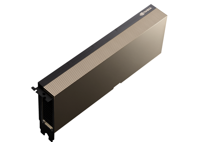
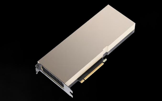
With the launch of their Ampere architecture and new A100 accelerator barely a month behind them, NVIDIA this morning is announcing the PCIe version of their accelerator as part of the start of the now-virtual ISC Digital conference for high performance computing. The more straight-laced counterpart to NVIDIA’s flagship SXM4 version of the A100 accelerator, the PCie version of the A100 is designed to offer A100 in a more traditional form factor for customers who need something that they can plug into standardized servers. Overall the PCIe A100 offers the same peak performance as the SXM4 A100, however with a lower 250 Watt TDP, real-world performance won’t be quite as high.


The obligatory counterpart to NVIDIA’s SXM form factor accelerators, NVIDIA’s PCIe accelerators serve to flesh out the other side of NVIDIA’s accelerator lineup. While NVIDIA would gladly sell everyone SXM-based accelerators – which would include the pricey NVIDIA HGX carrier board – there are still numerous customers who need to be able to use GPU accelerators in standard, PCIe-based rackmount servers. Or for smaller workloads, customers don’t need the kind of 4-way and higher scalability offered by SXM-form factor accelerators. So with their PCIe cards, NVIDIA can serve the rest of the accelerator market that their SXM products can’t reach.


The PCIe A100, in turn, is a full-fledged A100, just in a different form factor and with a more appropriate TDP. In terms of peak performance, the PCIe A100 is just as fast as its SXM4 counterpart; NVIDIA this time isn’t shipping this as a cut-down configuration with lower clockspeeds or fewer functional blocks than the flagship SXM4 version. As a result the PCIe card brings everything A100 offers to the table, with the same heavy focus on tensor operations, including the new higher precision TF32 and FP64 formats, as well as even faster integer inference.


NVIDIA Accelerator Specification Comparison
  A100

(PCIe)
A100

(SXM4)
V100

(PCIe)
P100

(PCIe)
FP32 CUDA Cores 6912 6912 5120 3584
Boost Clock 1.41GHz 1.41GHz 1.38GHz 1.3GHz
Memory Clock 2.4Gbps HBM2 2.4Gbps HBM2 1.75Gbps HBM2 1.4Gbps HBM2
Memory Bus Width 5120-bit 5120-bit 4096-bit 4096-bit
Memory Bandwidth 1.6TB/sec 1.6TB/sec 900GB/sec 720GB/sec
VRAM 40GB 40GB 16GB/32GB 16GB
Single Precision 19.5 TFLOPs 19.5 TFLOPs 14.1 TFLOPs 9.3 TFLOPs
Double Precision 9.7 TFLOPs

(1/2 FP32 rate)
9.7 TFLOPs

(1/2 FP32 rate)
7 TFLOPs

(1/2 FP32 rate)
4.7 TFLOPs

(1/2 FP32 rate)
INT8 Tensor 624 TOPs 624 TOPs N/A N/A
FP16 Tensor 312 TFLOPs 312 TFLOPs 112 TFLOPs N/A
TF32 Tensor 156 TFLOPs 156 TFLOPs N/A N/A
Relative Performance (SXM Version) 90% 100% N/A N/A
Interconnect NVLink 3

6 Links? (300GB/sec?)
NVLink 3

12 Links (600GB/sec)
NVLink 2

4 Links (200GB/sec)
NVLink 1

4 Links (160GB/sec)
GPU A100

(826mm2)
A100

(826mm2)
GV100

(815mm2)
GP100

(610mm2)
Transistor Count 54.2B 54.2B 21.1B 15.3B
TDP 250W 400W 250W 300W
Manufacturing Process TSMC 7N TSMC 7N TSMC 12nm FFN TSMC 16nm FinFET
Interface PCIe 4.0 SXM4 PCIe 3.0 SXM
Architecture Ampere Ampere Volta Pascal

But because the dual-slot add-in card form factor is designed for lower TDP products, offering less room for cooling and typically less access to power as well, the PCIe version of the A100 does have to ratchet down its TDP from 400W to 250W. That’s a sizable 38% reduction in power consumption, and as a result the PCIe A100 isn’t going to be able to match the sustained performance figures of its SXM4 counterpart – that’s the advantage of going with a form factor with higher power and cooling budgets. All told, the PCIe version of the A100 should deliver about 90% of the performance of the SXM4 version on single-GPU workloads, which for such a big drop in TDP, is not a bad trade-off.


And on this note, I should give NVIDIA credit where credit is due: unlike the PCIe version of the V100 accelerator, NVIDIA is doing a much better job of documenting these performance differences. This time around NVIDIA is explicitly noting the 90% figure in their their specification sheets and related marketing materials. So there should be a lot less confusion about how the PCIe version of the accelerator compares to the SXM version.


Other than the form factor and TDP changes, the only other notable deviation for the PCIe A100 from the SXM version is the number of NVLink-connected GPUs supported. For their PCIe card NVIDIA is once again using NVLink bridges connected across the top of A100 cards, allowing for two (and only two) cards to be linked together. NVIDIA’s product sheet doesn’t list the total bandwidth available, but as the PCIe V100 supported up to 100GB/sec in each direction using two links, the PCIe A100 and its 3 NVLink connectors should be able to do 150GB/sec, if not more.


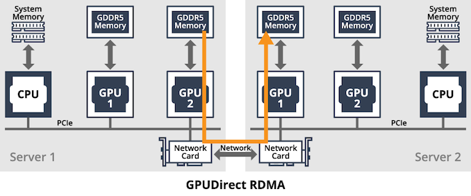
Otherwise the PCIe A100 comes with the usual trimmings of the form factor. The card is entirely passively cooled, designed to be used with servers with powerful chassis fans. And though not pictured in NVIDIA’s official shots, there are sockets for PCIe power connectors. Meanwhile, with the reduced usage of NVLink in this version of the card, A100’s native PCIe 4 support will undoubtedly be of increased importance here, underscoring the advantage that an AMD Epyc + NVIDIA A100 pairing has right now since AMD is the only x86 server vendor with PCIe 4 support.


Wrapping things up, while NVIDIA isn’t announcing specific pricing or availability information today, the new PCIe A100 cards should be shipping soon. The wider compatibility of the PCIe card has helped NVIDIA to line up over 50 server wins at this point, with 30 of those servers set to ship this summer.


Source: AnandTech – NVIDIA Announces PCIe A100 Accelerator: 250 Watt Ampere In A Standard Form Factor

GIGABYTE’s 4U 10x NVIDIA A100 New G492 Servers Announced

One of the interesting elements about NVIDIA’s A100 card is the potential compute density offered, especially for AI applications. There is set to be a strong rush to enable high-density AI platforms that can take advantage of all the new features that A100 offers in the PCIe form factor, and GIGABYTE was the first in my inbox with news of its new G492 server systems, built to take up to 10 new A100 accelerators. These machines are built on AMD EPYC, which allows for PCIe Gen4 support, as well as offering GPU-to-GPU direct access, direct transfers, and GPUDirect RDMA.


The G492 servers use dual EPYC CPUs, allowing for 128 PCIe 4.0 lanes in total, however in order to expand support to 10 GPUs as well as up to 12 additional NVMe storage drives, PCIe 4.0 switches are used (Broadcom PEX9000 in the G492-Z51, Microchip in the G492-Z50). This also allows an additional three PCIe x16 links and an OCP 3.0 slot for add-on upgrade cards for SAS drives or networking, such as Ethernet or Mellanox Infiniband.


The use of dual EPYC CPUs, up to 280W each, also allows for up to 8 TiB of DDR4-3200 memory support. The system comes with three 2200W 80 PLUS Platinum redundant power supplies. The 10 GPU slots are rated for 250W TDP a piece, and the system comes equipped with dual 10 GBase-T and AST2500 management as standard.


Gigabyte customers interested in deploying G492 should get in contact with their local distributor.


Source: GIGABYTE


Related Reading


Source: AnandTech – GIGABYTE’s 4U 10x NVIDIA A100 New G492 Servers Announced

Mobile Flagship Phone Camera Overview 2020 H1: Still Picture Battle

These days whenever you select a flagship smartphone, you generally get more or less the same fundamental formula no matter the vendor you chose. It’s a glass slab with a screen, and more often than not even the internal hardware powering the phones isn’t all that different, with just a few exceptions. Whilst most vendors try to differentiate themselves in their designs and ergonomics – some with more success than others – the one aspect where smartphones can still be very different from each other is their cameras.

This year we’ve seen smartphones with more variety than ever in terms of their camera setups. The last few years has seen an explosion of fast-paced innovation in the image capture abilities of smartphones, with vendors focusing on this last aspect of a phone where they can truly differentiate themselves from others, and try to one-up the competition.

We’re halfway through 2020, and almost all vendors have released their primary flagship devices – many of which we still had yet to cover in full reviews. This was a perfect opportunity to put all of the new generation devices against each other and compare their cameras systems to really showcase just how different (or similar) they are to each other. Today’s article is a battle-royale for smartphone photography, providing an apples-to-apples comparison across the most important devices available today.


Source: AnandTech – Mobile Flagship Phone Camera Overview 2020 H1: Still Picture Battle

Intel Launches Cooper Lake: 3rd Generation Xeon Scalable for 4P/8P Servers

We’ve known about Intel’s Cooper Lake platform for a number of quarters. What was initially planned, as far as we understand, as a custom silicon variant of Cascade Lake for its high-profile customers, it was subsequently productized and aimed to be inserted into a delay in Intel’s roadmap caused by the development of 10nm for Xeon. Set to be a full range update to the product stack, in the last quarter, Intel declared that its Cooper Lake platform would end up solely in the hands of its priority customers, only as a quad-socket or higher platform. Today, Intel launches Cooper Lake, and confirms that Ice Lake is set to come out later this year, aimed at the 1P/2P markets.


Source: AnandTech – Intel Launches Cooper Lake: 3rd Generation Xeon Scalable for 4P/8P Servers

Intel Announces D7-P5500 and D7-P5600 Series PCIe 4.0 Enterprise SSDs

Intel has yet to launch their first CPUs supporting PCIe 4.0, but other parts of the business are keeping pace with the transition: network controllers, FPGAs, and starting today, SSDs. The first PCIe 4.0 SSDs from Intel are based on their 96-layer 3D TLC NAND flash memory, slotting into Intel’s product line just below Optane products and serving as Intel’s top tier of flash-based SSDs. The new Intel D7-P5500 and D7-P5600 are codenamed Arbordale Plus, a codename Intel revealed last fall without providing any other information except that the original Arbordale product was never released.


The two new SSD product lines are the first to fall into the D7 tier under the new naming scheme adopted by Intel in 2018. The P5500 and P5600 are closely-related products that differ primarily in their overprovisioning ratios and consequently their usable capacities, write speed and write endurance. The P5500 is the 1 drive write per day (DWPD) lineup with capacities ranging from 1.92 TB up to 7.68 TB, while the P5600 is the 3 DWPD tier with capacities from 1.6 TB to 6.4 TB. These serve as the successors to the P4510 and P4610 Cliffdale Refresh drives, and as such we expect some follow-on models to introduce the EDSFF form factor options and QLC-based drives that are still due for an update.


Intel PCIe 4.0 Enterprise SSDs
  D7-P5500 D7-P5600
Form Factor U.2 2.5″ 15mm
Interface PCIe 4.0 NVMe 1.3c
Capacities 1.92TB,

3.84TB,

7.68TB
1.6TB,

3.2TB,

6.4TB
NAND Intel 96L 3D TLC
Sequential Read 7000 MB/s
Sequential Write 4300 MB/s
Random Read (4 kB) 1M IOPS
Random Write (4 kB) 130k IOPS 260k IOPS
Power Idle 20 W
Operating 5 W
Write Endurance 1 DWPD 3 DWPD
Warranty 5 years

The switch to PCIe 4.0 enables a big jump in maximum throughputs supported: from 3.2 GB/s up to 7 GB/s for sequential reads, while sequential writes show a more modest increase from 3.2 GB/s to 4.3 GB/s. Random reads now hit 1M IOPS compared to about 651k IOPS from the previous generation, and random writes are still bottlenecked by the flash itself with a peak of 260k IOPS from the new P5600.


Intel hasn’t shared information about the internal architecture of the new SSDs, so we don’t know if they’re still using a 12-channel controller design like their previous generation. Intel does tout improved QoS and a handful of new features, including a re-working of their TRIM implementation to reduce its interference with the performance of more important IO commands.


Related Reading


Source: AnandTech – Intel Announces D7-P5500 and D7-P5600 Series PCIe 4.0 Enterprise SSDs

The SilverStone Permafrost PF120, PF240, and PF360 ARGB AIO Coolers Review

SilverStone is a well-known name amongst advanced users and enthusiasts. The company earned its reputation from its first PSUs and original case designs, and soon diversified towards cooling related products. Their products usually are designed to be cost-effective, with a focus on practicality and quality instead of extravagant aesthetics. That tactic served SilverStone very well in the past, some of their CPU tower coolers have become very good values for the price.


Given SilverStone’s success with air coolers, today we are switching tracks to liquid coolers and taking a look at SilverStone’s latest all-in-one (AIO) “Permafrost” cooler series. With multiple models covering the most popular cooler sizes, SilverStone is looking to tap into what has continued to be a popular market for alternative high-performance coolers. And with the inclusion of Addressable RGB (ARGB) lighting, SilverStone is perhaps bowing to a bit to market pressures as well by including RGB lighting in their new AIO coolers.


Source: AnandTech – The SilverStone Permafrost PF120, PF240, and PF360 ARGB AIO Coolers Review

Lenovo’s New ThinkPad P1 Gen3 for Professionals: OLED, 8-core Xeon, Quadro

At the high-end of Lenovo’s ThinkPad designs, where professionals need server-grade features like ECC and graphics focused on compute or rendering, we get the P1 model which is updated for 2020 as the P1 Gen3. This notebook refresh is a 15.6-inch design, offering an OLED display, choice of Intel 10th Gen or Xeon processors, and Quadro-level graphics. The underlying design of the chassis is carbon fiber, aiming to be sturdy yet lightweight, with a fingerprint resistant finish to enhance the aesthetic of a premium system.


The ThinkPad P1 Gen3 is a 15.6-inch design with options that include a 3840×2160 OLED touch display at HDR500, a 3840×2160 LCD IPS variant up to 600 nits, or a 1920×1080 IPS 500nit HDR lower-cost option. Under the hood it supports Intel’s 10th Gen Core mobile 45 W processors, or their Xeon equivalents, which extends support to up to 64 GB of ECC for the Xeons via two SoDIMM slots. Graphics are available up to an NVIDIA Quadro T2000. There are two M.2 drives in the system, allowing for up to 4 TB of NVMe SSDs in RAID 0/1, and the system comes with an 80 Wh battery. Two power supplies are available – a base 135 W slim model or a 170 W slim model. Operating system options include Windows 10 Home, Pro, Pro for Workstations, Ubuntu, Red Hat (certified), or Fedora.


For professional users, the P1 Gen3 supports TPM, has a touch fingerprint reader for easy log-in, and a shutter mechanism for the 720p webcam. There is also an optional separate Hybrid IR camera. On the connectivity side, Intel’s AX201 Wi-Fi 6 solution is included as standard, but a CAT16 LTE smartphone modem is an optional extra, which comes in the M.2 form factor. The system is certified for a number of software vendors, such as AutoCAD, CATRIA, NX, SolidWorks, Revit, Creo, Inventor, etc.


From the design, the unit comes with the usual ThinkPad bells and whistles. The keyboard includes the TrackPoint in the middle of the keyboard, and the track pad at the bottom has physical keys above it. The keyboard is backlit and spill resistant. Ports on the side include two USB 3.2 Gen 1 Type-A ports, two USB-C Thunderbolt 3 ports, a HDMI 2.0 video output, a 3.5mm jack, and an SD Card Reader.


A suggested Lenovo Use Case


The P1 Gen3 comes with Lenovo’s ThinkShield software, and will also be the recipient of Lenovo’s new Ultra Performance Mode that allows the user to adjust the performance settings in order to achieve a desired performance or thermal characteristics of the system. Lenovo believes this is mostly relevant to users who need full turbo to get a project completed on time, or for those who use the system with VR and require a minimum standard of performance without any potential thermal disruptions.


The P1 Gen3 starting weight is 3.75 lbs (1.7 kg), which will add on with the addition of a graphics card / more memory / more storage etc. The Lenovo ThinkPad P1 Gen3 will be available from July, starting at $2019.


Source: AnandTech – Lenovo’s New ThinkPad P1 Gen3 for Professionals: OLED, 8-core Xeon, Quadro

Lenovo Unveils ThinkPad X1 Extreme Gen3: 45 W Core i9, 15.6-inch, 1650Ti

For the high-performance commercial space, the line of Extreme Lenovo ThinkPads is a popular choice. For the current generation, Lenovo is unveiling a new X1 Extreme Gen3 version specifically for those commercial users that need performance from both the CPU and GPU in a typical ThinkPad style design. Highlights include the Intel Core-H series processor, the optional NVIDIA GeForce 1650Ti graphics, a 600-nit 15.6-inch display, as well as Wi-Fi 6 capabilities and an optional Cat16 LTE modem.


The new ThinkPad rotates out to a full 180-degree stance, with the bottom of the screen helping left the laptop to create airflow when at a more userfriendly angle. The X1 Extreme Gen3 will have a multitude of ports, including a card reader, two Type-A ports, two Type-C ports, a built in full-sized HDMI port, a 3.5mm jack, and Lenovo’s custom power connector. The company hasn’t released all the specifications yet, so we might expect to see Thunderbolt 3 support and additional Type-C charging perhaps.


New to some of Lenovo’s designs is its new Ultra Performance Mode, which is set to be exclusive to the Extreme and the ThinkPad P series. This will cause the system to enable higher power limits and higher thermal limits, as well as locking the hardware in at high frequencies, such that when it is critical for a render to complete on time or for a VR experience to not drop, these systems are capable (noise and thermals permitting). It will be interesting to see what this does above the standard Windows Ultimate Performance power mode.


Unfortunately Lenovo isn’t releasing too many details on its new X1 Extreme Gen3 just yet, indicating that it was perhaps planning to show an early engineering sample at what would have been the traditional Computex trade show a couple of weeks ago. The company states that the ThinkPad X1 Extreme Gen3 will be available from July, Price TBD.


Source: AnandTech – Lenovo Unveils ThinkPad X1 Extreme Gen3: 45 W Core i9, 15.6-inch, 1650Ti

Qualcomm Announces RB5 Robotics Platform – A Powerful SBC

Today Qualcomm is announced an update to its robotics platform, upgrading the aging RB3 with a Snapdragon 845-based SoC with the new RB5 platform which is based on a newer Snapdragon 865 chipset. Qualcomm is aiming for gaining market share in the fast-growing industry that’s projected to reach $170B by 2025.


What’s might be more interesting for AnandTech users, is the RB5’s potential as an Arm single-board computer platform, as the inclusion of the newest silicon here should represent a significant advantage for designs based on the RB5 platform and the Snapdragon 865 derived “QRB5165” chipset.


The design of the RB5 platform comes in the form of a carrier board and a system-on-module board. The SOM contains the actual SoC alongside core components such as RAM, NAND storage chip, the PMIC powering the SoC and board components, as well as a Wi-Fi/BT module.


The module sits on a carrier board, in this case the Qualcomm Robotics RB5 carrier board features a ton of connectivity, supporting 4x HDMI outputs, SD card slot via SDIO, USB 3.1 hub, USB-C connector, Gigabit-Ethernet, DSI and CSI connectors for attaching displays and cameras, and various other general purpose I/O. We also see inclusion of two lanes of PCIe included.


It’s possible to extend the “core kit” with various other add-ons in the form of extra mezzanine boards. Qualcomm will be offering a Vision, Sensor, Motor Control, Industrial, and Communications mezzanine boards for expanding the capabilities of the system.


The interesting aspect of the platform of course is its software support. Qualcomm will be offering OS support for both Ubuntu and Yocto Linux. The company will be maintaining its own downstream embedded variants of the operating systems, as well as offering upstream open-source versions. The QRB5165 will be seeing long life software support which extends to Linux.


These latter aspects of the platform make it a quite interesting value proposition for anybody who’s looking for an Arm development system. The Snapdragon 865 and the Cortex-A77 cores are extremely capable and would certainly give similar other SBCs offerings such as Nvidia’s Jetson dev kits a run for their money. Qualcomm hasn’t mentioned any pricing yet, but partner vendors such as Thundercomm are offering the previous generation RB3 basic kit for $449 – so we’d hope the RB5 would see similar pricing.


Source: AnandTech – Qualcomm Announces RB5 Robotics Platform – A Powerful SBC

Qualcomm Announces Snapdragon 690: 5G & A77 In The Mid-Range

Today Qualcomm is extending its 5G SoC portfolio down to the Snapdragon 600-series, introducing the new Snapdragon 690 platform and chip. The new design is a more significant upgrade to the 600-series, not only upgrading the cellular capabilities, but also upgrading some of the cornerstone IPs to the newest generation available.


Qualcomm Snapdragon 600-Range SoCs
SoC Snapdragon 660 Snapdragon 662 Snapdragon 665 Snapdragon 670 Snapdragon 675 Snapdragon 690
CPU 4x Kryo 260 (CA73)

@ 2.2GHz


4x Kryo 260 (CA53)

@ 1.8GHz

4x Kryo 260 (CA73)

@ 2.0GHz


4x Kryo 260 (CA53)

@ 1.8GHz

4x Kryo 260 (CA73)

@ 2.0GHz


4x Kryo 260 (CA53)

@ 1.8GHz

2x Kryo 360 (CA75)

@ 2.0GHz 


6x Kryo 360 (CA55)

@ 1.7GHz

2x Kryo 460 (CA76)

@ 2.0GHz


6x Kryo 460 (CA55)

@ 1.7GHz
2x Kryo 560 (CA77)

@ 2.0GHz


6x Kryo 560 (CA55)

@ 1.7GHz
GPU Adreno 512 Adreno 610 Adreno 615 Adreno 612 Adreno 619L
DSP Hexagon 680  Hexagon 683  Hexagon 686  Hexagon 686  Hexagon 685  Hexagon

692
ISP/

Camera
Spectra 160

24MP
Spectra 340T

25MP single / 16MP dual
Spectra 165

25MP single / 16MP dual
Spectra 250

25MP single / 16MP dual
Spectra 250

25MP single / 16MP dual
Spectra 355L

48MP single / 32+16MP dual
Memory 2x 16-bit @ 1866MHz

LPDDR4

14.9GB/s
2x 16-bit @ 1866MHz

LPDDR4X

14.9GB/s


1MB system cache

Integrated Modem Snapdragon X12 LTE Snapdragon X11 LTE

(Cat 12/13)


DL = 390Mbps

2x20MHz CA, 256-QAM


UL = 150Mbps

2x20MHz CA, 64-QAM

Snapdragon X12 LTE


(Category 12/13)


DL = 600Mbps

3x20MHz CA, 256-QAM


UL = 150Mbps

2x20MHz CA, 64-QAM

Snapdragon X51


( LTE )

DL = 1200 Mbps

UL = 210 Mbps


5G NR

Sub-6 
)

DL = 2500 Mbps

UL = 1200 Mbps

Encode/

Decode
2160p30, 1080p120

H.264 & H.265
1080p60

H.264 & H.265
2160p30, 1080p120

H.264 & H.265
Mfc. Process 14nm LPP 11nm LPP 11nm LPP 10nm LPP 11nm LPP 8nm LPP

Although the new Snapdragon 690 maintains its CPU configurations in terms of big and little cores in a 2+6 setup, Qualcomm has managed to include the newest Cortex-A77 IP for the big CPU cores, resulting in a 20% performance uplift thanks to the microarchitectural improvements. The clock speeds remain the same as found in other recent 600-series designs, meaning 2GHz on the big cores and 1.7GHz for the A55 cores.


On the GPU side, we see the shift to a new Adreno 619L design sees a much bigger shift with an up to 60% increase in performance compared to the previous generation Snapdragon 675.


Memory-wise, it’s still a LPDDR4X SoC with dual 16-bit channel support, which is plenty for the bandwidth requirements at this performance segment.


Qualcomm is also trickling down some of the newer higher end multimedia features to the 600-series, such as the newer generation Spectra iSP which is able to support up to 192MP still pictures or up to 48MP sensors with multi-frame noise reduction, or a dual-camera setup in tandem of 32+16MP sensors. The chip has a 10-bit capture and display pipeline, allowing it 4K HDR capture and display – although we didn’t see mention of 4K60 recording.


The key feature of the Snapdragon 690 is its shift towards a 5G modem platform. The integrated X51 modem now adds support for 5G sub-6GHz with global band support. The speeds here scale up to 2500Mbps downstream and 1200Mbps upstream on sub-6 networks, utilising up to 100MHz of spectrum bandwidth. The chip seemingly makes without mmWave connectivity, and this makes a lot of sense given the price range that the 600-series is meant to be used in, as well as the general lack of mmWave adoption in most markets.


“This new platform is designed to make 5G user experiences even more broadly available around the world. Snapdragon 690 also supports remarkable on-device AI and vibrant entertainment experiences. HMD Global, LG Electronics, Motorola, SHARP, TCL, and Wingtech are among the OEMs/ODMs expected to announce smartphones powered by Snapdragon 690.”


We’re expecting the new chip to be deployed in devices by various vendors in the second half of the year.


Related Reading:


Source: AnandTech – Qualcomm Announces Snapdragon 690: 5G & A77 In The Mid-Range

The AMD B550 Motherboard Overview: ASUS, GIGABYTE, MSI, ASRock, and Others

AMD’s budget motherboard range is often at times more successful than the bigger, full fat versions. Users have in the past got almost all of the same chipset features on these motherboards than they did on the X-series range. That changes with the new B500 series as consumers no longer have PCIe 4.0 on the chipset, instead reverting back to PCIe 3.0. This ultimately should not be an issue, as budget builds are unlikely to have multiple PCIe 4.0 add-in drives, for example. Nonetheless, the high vocal demand for B550 motherboards, especially after AMD launched Ryzen 3, has not gone unnoticed, and there are over 40 new models in the market, most of which should be on sale from today.


Source: AnandTech – The AMD B550 Motherboard Overview: ASUS, GIGABYTE, MSI, ASRock, and Others

Kioxia Launches PM6: First 24G SAS SSD, up to 30.72 TB

Kioxia (formerly Toshiba Memory) has launched their sixth generation enterprise SAS SSD, the PM6 series. This is the first SSD available to support the latest 24G SAS interface, doubling performance over the existing 12Gb/s SAS standard. Using 96-layer 3D TLC NAND flash memory, the PM6 offers capacities up to 30.72 TB and performance up to 4300 MB/s.


Serial-Attached SCSI (SAS) originated from the simple idea of running the enterprise-grade SCSI protocol over the Serial ATA physical layer, obsoleting parallel SCSI connections in the same way that SATA displaced parallel ATA/IDE in the consumer storage world. The first version of SAS corresponded to the second generation of SATA, with each running at 3 Gbit/s. SATA became a dead-end technology after one more speed increase to 6 Gbit/s, but SAS development has continued to higher speeds: 12Gbit SAS-3 was standardized in 2013 and “24G” SAS-4 was standardized in 2017. The “24G” is in quotes because SAS-4 actually runs at a raw rate of 22.5Gbit/s but delivers a true doubling of usable data rate by switching to lower-overhead error correction: 8b/10b encoding replaced with 128b/150b (actually 128/130 plus 20 bits of extra forward error correction), similar to how PCIe 3.0 switched from 8b/10b to 128b/130b to deliver 96% higher transfer rates with only a 60% increase in raw bit rate. Also similar to PCIe, it takes quite a while to go from release of the interface standard to availability of real products, which is why a 24G SAS SSD is only just now arriving.


Kioxia’s enterprise SAS SSDs and their enterprise NVMe SSDs share the same bilingual controller ASIC and consequently the PM6 has a very similar feature set to the previously-announced CM6 PCIe 4.0 SSDs. This includes dual-port interface support for higher performance or for fault tolerance, and enough ECC and parity protection for the drive to survive the failure of two entire flash dies. The SAS-based PM6 series is limited to lower maximum throughput than the CM6, but a dual-lane 24G SAS link is still slightly faster than PCIe 3.0 x4. The higher performance enabled by 24G SAS means the PM6 can require more power than its predecessors—now up to 18W, though the drive can be configured to throttle to lower power levels ranging from 9W to 14W.


Kioxia Enterprise SSD Specifications
Model PM6 SAS CM6 NVMe
Form Factor 2.5″ 15mm U.3
Interface, Protocol Dual-port 24G SAS PCIe 4.0 x4, NVMe 1.4
NAND Flash Kioxia 96L 3D TLC
Capacities (TB) 960GB,

1.92TB,

3.84TB,

7.68TB,

15.36TB
800GB,

1.6TB,

3.2TB,

6.4TB,

12.8TB
400GB,

800GB,

1.6TB,

3.2TB
960GB,

1.92TB,

3.84TB,

7.68TB,

15.36TB,

30.72TB
800GB,

1.6TB,

3.2TB,

6.4TB,

12.8TB
Write Endurance 1 DWPD 3 DWPD 10 DWPD 1 DWPD 3 DWPD
Sequential Read 4.3 GB/s 6.9 GB/s

The PM6 SAS family is available in three endurance tiers: the 1 DWPD and 3 DWPD models closely correspond to CM6 NVMe models, but only the SAS product line gets a 10 DWPD tier. Maximum capacities are 30.72 TB in the 1 DWPD series, 12.8 TB in the 3 DWPD series and 3.2 TB in the 10 DWPD series. Kioxia said that 4 TB class drives are still the most popular, but this will probably be shifting toward the 8 TB models over the next year or so. The 30.72 TB models will remain more of a niche product in the near future, but they expect demand for those capacities to start picking up in 2021 or 2022. Detailed performance specifications for each model are not yet available.


SAS in general is still a growing market both in terms of number of units and bits shipped and is projected to continue growing for at least a few more years, even though NVMe is gradually taking over the enterprise SSD market. Kioxia’s customer base for SAS SSDs has been divided between storage array vendors and the traditional enterprise server market. The storage array market has been quicker about migrating to NVMe so this may be the last generation of SAS SSDs to see significant adoption in that market segment. SAS will be hanging around in the enterprise server market for a lot longer, helped in part by the backwards-compatibility with SATA hard drives for cheap high-capacity storage, and the straightforward traditional RAID solutions as compared to the challenges with NVMe RAID. The server market typically doesn’t make as much use of the dual-port capability of SAS drives, so the speed boost from 24G SAS will be particularly welcome there, allowing drives to now reach about 2.3GB/s each rather than about 1.1GB/s on 12Gb SAS.


The Kioxia PM6 SAS SSDs are now available for customer qualification and evaluation. The drives have already been validated with 24G SAS host controllers from both Broadcom and Microchip (Microsemi/Adaptec).


Source: AnandTech – Kioxia Launches PM6: First 24G SAS SSD, up to 30.72 TB

AMD To Launch New Ryzen 3000 XT CPUs: Zen 2 with More MHz

One of the more frequent rumors in recent weeks has been that AMD would have some new Ryzen 3000 processors to launch. Today AMD is announcing three new processors into the Ryzen 3000 family, each with the XT name, offering higher frequencies and further filling out the their CPU product stack. Each of these processors will be available on shelves in primary regions on July 7th.


Source: AnandTech – AMD To Launch New Ryzen 3000 XT CPUs: Zen 2 with More MHz

AMD Announces Radeon Pro 5600M Navi GPU with HBM2 – Inside Apple's MacBook Pro 16"

Today AMD has officially announced one of the long rumoured missing Navi parts in the form of the new Radeon Pro 5600M mobile GPU, seeing the Navi 12 design finally take shape as a product.


The new high-end mobile GPU is a successor to the Radeon Pro Vega 20 and Vega 16 designs released back in 2018, products that ended up being used in Apple’s MacBook laptops. The new Radeon Pro 5600M also sees its debut in the new 16” MacBook Pro that’s also been debuted today. Apple has traditionally had exclusive rights to these mobile Radeon Pro SKUs so it’s likely this exclusivity also applies to the new Radeon Pro 5600M.


AMD Radeon Series Mobile Specification Comparison
  AMD Radeon Pro 5600M AMD Radeon RX 5300M AMD Radeon RX 5500M AMD Radeon Vega Pro 20 AMD Radeon RX 560X
CUs 40 22 22 20 14/16
Texture Units 160 88 88 80 64
ROPs ? 32 32 32 16
Game Clock N/A 1181MHz 1448MHz N/A N/A
Boost Clock 1035MHz 1445MHz 1645MHz 1300MHz 1275MHz
Throughput (FP32) 5.3 TFLOPs 4.1 TFLOPs 4.6 TFLOPs 3.3 TFLOPs 2.6 TFLOPs
Memory Clock 1.54 Gbps HBM2 14 Gbps GDDR6 14 Gbps GDDR6 1.5 Gbps HBM2 7 Gbps GDDR5
Memory Bus Width 2048-bit 96-bit 128-bit 1024-bit 128-bit
Max VRAM 8GB 3GB 4GB 4GB 4GB
Typical Board Power 50W ? 85W ? ?
Architecture RDNA (1) RDNA (1) RDNA (1) Vega

(GCN 5)
GCN 4
GPU Navi 12 Navi 14 Navi 14 Vega 12 Polaris 11
Launch Date Q2 2020 Q4 2019 Q4 2019 10/2018 04/2018

The new mobile GPU is characterised by its large compute unit count as well as its usage of HBM2 memory. With a CU count of 40, resulting in 2540 stream processors, the Radeon Pro 5600M actually matches AMD’s current best desktop graphics designs such as the Navi 10-based Radeon 5700XT. A key difference here lies in the clocks as this mobile variant only clocks up to a maximum of 1035MHz, resulting in a theoretical maximum throughput of 5.3TFLOPs, quite a bit less than its desktop counterpart which lands in at 9.75TFLOPs.


In terms of bandwidth however, the mobile chip more than keeps up with its desktop counterpart. AMD is using a 2048-bit HBM2 memory interface to up to 8GB of memory running at 1.54Gbps, resulting in a bandwidth of 394GB/s, only a bit less than the 448GB/s of the Radeon 5700XT.


The Radeon Pro 5600M is advertised with a total graphics power (TGP) of 50W, identical to the TGP of the Radeon Pro 5500M and the Radeon Pro 5300M, both based on the Navi 14 die which contains much less compute units. This makes the 5600M an incredibly performant and efficient design.


The new Radeon Pro 5600 is now available inside of Apple’s MacBook Pro 16” as an option, and comes at a $700 mark-up versus the default Radeon Pro 5500M GPU.


Related Reading:


Source: AnandTech – AMD Announces Radeon Pro 5600M Navi GPU with HBM2 – Inside Apple’s MacBook Pro 16″

Storage Matters: Why Xbox and Playstation SSDs Usher In A New Era of Gaming

A new generation of gaming consoles is due to hit the market later this year, and the hype cycle for the Xbox Series X and Playstation 5 has been underway for more than a year. Solid technical details (as opposed to mere rumors) have been slower to arrive, and we still know much less about the consoles than we typically know about PC platforms and components during the post-announcement, pre-availability phase. We have some top-line performance numbers and general architectural information from Microsoft and Sony, but not quite a full spec sheet.


The new generation of consoles will bring big increases in CPU and GPU capabilities, but we get that with every new generation and it’s no surprise when console chips get the same microarchitecture updates as the AMD CPUs and GPUs they’re derived from. What’s more special with this generation is the change to storage: the consoles are following in the footsteps of the PC market by switching from mechanical hard drives to solid state storage, but also going a step beyond the PC market to get the most benefit out of solid state storage. These are exciting times, to say the least.


To that end, today we’re taking a look at what to expect from the new console SSDs, as well as what it means for the gaming industry as a whole.


Source: AnandTech – Storage Matters: Why Xbox and Playstation SSDs Usher In A New Era of Gaming