Samsung Lets Note20+/Ultra Design Slip

We still haven’t had any official announcements from Samsung regarding the Note20 series as of yet, expecting the company to only reveal the new phone series sometime in early to mid-August if past release dates are any indications. Yet in a surprise blunder, the company has managed to publicly upload two product images of the upcoming Note20+ or Ultra (naming uncertain) on one of its Ukrainian pages.


Whilst we usually don’t report on leaks or unofficial speculations as part of our editorial standards – a first party blunder like this is very much an exception to the rule.


The leak showcases the seemingly bigger sibling of the Note20 series as it features the full camera housing and seemingly same modules as the Galaxy S20 Ultra. There’s been a design aesthetic change as the cameras are now accentuated by a ring element around the lenses, making the modules appear more consistent with each other, even though there’s still clearly different sized lenses along with the rectangular periscope zoom module. The images showcase actual depth on the part of the ring elements, so they may extend in three dimensions.


The new gold/bronze colour also marks a return for Samsung for such a more metallic option.


We expect the Note20 series to be a minor hardware upgrade over the S20 devices, with the most defining characteristic naturally being the phone’s integrated S-Pen stylus.


Related Reading:


Source: AnandTech – Samsung Lets Note20+/Ultra Design Slip

ASUS ROG Maximus XII Apex Now Available

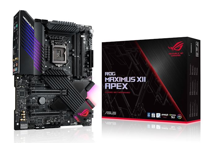
Back in April, Intel released its Z490 chipset for its 10th generation Comet Lake processors with a choice of over 44 models for users to select from. One of the more enthusiast-level models for Z490 was announced by ASUS via its ROG Maximus Apex, with solid overclocking focused traits, but equally with enough features for performance users and gamers too. ASUS has announced that the ROG Maximus Apex is now available to purchase with some of the most prominent features including three PCIe 3.0 x4 M.2 slots, a 16-phase power delivery, an Intel 2.5 GbE Ethernet controller and an Intel Wi-Fi 6 wireless interface.


Not all motherboards are created equal, and not all conform to fit a specific purpose e.g content creation, gaming, or workstation. One of ASUS’s most distinguished brands is the Republic of Gamers series, with its blend of premium controllers, aesthetics, and the models are generally full of features. The Apex series is the brands overclocking focused models, and there have been some fantastic Apex models across the chipsets. ASUS has just put the new ROG Maximus XII Apex into North American retail channels.


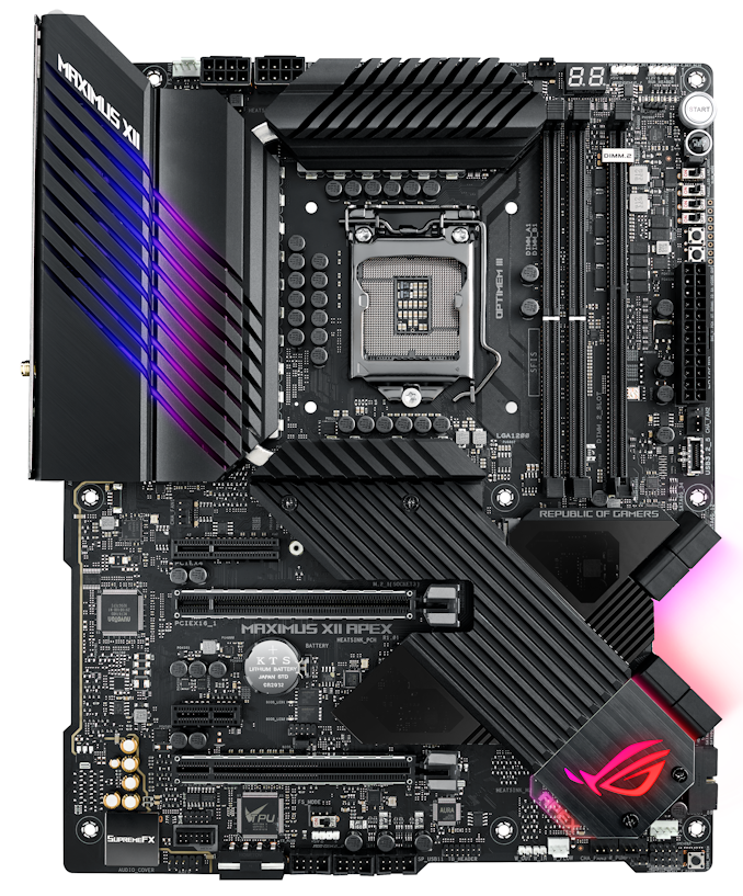
Some of the most notable features of the ASUS ROG Maximus XII Apex include support for up to three PCIe 3.0 x4 M.2 drives, with the use of an included ROG DIMM.2 module included in the accessories bundle. Looking at storage, the Apex includes eight SATA ports which use a friendly V-shaped design to allow easier installation of SATA drives. Despite this board being ATX, ASUS includes just two memory slots with support for up to 64 GB of DDR4-4800 memory, which is likely to improve latencies and overall memory performance when overclocking memory. There are two full-length PCIe 3.0 slots which operate at x16 and x8/x8, with a half-length PCIe 3.0 x4 slot and a single PCIe 3.0 x1 slot. On the rear panel are a load of USB connectivity with four USB 3.2 G2 Type-A, one USB 3.2 G2 Type-C, and five USB 3.2 G1 Type-A ports. For networking, ASUS includes an Intel I225-V 2.5 GbE ethernet controller and an Intel AX201 Wi-Fi 6 interface which also includes support for BT 5.1 devices. The board also includes a SupremeFX S1220A HD codec which adds five 3.5 mm audio jacks and a single S/PDIF optical output on the rear.


Underneath the large power delivery heatsink is a big 16-phase setup with sixteen TDA21490 90 A power stages, with an ASP1405I PWM controller operating in 7+1 mode. This is due to ASUS opting to use teamed power stages with fourteen for the CPU, and two for the SoC, with teamed designed to improve transient response when compared to setups that use doublers. Providing power to the CPU is a pair of 12 V ATX CPU power inputs, while a 4-pin Molex is present to provide additional power to the PCIe slots. 


The ASUS ROG Maximus XII Apex is currently available to purchase at Digital Storm and Cyberpower in the US, with stock expected to land at both Amazon and Newegg very soon. Stockists and retailers such as Scan Computers in the UK also have stock at present.


Related Reading


Source: AnandTech – ASUS ROG Maximus XII Apex Now Available

Qualcomm Announces New Snapdragon Wear 4100 & 4100+: 12nm A53 Smartwatches

Today Qualcomm is making a big step forward in its smartwatch SoC offerings by introducing the brand-new Snapdragon Wear 4100 and Wear 4100+ platforms. The new chips succeed the aging two 2018 originating Wear 3100 platforms and significantly upgrading the hardware specifications, bringing to the table all new IPs for CPU, GPU and DSPs, all manufactured on a newer lower power process node.


Source: AnandTech – Qualcomm Announces New Snapdragon Wear 4100 & 4100+: 12nm A53 Smartwatches

AMD Publishes First Beta Driver With Windows 10 Hardware GPU Scheduling Support

Following last week’s release of NVIDIA’s first Hardware-Accelerated GPU Scheduling-enabled video card driver, AMD this week has stepped up to the plate to do the same. The Radeon Software Adrenalin 2020 Edition 20.5.1 Beta with Graphics Hardware Scheduling driver (version 20.10.17.04) has been posted to AMD’s website, and as the name says on the tin, the driver offers support for Windows 10’s new hardware-accelerated GPU scheduling technology.


As a quick refresher, hardware acceleration for GPU scheduling was added to the Windows display driver stack with WDDM 2.7 (shipping in Win10 2004). And, as alluded to by the name, it allows GPUs to more directly manage their VRAM. Traditionally Windows itself has done a lot of the VRAM management for GPUs, so this is a distinctive change in matters.


Microsoft has been treating the feature as a relatively low-key development – relative to DirectX 12 Ultimate, they haven’t said a whole lot about it – meanwhile AMD’s release notes make vague performance improvement claims, stating “By moving scheduling responsibilities from software into hardware, this feature has the potential to improve GPU responsiveness and to allow additional innovation in GPU workload management in the future”. As was the case with NVIDIA’s release last week, don’t expect anything too significant here, otherwise AMD would be more heavily promoting the performance gains. But it’s something to keep an eye on over the long term.


In the meantime, AMD seems to be taking a cautious approach here. The beta driver has been published outside their normal release channels and only supports products using AMD’s Navi 10 GPUs – so the Radeon 5700 series, 5600 series, and their mobile variants. Support for the Navi 14-based 5500 series is notably absent, as is Vega support for both discrete and integrated GPUs.


Additional details about the driver release, as well as download instructions, can be found on AMD’s website in the driver release notes.


Finally, on a tangential note, I’m aiming to sit down with The Powers That Be over the next week or so in order to better dig into hardware-accelerated GPU scheduling. Since it’s mostly a hardware developer-focused feature, Microsoft hasn’t talked about it much in the consumer context or with press. So I’ll be diving into more on the theory behind it: what it’s meant to do, future feature prospects, and as well as the rationale for introducing it now as opposed to earlier (or later). Be sure to check back in next week for that.


Source: AnandTech – AMD Publishes First Beta Driver With Windows 10 Hardware GPU Scheduling Support

The OnePlus 8, OnePlus 8 Pro Pro Review: Becoming The Flagship

It’s been a couple of months since OnePlus released the new OnePlus 8 & OnePlus 8 Pro, and both devices have received plenty of software updates improving the device’s experiences and camera qualities. Today, it’s time to finally go over the full review of both devices, which OnePlus no longer really calls “flagship killers”, but rather outright flagships.


The OnePlus 8, and especially the OnePlus 8 pro are big step-up redesigns from the company, significantly raising the bar in regards to the specifications and features of the phones. The OnePlus 8 Pro is essentially a check-marked wish-list of characteristics that were missing from last year’s OnePlus 7 Pro as the company has addressed some of its predecessors’ biggest criticisms. The slightly smaller and cheaper regular OnePlus 8 more closely follows its predecessors’ ethos as well as competitive pricing, all whilst adopting the new design language that’s been updated with this year’s devices.


Source: AnandTech – The OnePlus 8, OnePlus 8 Pro Pro Review: Becoming The Flagship

HPC Systems Special Offer: Two A64FX Nodes in a 2U for $40k

It was recently announced that the Fugaku supercomputer, located at Riken in Japan, has scored the #1 position on the TOP500 supercomputer list, as well as #1 positions in a number of key supercomputer benchmarks. At the heart of Fugaku isn’t any standard x86 processor, but one based on Arm – specifically, the A64FX 48+4-core processor, which uses Arm’s Scalable Vector Extensions (SVE) to enable high-throughput FP64 compute. At 435 PetaFLOPs and 7.3 million cores, Fugaku beat the former #1 system by 2.8x in performance. Currently Fugaku has been used for COVID-19 related research, such as modelling tracking rates or virus in liquid droplet dispersion.


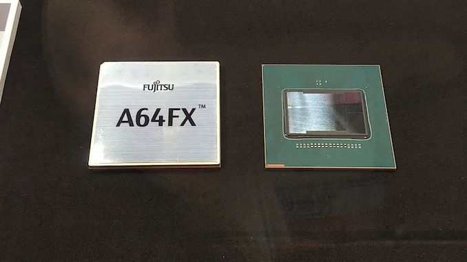
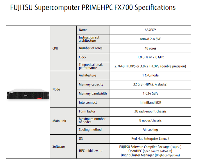
The Fujitsu A64FX card is a unique piece of kit, offering 48 compute cores and 4 control cores, each with monumental bandwidth to keep the 512-bit wide SVE units fed. The chip runs at 2.2 GHz, and can operate in FP64, FP32, FP16 and INT8 modes for a variety of AI applications. There is 1 TB/sec of bandwidth from the 32 GB of HBM2 on each card, and because there are four control cores per chip, it runs by itself without any external host/device situation.


It wasn’t ever clear if the A64FX module would be available on a wider scale beyond supercomputer sales, however today confirms that it is, with the Japanese based HPC Systems set to offer a Fujitsu PrimeHPC FX700 server that contains up to eight A64FX nodes (at 1.8 GHz) within a 2U form factor. Each note is paired with 512 GB of SSD storage and gigabit Ethernet capabilities, with room for expansion (Infiniband EDR etc). The current deal at HPC Systems is for a 2-node implementation, at a price of ¥4,155,330 (~$39000 USD), with the deal running to the end of the year.


The A64FX card already has listed support for quantum chemical calculation software Gaussian16, molecular dynamics software AMBER, non-linear structure analysis software LS-DYNA. Other commercial packages in the structure and fluid analysis fields will be coming on board in due course. There is also Fujitsu’s Software Compiler Package v1.0 to enable developers to build their own software.


Source: HPC Systems, PDF Flyer


Related Reading


Source: AnandTech – HPC Systems Special Offer: Two A64FX Nodes in a 2U for k

Sponsored Post: Check Out all of the ASUS B550 Motherboards Available Now

The arrival of the AMD B550 chipset is an exciting prospect for PC builders, as it’s the first to bring the potential of PCIe 4.0 to the forefront for mainstream builders. ASUS has a diverse selection of new motherboards to choose from with this chipset, and this useful B550 motherboard guide will help you figure out which one is right for you.

In ASUS B550 motherboards, the main PCIe x16 and M.2 slots are PCIe 4.0-capable. They also feature up to four USB 3.2 Gen 2 ports that clock in with a maximum supported speed of 10Gbps each. The chipset’s built-in lanes now have PCIe 3.0 connectivity as well, which is great to see. Additionally, AMD has noted that future CPUs built on the Zen 3 architecture will be fully compatible with B550 motherboards, making them a safe and long-lasting investment for people who wish to upgrade to those new processors down the line.


Source: AnandTech – Sponsored Post: Check Out all of the ASUS B550 Motherboards Available Now

Intel’s Raja Koduri Teases “Ponte Vecchio” Xe GPU Silicon

Absent from the discrete GPU space for over 20 years, this year Intel is set to see the first fruits from their labors to re-enter that market. The company has been developing their new Xe family of GPUs for a few years now, and the first products are finally set to arrive in the coming months with the Xe-LP-based DG1 discrete GPU, as well as Tiger Lake’s integrated GPU, kicking off the Xe GPU era for Intel.


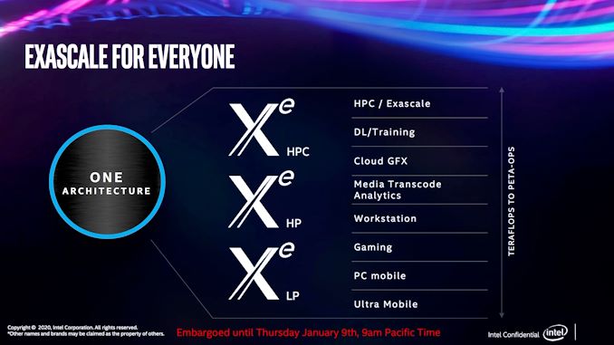
But those first Xe-LP products are just the tip of a much larger iceberg. Intending to develop a comprehensive top-to-bottom GPU product stack, Intel is also working on GPUs optimized for the high-power discrete market (Xe-HP), as well as the high-performance computing market (Xe-HPC).


Xe-HPC, in turn, is arguably the most important of the three segments for Intel, as well as being the riskiest. The server-class GPU will be responsible for broadening Intel’s lucrative server business beyond CPUs, along with fending off NVIDIA and other GPU/accelerator rivals, who in the last few years have ridden the deep learning wave to booming profits and market shares that increasingly threaten Intel’s traditional market dominance. The server market is also the riskiest market, due to the high-stakes nature of the hardware: the only thing bigger than the profits are the chips, and thus the costs to enter the market. So under the watchful eye of Raja Koduri, Intel’s GPU guru, the company is gearing up to stage a major assault into the GPU space.


That brings us to the matter of this week’s teaser. One of the benefits of being a (relatively) upstart rival in the GPU business is that Intel doesn’t have any current-generation products that they need to protect; without the risk of Osborning themselves, they’re free to talk about their upcoming products even well before they ship. So, as a bit of a savvy social media ham, Koduri has been posting occasional photos of Ponte Vecchio, the first Xe-HPC GPU, as Intel brings it up in their labs.


Today’s teaser from Koduri shows off a tray with three different Ponte Vecchio chips of different sizes. While detailed information about Ponte Vecchio is still limited, Intel has previously commented that Ponte Vecchio would be taking a chiplet route for the GPU, using multiple chiplets to build larger and more powerful designs. Koduri’s latest photo, in turn, looks to be a clear illustration of that, with the larger chip sizes roughly correlating to 1×2 and 2×2 configurations of the smallest chip.


And with presumably multiple chiplets under the hood, the resulting chips are quite sizable. With a helpful 18650 battery in the photo for reference, we can see that the smaller packages are around 65mm wide, while the largest package is easily approaching 110mm on a side.  (For refence, an Intel desktop CPU is around 37.5mm x 37.5mm).


Finally, in a separate tweet, Koduri quickly talks about performance: “And..they let me hold peta ops in my palm(almost:)!” Koduri doesn’t go into any detail about the numeric format involved – an important qualifier when talking about compute throughput on GPUs that can process lower-precision formats at higher rates – but we’ll be generous and assume INT8 operations. INT8 has become a fairly popular format for deep learning inference, as the integer format offers great performance for neural nets that don’t need high precision. NVIDIA’s A100 accelerator, for reference, tops out at 0.624 PetaOPs for regular tensor operations, or 1.248 PetaOps for a sparse matrix.


And that is the latest on Ponte Vecchio. Though with the parts likely not shipping until later in 2021 as part of the Aurora supercomputer, it’s likely not going to be the last word from Intel and Koduri on their first family of HPC GPUs.


Source: AnandTech – Intel’s Raja Koduri Teases “Ponte Vecchio” Xe GPU Silicon

Intel’s Raja Koduri Teases Even Larger Xe GPU Silicon

Absent from the discrete GPU space for over 20 years, this year Intel is set to see the first fruits from their labors to re-enter that market. The company has been developing their new Xe family of GPUs for a few years now, and the first products are finally set to arrive in the coming months with the Xe-LP-based DG1 discrete GPU, as well as Tiger Lake’s integrated GPU, kicking off the Xe GPU era for Intel.


But those first Xe-LP products are just the tip of a much larger iceberg. Intending to develop a comprehensive top-to-bottom GPU product stack, Intel is also working on GPUs optimized for the high-power discrete market (Xe-HP), as well as the high-performance computing market (Xe-HPC).


That high end of the market, in turn, is arguably the most important of the three segments for Intel, as well as being the riskiest. The server-class GPUs will be responsible for broadening Intel’s lucrative server business beyond CPUs, along with fending off NVIDIA and other GPU/accelerator rivals, who in the last few years have ridden the deep learning wave to booming profits and market shares that increasingly threaten Intel’s traditional market dominance. The server market is also the riskiest market, due to the high-stakes nature of the hardware: the only thing bigger than the profits are the chips, and thus the costs to enter the market. So under the watchful eye of Raja Koduri, Intel’s GPU guru, the company is gearing up to stage a major assault into the GPU space.


That brings us to the matter of this week’s teaser. One of the benefits of being a (relatively) upstart rival in the GPU business is that Intel doesn’t have any current-generation products that they need to protect; without the risk of Osborning themselves, they’re free to talk about their upcoming products even well before they ship. So, as a bit of a savvy social media ham, Koduri has been posting occasional photos of Intel’s Xe GPUs, as Intel brings them up in their labs.


Today’s teaser from Koduri shows off a tray with three different Xe chips of different sizes. While detailed information about the Xe family is still limited, Intel has previously commented that the Xe-HPC-based Ponte Vecchio would be taking a chiplet route for the GPU, using multiple chiplets to build larger and more powerful designs. So while Koduri’s tweets don’t make it clear what specific GPUs we’re looking at – if they’re all part of the Xe-HP family or a mix of different families – the photo is an interesting hint that Intel may be looking at a wider use of chiplets, as the larger chip sizes roughly correlate to 1×2 and 2×2 configurations of the smallest chip.


And with presumably multiple chiplets under the hood, the resulting chips are quite sizable. With a helpful AA battery in the photo for reference, we can see that the smaller packages are around 50mm wide, while the largest package is easily approaching 85mm on a side.  (For refence, an Intel desktop CPU is around 37.5mm x 37.5mm).


Finally, in a separate tweet, Koduri quickly talks about performance: “And..they let me hold peta ops in my palm(almost:)!” Koduri doesn’t go into any detail about the numeric format involved – an important qualifier when talking about compute throughput on GPUs that can process lower-precision formats at higher rates – but we’ll be generous and assume INT8 operations. INT8 has become a fairly popular format for deep learning inference, as the integer format offers great performance for neural nets that don’t need high precision. NVIDIA’s A100 accelerator, for reference, tops out at 0.624 PetaOPs for regular tensor operations, or 1.248 PetaOps for a sparse matrix.


And that is the latest on Xe. With the higher-end discrete parts likely not shipping until later in 2021, this is likely not going to be the last word from Intel and Koduri on their first modern family of discrete GPUs.


Update: A previous version of the article called the large chip Ponte Vecchio, Intel’s Xe-HPC flagship. We have since come to understand that the silicon we’re seeing is likely not Ponte Vecchio, making it likely to be something Xe-HP based


Source: AnandTech – Intel’s Raja Koduri Teases Even Larger Xe GPU Silicon

AMD Succeeds in its 25×20 Goal: Renoir Crosses the Line in 2020

One of the stories bubbling away in the background of the industry is the AMD self-imposed ‘25×20’ goal. Starting with performance in 2014, AMD committed to itself, to customers, and to investors that it would achieve an overall 25x improvement in ‘Performance Efficiency’ by 2020, which is a function of raw performance and power consumption. At the time AMD was defining its Kaveri mobile product as the baseline for the challenge – admittedly a very low bar – however each year AMD has updated us on its progress. With this year being 2020, the question on my lips ever since the launch of Zen2 for mobile was if AMD had achieved its goal, and if so, by how much? The answer is yes, and by a lot.

In this article we will recap the 25×20 project, how the metrics are calculated, and what this means for AMD in the long term.


Source: AnandTech – AMD Succeeds in its 25×20 Goal: Renoir Crosses the Line in 2020

NVIDIA Posts First DirectX 12 Ultimate Driver Set, Enables GPU Hardware Scheduling

NVIDIA sends word this morning that the company has posted their first DirectX 12 Ultimate-compliant driver. Published as version 451.48 – the first driver out of NVIDIA’s new Release 450 driver branch – the new driver is the first release from the company to explicitly support the latest iteration of DirectX 12, enabling support for features such as DXR 1.1 ray tracing and tier 2 variable rate shading. As well, this driver also enables support for hardware accelerated GPU scheduling.


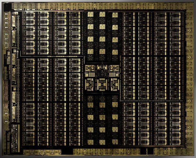
As a quick refresher, DirectX 12 Ultimate is Microsoft’s latest iteration of the DirectX 12 graphics API, with Microsoft using it to synchronize the state of the API between current-generation PCs and the forthcoming Xbox Series X console, as well as to set a well-defined feature baseline for future game development. Based around the capabilities of current generation GPUs (namely: NVIDIA Turing) and the Xbox Series X’s AMD RDNA2-derrived GPU, DirectX 12 Ultimate introduces several new GPU features under a new feature tier (12_2). This includes an updated version of DirectX’s ray tracing API, DXR 1.1, as well as tier 2 variable rate shading, mesh shaders, and sampler feedback. The software groundwork for this has been laid in the latest version of Windows 10, version 2004, and now is being enabled in GPU drivers for the first time.


DirectX 12 Feature Levels
  12_2

(DX12 Ult.)
12_1 12_0
GPU Architectures

(Introduced as of)
NVIDIA: Turing

AMD: RDNA2

Intel: Xe?
NVIDIA: Maxwell 2

AMD: Vega

Intel: Gen9
NVIDIA: Maxwell 2

AMD: Hawaii

Intel: Gen9
Ray Tracing

(DXR 1.1)
Yes No No
Variable Rate Shading

(Tier 2)
Yes No No
Mesh Shaders Yes No No
Sampler Feedback Yes No No
Conservative Rasterization Yes Yes No
Raster Order Views Yes Yes No
Tiled Resources

(Tier 2)
Yes Yes Yes
Bindless Resources

(Tier 2)
Yes Yes Yes
Typed UAV Load Yes Yes Yes

In the case of NVIDIA’s recent video cards, the underlying Turing architecture has supported these features since the very beginning. However, their use has been partially restricted to games relying on NVIDIA’s proprietary feature extensions, due to a lack of standardized API support. Overall it’s taken most of the last two years to get the complete feature set added to DirectX, and while NVIDIA isn’t hesitating to use this moment to proclaim their GPU superiority as the first vendor to ship DirectX 12 Ultimate support, to some degree it’s definitely vindication of the investment the company put in to baking these features into Turing.


In any case, enabling DirectX 12 Ultimate support is an important step for the company, though one that’s mostly about laying the groundwork for game developers, and ultimately, future games. At this point no previously-announced games have confirmed that they’ll be using DX12U, though this is just a matter of time, especially with the Xbox Series X launching in a few weeks.


Perhaps the more interesting aspect of this driver release, though only tangential to DirectX 12 Ultimate support, is that NVIDIA is enabling support for hardware accelerated GPU scheduling. This mysterious feature was added to the Windows display driver stack with WDDM 2.7 (shipping in Win10 2004), and as alluded to by the name, it allows GPUs to more directly manage their VRAM. Traditionally Windows itself has done a lot of the VRAM management for GPUs, so this is a distinctive change in matters.


At a high level, NVIDIA is claiming that hardware accelerated GPU scheduling should offer minor improvements to the user experience, largely by reducing latency and improving performance thanks to more efficient video memory handling. I would not expect anything too significant here – otherwise NVIDIA would be heavily promoting the performance gains – but it’s something to keep an eye out for. Meanwhile, absent any other details, I find it interesting that NVIDIA lumps video playback in here as a beneficiary as well, since video playback is rarely an issue these days. At any rate, the video memory handling changes are being instituted at a low level, so hardware scheduling is not only for DirectX games and the Windows desktop, but also for Vulkan and OpenGL games as well.


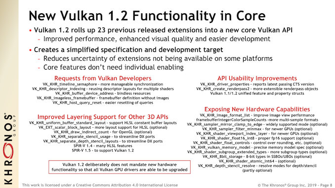
Speaking of Vulkan, the open source API is also getting some attention with this driver release. 451.48 is the first GeForce driver with support for Vulkan 1.2, the latest version of that API. An important housekeeping update for Vulkan, 1.2 is promoting a number of previously optional feature extensions into the core Vulkan API, such as Timeline Semaphores, as well as improved cross portability support by adding full support for HLSL (i.e. DirectX) shaders within Vulkan.


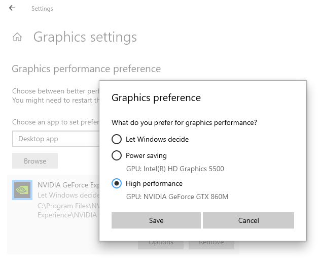
Finally, while tangential to today’s driver release, NVIDIA has posted an interesting note on its customer support portal regarding Windows GPU selection that’s worth making note of. In short, Windows 10 2004 has done away with the “Run with graphics processor” contextual menu option within NVIDIA’s drivers, which prior to now has been a shortcut method of forcing which GPU an application runs on it an Optimus system. In fact, it looks like control over this has been removed from NVIDIA’s drivers entirely. As noted in the support document, controlling which GPU is used is now handled through Windows itself, which means laptop users will need to get used to going into the Windows Settings panel to make any changes.


As always, you can find the full details on NVIDIA’s new GeForce driver, as well as the associated release notes, over on NVIDIA’s driver download page.


Source: AnandTech – NVIDIA Posts First DirectX 12 Ultimate Driver Set, Enables GPU Hardware Scheduling

Western Digital Announces Ultrastar DC SN840 Dual-Port NVMe SSD

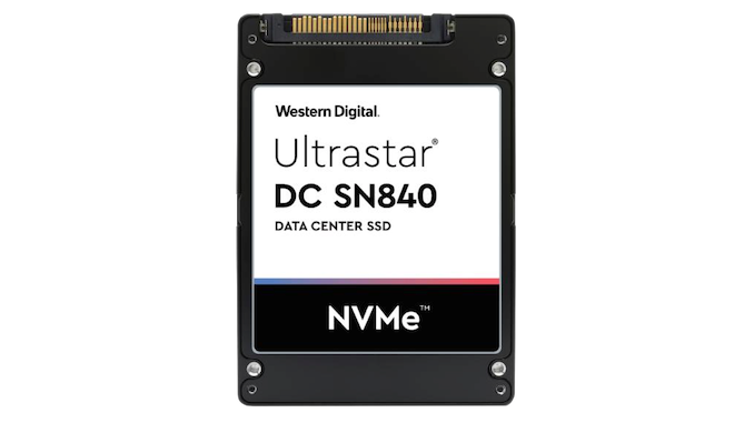
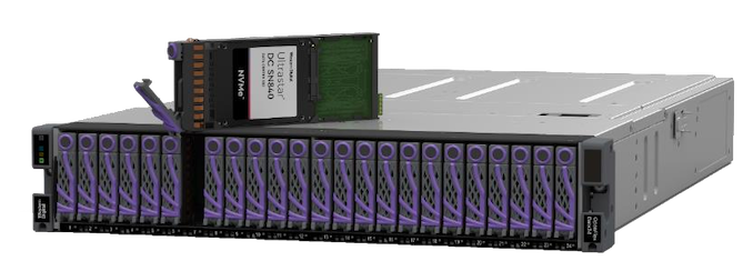
Western Digital is introducing a new high-end enterprise NVMe SSD, the Ultrastar DC SN840, and a NVMe over Fabrics 2U JBOF using up to 24 of these SSDs.


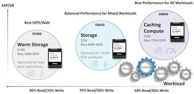
The Ultrastar DC SN840 uses the same 96L TLC and in-house SSD controller as the SN640, but the SN840 offers more features, performance and endurance to serve a higher market segment than the more mainstream SN640. The SN840 uses a 15mm thick U.2 form factor compared to 7mm U.2 (and M.2 and EDSFF options) for the SN640, which allows the SN840 to handle much higher power levels and to accommodate higher drive capacities in the U.2 form factor. The controller is still a PCIe 3 design so peak sequential read performance is barely faster than the SN640, but the rest of the performance metrics are much faster than the SN640: random reads now saturate the PCIe 3 x4 link and write performance is much higher across the board. Power consumption can reach 25W, but the SN840 provides a range of configurable power states to limit it to as little as 11W.


Western Digital Ultrastar DC

Enterprise NVMe SSD Specifications
  Ultrastar DC SN840 Ultrastar DC SN640

(U.2 variant)
Ultrastar DC SN340
Form Factor 2.5″ 15mm U.2 2.5″ 7mm U.2 2.5″ 7mm U.2
Interface PCIe 3 x4

or x2+x2 dual-port
PCIe 3 x4 PCIe 3 x4
NAND Flash Western Digital 96L BiCS4 3D TLC
Capacities
1.92 TB

3.84 TB

7.68 TB

15.36 TB

1.6 TB

3.2 TB

6.4 TB
960 GB

1.92 TB

3.84 TB

7.68 TB
800 GB

1.6 TB

3.2 TB

6.4 TB


3.84 TB

7.68 TB

Write Endurance 1 DWPD 3 DWPD 0.8 DWPD 2 DWPD 0.3 DWPD
Sequential Read 3.3 GB/s 3.1 GB/s 3.1 GB/s
Sequential Write 3.1 GB/s 3.2 GB/s 2 GB/s 1.4 GB/s
Random Read IOPS 780k 472k 473k 429k
Random Write IOPS 160k 257k 65k 116k 7k (32kB writes)
Random 70/30 Mixed IOPS 401k 503k 194k 307k 139k (32kB writes)
Active Power 25 W 12 W 6.5 W
Warranty 5 years

The SN840 supports dual-port PCIe operation for high availability, a standard feature for SAS drives but usually only found on enterprise NVMe SSDs that are top of the line or special-purpose models. Other enterprise-oriented features include optional self-encrypting drive capability and support for configuring up to 128 NVMe namespaces.


The SN840 will be available in two endurance tiers, rated for 1 drive write per day (DWPD) and 3 DWPD—fairly standard, but a step up from the 0.8 DWPD and 2 DWPD tiers offered by the SN640. The high-endurance tier will offer capacities from 1.6 TB to 6.4 TB, while the lower-endurance tier has slightly higher usable capacities at each level, and adds a 15.36 TB capacity at the top. (The SN640 is due to get a 15.36 TB option in the EDSFF form factor only.)


Between the SN840, SN640 and SN340, Western Digital’s enterprise NVMe SSDs now cover a wide range of use cases, all with their latest 96L 3D TLC NAND and in-house controller designs. Shipments of the SN840 begin in July.


OpenFlex Data24 NVMe Over Fabrics JBOF


Using the new Ultrastar DC SN840 drives, Western Digital is also introducing a new product to its OpenFlex family of NVMe over Fabrics products. The OpenFlex Data24 is a fairly simple Ethernet-attached 2U JBOF enclosure supporting up to 24 SSDs (368TB total). These drives are connected through a PCIe switch fabric to up to six ports of 100Gb Ethernet, provided by RapidFlex NVMeoF controllers that were developed by recent WDC acquisition Kazan Networks. The OpenFlex Data24 is a much more standard-looking JBOF design than the existing 3U OpenFlex F3100 that packs its storage in 10 modules with a proprietary form factor; the Data24 also has a shorter depth to fit into more common rack sizes. The OpenFlex Data24 will also be slightly cheaper and much faster than their Ultrastar 2U24 SAS JBOF solution.


The OpenFlex Data24 will launch this fall.


Related Reading


Source: AnandTech – Western Digital Announces Ultrastar DC SN840 Dual-Port NVMe SSD

The Intel W480 Motherboard Overview: LGA1200 For Xeon W-1200

During Intel’s unveiling of the Z490 chipset and Intel Core 10th generation Comet Lake processors, Intel also announced its series of Xeon W-1200 processors. To accompany this announcement, without much fanfare, Intel also launched the W480 chipset which also features an LGA1200 socket. Aiming for a more professional feel for processors with ECC support, vendors have announced a variety of W480 models. Some target content creators, and others for workstation environments. These boards are paired solely with W-1200, and support both ECC and non-ECC DDR4 memory.


Source: AnandTech – The Intel W480 Motherboard Overview: LGA1200 For Xeon W-1200

Western Digital Announces Red Pro Plus HDDs, Cleans Up Red SMR Mess with Plus Branding

Western Digital originally launched their Red lineup of hard disk drives for network-attached storage devices back in 2012. The product stack later expanded to service professional NAS units with the Red Pro. These drives have traditionally offered very predictable performance characteristics, thanks to the use of conventional magnetic recording (CMR). More recently, with the advent of shingled magnetic recording (SMR), WD began offering drive-managed versions in the direct-attached storage (DAS) space for consumers, and host-managed versions for datacenters.


Towards the middle of 2019, WD silently introduced WD Red hard drives (2-6TB capacities) based on drive-managed SMR. There was no fanfare or press-release, and the appearance of the drives in the market was not noticed by the tech press. Almost a year after the drives appeared on the shelves, the voice of customers dissatisfied with the performance of the SMR drives in their NAS units reached levels that WD could no longer ignore. In fact, as soon as we heard about the widespread usage of SMR in certain WD Red capacities, we took those drives off our recommended HDDs list.


Finally, after starting to make amends towards the end of April 2020, Western Digital has gone one step further at last, and cleaned up their NAS drive branding to make it clear which drives are SMR-based. Re-organizing their Red portfolio, the vanilla WD Red family has become a pure SMR lineup. Meanwhile a new brand, the Red Plus, will encompass the 5400 RPM CMR hard drives that the WD Red brand was previously known for. Finally, the Red Pro lineup remains unchanged, with 7200 RPM CMR drives for high performance configurations.


WD NAS Hard Drives for Consumer / SOHO / SMB Systems (Source: Western Digital Blog)


While Western Digital (and consumers) should have never ended up in this situation in the first place, it’s nonetheless an important change to WD’s lineup that restores some badly-needed clarity to their product lines. The technical and performance differences between CMR and SMR drives are significant, and having the two used interchangeably in the Red line – in a lineup that previously didn’t contain any SMR drives to begin with – was always going to be a problem.


In particular, a look at various threads in NAS forums indicates that most customers of these SMR Red drives faced problems with certain RAID and ZFS operations. The typical consumer use-case for NAS drives – even just 1-8 bays – may include RAID rebuilds, RAID expansions, and regular scrubbing operations. The nature of drive-managed SMR makes it unsuitable for those types of configurations.


It was also not clear what WD hoped to achieve by using SMR for lower-capacity drives. Certain capacity points, such as the 2TB and 4TB, have one less platter in the SMR version compared to the CMR, which should result in lowered production costs. But the trade-offs associated with harming drive performance in certain NAS configurations – and subsequently ruining the reputation of Red drives in the minds of consumers – should have been considered.


In any case, it seems probable that the lower-capacity SMR WD Red drives were launched more as a beta test for the eventual launch of SMR-based high-capacity drives. Perhaps, the launch of these drives under a different branding – say, Red Archive, instead of polluting the WD Red branding, would have been better from a marketing perspective.


As SMR became entrenched in the consumer space, it was perhaps inevitable that NAS drives utilizing the technology would appear in the market. However in the process, WD has missed a golden chance to educate consumers on situations where SMR drives make sense in NAS units.


For our part, while the updated branding situation is a significant improvement, we do not completely agree with WD’s claim about SMR Reds being suitable for SOHO NAS units. This may lead to non-tech savvy consumers using them in RAID configurations, even in commercial off-the-shelf (COTS) NAS units such as those from QNAP and Synology. Our recommendation is to use these SMR Reds for archival purposes (an alternative to tape backups for the home – not that consumers are doing tape backups today!), or, in WORM (Write-Once Read-Many) scenarios in a parity-less configuration such as RAID1 or RAID10. It is not advisable to subject these drives to RAID rebuilds or scrubbing operations, and ZFS is not even in the picture. The upside, at least, is that in most cases users contemplating ZFS are tech-savvy enough to know the pitfalls of SMR for their application.


All said, WD has one of the better implementations of SMR (in the DAS space), as we wrote earlier. But that is for direct-attached storage, which gives SMR drives plenty of time to address the ‘garbage-collection’ needs. It is just that consumer NAS behavior (that is not explicitly user-triggered) may not be similar to that.


Consumers considering the WD Red lineup prior to the SMR fiasco can now focus on the Red Plus drives. We do not advise consumers to buy the vanilla Red (SMR) unless they are aware of what they are signing up for. To this effect, consumers need to become well-educated regarding the use-cases for such drives. Seagate’s 8TB Archive HDD was launched in 2015, but didn’t meet with much success in the consumer market for that very reason (and had to be repurposed for DAS applications). The HDD vendors’ marketing teams have their task cut out if high-capacity SMR drives for consumer NAS systems are in their product roadmap.


Source: AnandTech – Western Digital Announces Red Pro Plus HDDs, Cleans Up Red SMR Mess with Plus Branding

Marvell’s ThunderX3 Server Team Loses VP/GM and Lead Architect

One of the key drivers in the Arm server space over the last few years has been the cohesion of the different product teams attempting to build the next processor to attack the dominance of x86 in the enterprise market. A number of companies and products have come and gone (Qualcomm’s Centriq) or been acquired (Annapurna by Amazon, Applied Micro by Ampere), with varying degrees of success, some of which is linked to the key personnel in each team. One of our readers has recently highlighted us to a recent movement in this space: Gopal Hegde, the VP/GM of the ThunderX Processor Business Unit at Marvell, has now left the company.


Source: AnandTech – Marvell’s ThunderX3 Server Team Loses VP/GM and Lead Architect

Acer Updates The Compact Juggernaut: Predator Orion 3000 Hands-On

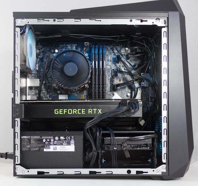
Today at the Next@Acer conference, Acer is announcing an updated version of their compact gaming desktop, the Predator Orion 3000, and the company was able to send us a pre-production unit for a hands-on. As this is a pre-production unit, final performance is not yet fine-tuned, but we can go over the new chassis design, as well as the internals of this mid-sized tower PC.


Acer Predator Desktop
  Orion 3000
CPU 10th Generation Intel Core i5 Processor


10th Generation Intel Core i7 Processor

GPU NVIDIA GeForce GTX Options:

GTX 1650

GTX 1660


NVIDIA RTX Options:

RTX 2060

RTX 2060 Super

RTX 2070 Super

RAM Up to 64 GB DDR4-2666
Storage PCIe NVMe Options:

128 GB / 256 GB / 512 GB / 1 TB M.2 2280


2 x 3.5-inch SATA bays

Up to 2 x 3 TB HDD

Networking Killer E2600 Gigabit Ethernet

Wi-Fi 6

Bluetooth 5.1
Cooling Dual Predator Frostblade RGB fans
I/O – Rear 4 x USB 3.2

2 x USB 2.0

3.5 mm audio
I/O – Front 1 x USB Type-A

1 x USB Type-C

3.5mm audio
Dimensions 15.4 x 6.8 x 10.5 inches (HxWxD)
Starting Price $999.99
Availability September 2020

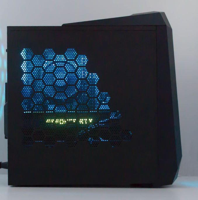
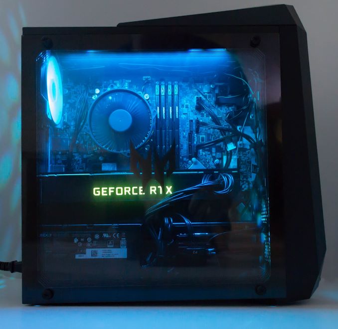
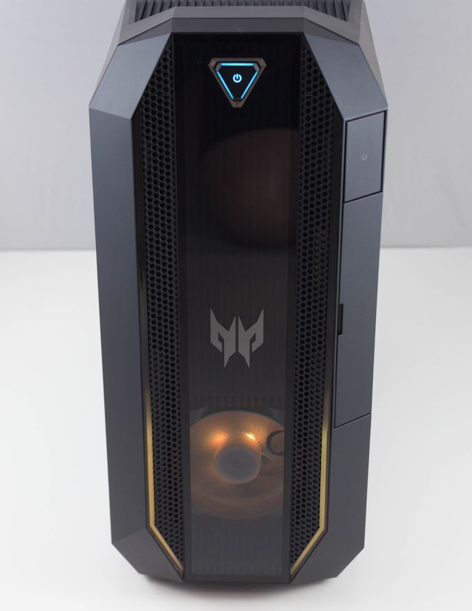
Acer’s updated Orion 3000 chassis is a well-thought out design, with some excellent features, and a compact and stylish design that would fit well on any gaming desk. Acer offers the Orion 3000 with a black perforated side panel, or you can opt for an EMI compliant tempered glass side if you want to check out the RGB-lit interior. At 18 Liters, the Orion 3000 is also surprisingly compact considering the powerful components inside.


Keeping everything cool are two Predator “Frostblade” fans, with 16.7 million colors to choose from in the PredatorSense App. The RGB also continues with two accent lights along the front of the case, and with or without the clear side panel, the lighting is plenty to create a glow around the system. Powering up the system was impressive, not only because of the random RGB color scheme, but also because the Frostblade fans were tuned for a very low noise level. The system, even as a pre-production sample, was nearly silent at idle.


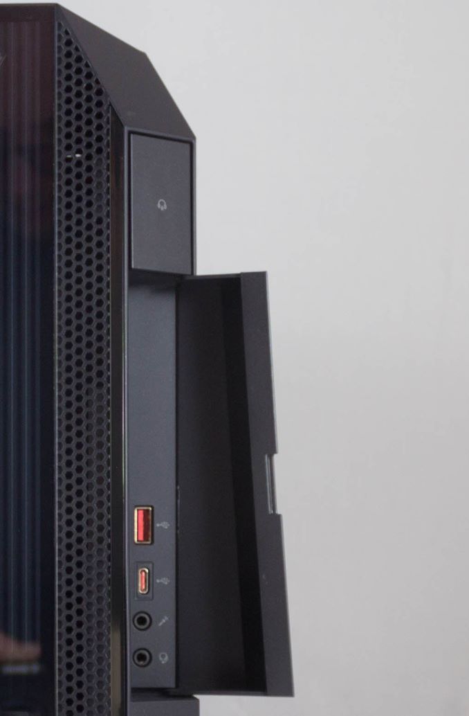
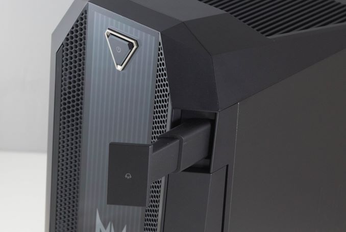
The Orion 3000 isn’t just about style though. Acer has some wonderful functional elements to their design as well. The top of the case houses a built-in carrying handle, which makes the small desktop very easy to move around, and although I am not sure if Acer came up with the idea of including a headset holder built into the chassis, but it’s a brilliant idea and one I wish my own case offered. The power button is very prominent and easy to access, and for the new design Acer has moved the front panel ports behind a small door to keep them concealed when not in use. Whether or not you’d like them behind a door probably depends on how often you use them, but the door looks like it could be removed without too much effort.


As this is a pre-production unit, the cable management will likely be adjusted somewhat in the next couple of months, but even so it did not impede airflow at all.


The case has room for two 3.5-inch SATA drives, as well as an NVMe slot for the built-in storage, of which Acer is offering up to 1 TB for the boot drive. The system will have a single PCIe x16 slot for the GPU, so any expansion will have to be over USB. There’s onboard Gigabit Ethernet and Wi-Fi 6 to cover any networking needs.


Acer will be offering a wide-range of performance, with Core i5 and Core i7 models, and up to 64 GB of DDR4-2666 memory. On the GPU front, Acer is offering the NVIDIA GeForce GTX 1650 and 1660, and RTX 2060, 2060 Super, and 2070 Super options. The sample we were provided featured a 500-Watt power supply, which should be plenty to handle everything Acer is offering.


The redesigned Predator Orion 3000 will be available in September, starting at $999.99 USD.


Source: AnandTech – Acer Updates The Compact Juggernaut: Predator Orion 3000 Hands-On

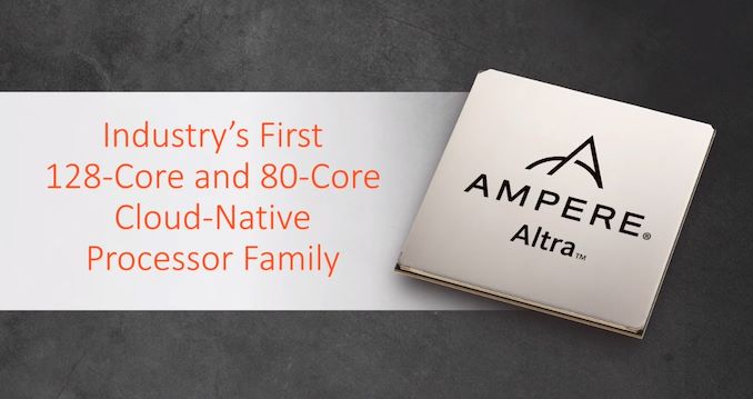
Ampere’s Product List: 80 Cores, up to 3.3 GHz at 250 W; 128 Core in Q4

With the advent of higher performance Arm based cloud computing, a lot of focus is being put on what the various competitors can do in this space. We’ve covered Ampere Computing’s previous eMag products, which actually came from the acquisition of Applied Micro, but the next generation hardware is called Altra, and after a few months of teasing some high performance compute, the company is finally announcing its product list, as well as an upcoming product due for sampling this year.


Source: AnandTech – Ampere’s Product List: 80 Cores, up to 3.3 GHz at 250 W; 128 Core in Q4

The Next Phase: Apple Lays Out Plans To Transition Macs from x86 to Apple SoCs

After many months of rumors and speculation, Apple confirmed this morning during their annual WWDC keynote that the company intends to transition away from using x86 processors at the heart of their Mac family of computers. Replacing the venerable ISA – and the exclusively-Intel chips that Apple has been using – will be Apple’s own Arm-based custom silicon, with the company taking their extensive experience in producing SoCs for iOS devices, and applying that to making SoCs for Macs. With the first consumer devices slated to ship by the end of this year, Apple expects to complete the transition in about two years.


The last (and certainly most anticipated) segment of the keynote, Apple’s announcement that they are moving to using their own SoCs for future Macs was very much a traditional Apple announcement. Which is to say that it offered just enough information to whet developers (and consumers’) appetites without offering too much in the way of details too early. So while Apple has answered some very important questions immediately, there’s also a whole lot more we don’t know at the moment, and likely won’t known until late this year when hardware finally starts shipping.


What we do know, for the moment, is that this is the ultimate power play for Apple, with the company intending to leverage the full benefits of vertical integration. This kind of top-to-bottom control over hardware and software has been a major factor in the success of the company’s iOS devices, both with regards to hard metrics like performance and soft metrics like the user experience. So given what it’s enabled Apple to do for iPhones, iPads, etc, it’s not at all surprising to see that they want to do the same thing for the Mac. Even though the OS itself isn’t changing (much), the ramifications of Apple building the underlying hardware down to the SoC means that they can have the OS make full use of any special features that Apple bakes into their A-series SoCs. Idle power, ISPs, video encode/decode blocks, and neural networking inference are all subjects that are potentially on the table here.


Source: AnandTech – The Next Phase: Apple Lays Out Plans To Transition Macs from x86 to Apple SoCs