The LG V60 and VELVET Review: A Classic & A Design Restart

It’s been a few months since LG has released the LG V60, and since then the company has also finally managed to launch the new Velvet phone to western markets outside of Korea, such as Germany. The two new 2020 phones are quite contrasting devices for LG – representing what one could say the company’s classic design philosophy versus a newer, more refreshing design language. They’re also contrasting devices in terms of their specifications and positioning, with the V60 being a successor flagship devices with a high-end SoC, whilst the new Velvet is a “premium” design with the new Snapdragon 765, coming at a lower price point and some compromises in terms of specification – but not too many as to call it a mid-range phone.


Both phones are overdue a closer look, and that’s precisely what we’ll be doing today.


Source: AnandTech – The LG V60 and VELVET Review: A Classic & A Design Restart

5G in a Fanless Industrial PC from GIGABYTE IPC

One of the key verticals in the integration of 5G we are told is in the industrial space – having machines on a shop floor communicate wireless to a central control hub with ultra-low latency or with ultra-high bandwidth. Automation and control are two elements that these designs can bring, which essentially falls under the ‘Internet of Things’ heading.


To that end, GIGABYTE’s Industrial PC division (GIGAIPC) has developed its first 5G certified PC for industrial use cases. As an added bonus, it is a fanless design, equipped with a Core i3-7100U and with space for up to 32 GB of DDR4. The QBiX Pro (QBiX-Pro-KBLB7100HD-A1) has passed verification field tests with Chunghwa Telecom’s 5G network earlier this year, and comes with a number of key industrial features, such as COM header support, dual Ethernet, video outputs, and plenty of USB. GIGAIPC is aiming its new QBiX Pro at automation, transportation, smart retail, medical, edge computing, and essentially anything IoT that requires high-reliability and 5G connectivity in the field.


5G is provided by an on-board PCIe solution, which GIGAIPC hasn’t cited however we have reached out to get this information. It is very likely to be a combination Qualcomm RF and front-end solution for sub 6 GHz, given the Chunghwa verification, which is attached through an onboard M.2 slot. If previous M.2 solutions are anything to go by, these 5G M.2 modules are wider than the standard M.2 widths we see for storage drives.


Update: It is Qualcomm, however we were not told which one.


Related Reading


Source: AnandTech – 5G in a Fanless Industrial PC from GIGABYTE IPC

DDR5 Memory Specification Released: Setting the Stage for DDR5-6400 And Beyond

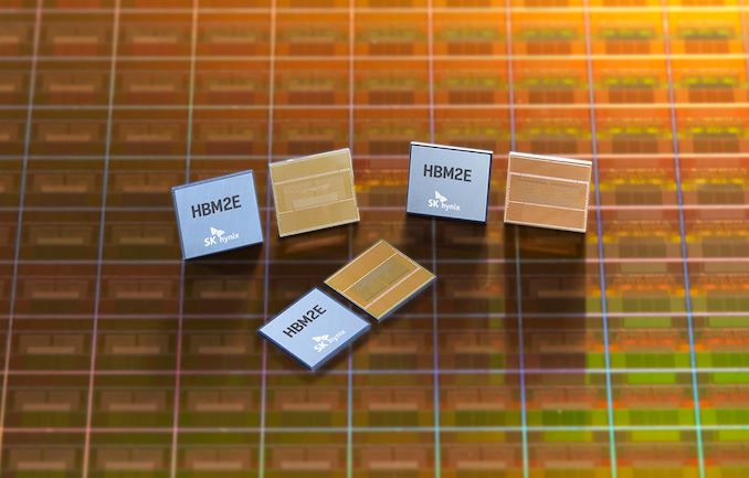
Marking an important milestone in computer memory development, today the JEDEC Solid State Technology Association is releasing the final specification for its next mainstream memory standard, DDR5 SDRAM. The latest iteration of the DDR standard that has been driving PCs, servers, and everything in-between since the late 90s, DDR5 once again extends the capabilities of DDR memory, doubling the peak memory speeds while greatly increasing memory sizes as well. Hardware based on the new standard is expected in 2021, with adoption starting at the sever level before trickling down to client PCs and other devices later on.  


Originally planned for release in 2018, today’s release of the DDR5 specification puts things a bit behind JEDEC’s original schedule, but it doesn’t diminish the importance of the new memory specification. Like every iteration of DDR before it, the primary focus for DDR5 is once again on improving memory density as well as speeds. JEDEC is looking to double both, with maximum memory speeds set to reach at least 6.4Gbps while the capacity for a single, packed-to-the-rafters LRDIMM will eventually be able to reach 2TB. All the while, there are several smaller changes to either support these goals or to simplify certain aspects of the ecosystem, such as on-DIMM voltage regulators as well as on-die ECC.


JEDEC DDR Generations
  DDR5 DDR4 DDR3 LPDDR5
Max Die Density 64 Gbit 16 Gbit 4 Gbit 32 Gbit
Max UDIMM Size 128 GB 32 GB 8 GB N/A
Max Data Rate 6.4 Gbps 3.2 Gbps 1.6 Gbps 6.4Gbps
Channels 2 1 1 1
Width (Non-ECC) 64-bits (2×32) 64-bits 64-bits 16-bits
Banks

(Per Group)
4 4 8 16
Bank Groups 8/4 4/2 1 4
Burst Length BL16 BL8 BL8 BL16
Voltage (Vdd) 1.1v 1.2v 1.5v 1.05v
Vddq 1.1v 1.2v 1.5v 0.5v

Going Bigger: Denser Memory & Die-Stacking


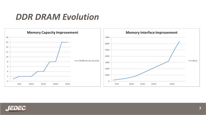
We’ll start with a brief look at capacity and density, as this is the most-straightforward change to the standard compared to DDR4. Designed to span several years (if not longer), DDR5 will allow for individual memory chips up to 64Gbit in density, which is 4x higher than DDR4’s 16Gbit density maximum. Combined with die stacking, which allows for up to 8 dies to be stacked as a single chip, then a 40 element LRDIMM can reach an effective memory capacity of 2TB. Or for the more humble unbuffered DIMM, this would mean we’ll eventually see DIMM capacities reach 128GB for your typical dual rank configuration.


Of course, the DDR5 specification’s peak capacities are meant for later in the standard’s lifetime, when chip manufacturing catches up to what the spec can allow. To start things off memory manufacturers will be using today’s attainable densities 8Gbit and 16Gbit chips in order to build their DIMMs. So while the speed improvements from DDR5 will be fairly immediate, the capacity improvements will be more gradual as manufacturing densities improve.


Going Faster: One DIMM, Two Channels


The other half of the story for DDR5 is about once again increasing memory bandwidth. Everyone wants more performance (especially with DIMM capacities growing), and unsurprisingly, this is where a lot of work was put into the specification in order to make this happen.


For DDR5, JEDEC is looking to start things off much more aggressively than usual for a DDR memory specification. Typically a new standard picks up from where the last one started off, such as with the DDR3 to DDR4 transition, where DDR3 officially stopped at 1.6Gbps and DDR4 started from there. However for DDR5 JEDEC is aiming much higher, with the group expecting to launch at 4.8Gbps, some 50% faster than the official 3.2Gbps max speed of DDR4. And in the years afterwards, the current version of the specification allows for data rates up to 6.4Gbps, doubling the official peak of DDR4.


Of course, sly enthusiasts will note that DDR4 already goes above the official maximum of 3.2Gbps (sometimes well above), and it’s likely that DDR5 will eventually go a similar route. The underlying goal, regardless of specific figures, is to double the amount of bandwidth available today from a single DIMM. So don’t be too surprised if SK Hynix indeed hits their goal of DDR5-8400 later this decade.


Underpinning these speed goals are changes at both the DIMM and the memory bus in order to feed and transport so much data per clock cycle. The big challenge as always for DRAM speeds, comes from the lack of progress in DRAM core clock rates. Dedicated logic is still getting faster, and memory busses are still getting faster, but the capacitor-and-transistor-based DRAM underpinning modern memory still can’t clock higher than a few hundred megahertz. So in order to get more from a DRAM die – to maintain the illusion that the memory itself is getting faster and to feed the actually faster memory busses – more and more parallelism has been required. And DDR5 for its part ups the ante once more.


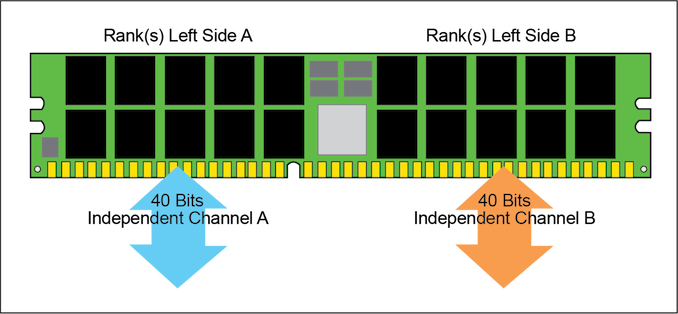
The big change here is that, similar to what we’ve seen in other standards like LPDDR4 and GDDR6, a single DIMM is being broken down into 2 channels. Rather than one 64-bit data channel per DIMM, DDR5 will offer two independent 32-bit data channels per DIMM (or 40-bit when factoring in ECC). Meanwhile the burst length for each channel is being doubled from 8 bytes (BL8) to 16 bytes (BL16), meaning that each channel will deliver 64 bytes per operation. Compared to a DDR4 DIMM, then, a DDR5 DIMM running at twice the rated memory speed (identical core speeds) will deliver two 64-byte operations in the time it takes a DDR4 DIMM to deliver one, doubling the effective bandwidth.


Overall, 64 bytes remains the magic number for memory operations as this is the size of a standard cache line. A larger burst length on DDR4-style memory would have resulted in 128-byte operations, which is too big for a single cache line, and at best, would have resulted in efficiency/utilization losses should a memory controller not want two lines’ worth of sequential data. By comparison, since DDR5’s two channels are independent, a memory controller can request 64 bytes from separate locations, making it a better fit to how processors actually work and avoiding the utilization penalty.


The net impact for a standard PC desktop then would be that instead of today’s DDR4 paradigm of two DIMMs filling two channels for a 2x64bit setup, a DDR5 system will functionally behave as a 4x32bit setup. Memory will still be installed in pairs – we’re not going back to the days of installing 32-bit SIMMs – but now the minimum configuration is for two of DDR5’s smaller channels.


This structural change also has some knock-on effects elsewhere, particularly to maximize usage in these smaller channels. DDR5 introduces a finer-grained bank refresh feature, which will allow for some banks to refresh while others are in use. This gets the necessary refresh (capacitor recharge) out of the way sooner, keeping latencies in check and making unused banks available sooner. The maximum number of bank groups is also being doubled from 4 to 8, which will help to mitigate the performance penalty from sequential memory access.


Rapid Bus Service: Decision Feedback Equalization


In contrast finding ways to increase the amount of parallelization within a DRAM DIMM, increasing the bus speed is both simpler and harder: the idea is simple in concept and harder in execution. At the end of the day to double DDR’s memory speeds, DDR5’s memory bus needs to run at twice the rate of DDR4’s.


There are several changes to DDR5 to make this happen, but surprisingly, there aren’t any massive, fundamental changes to the memory bus such as QDR or differential signaling. Instead, JEDEC and its members have been able to hit their targets with a slightly modified version of the DDR4 bus, albeit one that has to run at tighter tolerances.


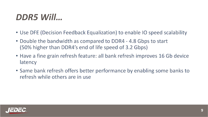
The key driver here is the introduction of decision feedback equalization (DFE). At a very high level, DFE is a means to reduce inter-symbol interference by using feedback from the memory bus receiver to provide better equalization. And better equalization, in turn, allows for the cleaner signaling needed for DDR5’s memory bus to run at higher transfer rates without everything going off the rails. Meanwhile this is further helped by several smaller changes in the standard, such as the addition of new and improved training modes to help DIMMs and controllers compensate for minute timing differences along the memory bus.


Simpler Motherboards, More Complex DIMMs: On-DIMM Voltage Regulation


Along with the core changes to density and memory speeds, DDR5 also once again improves on DDR memory’s operating voltages. At-spec DDR5 will operate with a Vdd of 1.1v, down from 1.2v for DDR4. Like past updates this should improve the memory’s power efficiency relative to DDR4, although the power gains thus far aren’t being promoted as heavily as they were for DDR4 and earlier standards.


JEDEC is also using the introduction of the DDR5 memory standard to make a fairly important change to how voltage regulation works for DIMMs. In short, voltage regulation is being moved from the motherboard to the individual DIMM, leaving DIMMs responsible for their own voltage regulation needs. This means that DIMMs will now include an integrated voltage regulator, and this goes for everything from UDIMMs to LRDIMMs.


JEDEC is dubbing this “pay as you go” voltage regulation, and is aiming to improve/simplify a few different aspects of DDR5 with it. The most significant change is that by moving voltage regulation on to the DIMMs themselves, voltage regulation is no longer the responsibility of the motherboard. Motherboards in turn will no longer need to be built for the worst-case scenario – such as driving 16 massive LRDIMMs – simplifying motherboard design and reining in costs to a degree. Of course, the flip side of this argument is that it moves those costs over to the DIMM itself, but then system builders are at least only having to buy as much voltage regulation hardware as they have DIMMs, and hence the PAYGO philosophy.


According to JEDEC, the on-DIMM regulators will also allow for better voltage tolerances in general, improving DRAM yields. And while no specific promises are being made, the group is also touting the potential for this change to (further) reduce DDR5’s power consumption relative to DDR4.


As the implementation details for these voltage regulators will be up to the memory manufacturers, JEDEC hasn’t said too much about them. But it sounds like there won’t be a one-size-fits-all solution between clients and servers, so client UDIMMs and server (L)RDIMMs will have separate regulators/PMICs, reflecting their power needs.


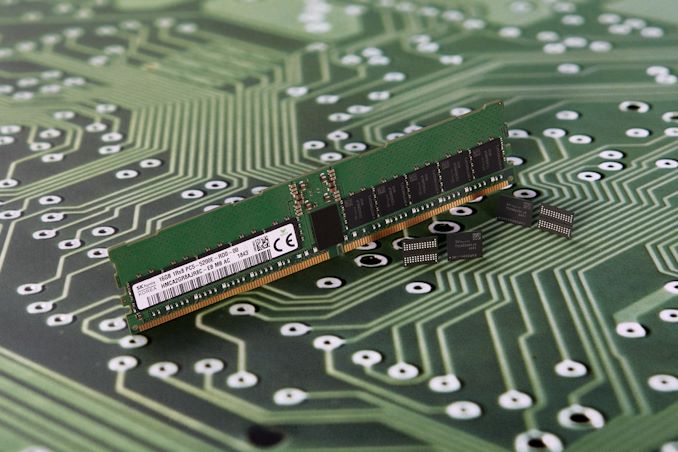
DDR5 DIMMs: Still 288 Pins, But Changed Pinouts


Finally, as already widely demonstrated from earlier vendor prototypes, DDR5 will be keeping the same 288 pin count from DDR4. This mirrors the DDR2 to DDR3 transition, where the pin count was kept identical there as well at 240 pins.


Don’t expect to use DDR5 DIMMs in DDR4 sockets, however. While the pin count isn’t changing the pinout is, in order to accommodate DDR5’s new features – and in particular its dual channel design.


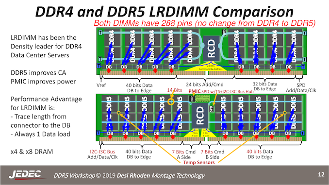
The big change here is that the command and address bus is being shrunk and partitioned, with the pins being reallocated to the data bus for the second memory channel. Instead of a single 24-bit CA bus, DDR5 will have two 7-bit CA busses, one for each channel. 7 is well under half of the old bus, of course, so things are becoming a bit more complex for memory controllers in exchange.


Sampling Now, Adoption Starts in the Next 12-18 Months


Wrapping things up for today’s announcement, like other JEDEC specification releases, today is less of a product launch and more about the development committee setting the standard loose for its members to use. The major memory manufacturers, whom have been participating in the DDR5 development process since the start, have already developed prototype DIMMs and are now looking at wrapping things up to bring their first commercial hardware to market.


The overall adoption curve for DDR5 is expected to be similar to earlier DDR standards. That is to say that JEDEC expects DDR5 to start showing up in devices in 12 to 18 months as hardware is finalized, and increase from there. And while the group doesn’t give specific product guidance, they have been very clear that they expect servers to once again be the driving force behind early adoption, especially with the major hyperscalers. Neither Intel nor AMD have officially announced platforms that will use the new memory, but at this point that’s only a matter of time.


Meanwhile, expect DDR5 to have as long of a lifecycle as DDR4, if not a bit longer. Both DDR3 and DDR4 have enjoyed roughly seven-year lifecycles, and DDR5 should enjoy the same degree of stability. And while seeing out several years with perfect clarity isn’t possible, at this point the JEDEC is thinking that if anything DDR5 will end up with a longer shelf-life than DDR4, thanks to the ongoing maturation of the technology industry. Of course, this is the same year that Apple has dropped Intel for its CPUs, so by 2028 anything is possible.


At any rate, expect to see the major memory manufacturers continue to show off their prototype and commercial DIMMs as DDR5 gets ready to launch. With adoption set to kick off in earnest in 2021, it sounds like next year should bring some interesting changes to the sever market, and eventually the client desktop market as well.


Source: AnandTech – DDR5 Memory Specification Released: Setting the Stage for DDR5-6400 And Beyond

AMD Announces Ryzen Threadripper Pro: Workstation Parts for OEMs Only

Last year we spotted that AMD was in the market to hire a new lead product manager for a ‘workstation division’. This was a categorically different position to the lead PM for high-end desktop, and so we speculated what this actually means. Today, AMD is announcing its first set of workstation products, under the Ryzen Threadripper Pro branding. However, it should be noted that these processors will only be available as part of pre-built systems, and no corresponding consumer motherboards will be made available.


Source: AnandTech – AMD Announces Ryzen Threadripper Pro: Workstation Parts for OEMs Only

PNY Unveils XLR8 Gaming Epic-X RGB DDR4-3200 Memory

Perhaps more widely known for its array of NVIDIA based graphics cards, American based company PNY has announced its latest product, the XLR8 Gaming Epic-X RGB DDR4 memory. Built upon the same lineage as its XLR8 graphics cards, the Epic-X RGB will be available in three capacities ranging from 8 GB to 32 GB kits, with speeds of DDR4-3200.


The PNY XLR8 Gaming Epic-X has been designed around support for X.M.P 2.0 compatible profiles, with speeds of DDR4-3200 and CAS latencies of CL 16. It has an operating voltage of 1.35 V and is available in four different kits. This includes a separately available single 8 GB and 16 GB modules, or in kits of 16 GB (2 x 8 GB) and 32 GB (2 x 16 GB). 


Focusing on the design, the XLR8 Epic-X RGB includes a V-shaped LED bar along the top of the primarily black heatsink, which includes a red and white XLR8 logo in the middle. The RGB LEDs themselves are certified to work with motherboard vendors RGB software for user-friendly control and customization. This includes ASRock’s Polychrome RGB, MSI’s Mystic Light, GIGABYTE’s RGB Fusion, and the ASUS Aura RGB ecosystems. PNY mentions each kit is using preselected memory chips, but it doesn’t specify the type it is using. 


The PNY XLR8 Epic-X RGB memory will be available to buy from the 20th July at Amazon and Best Buy, while customers can also purchase them directly from the PNY online store. The 8 GB single-channel module has an MSRP of $40, the single 16 GB module for $70, while the 16 GB (2 x 8 GB) kit costs $80 and the biggest kit, the 32 GB (2 x 16 GB) will be available for $135.


Related Reading


Source: AnandTech – PNY Unveils XLR8 Gaming Epic-X RGB DDR4-3200 Memory

Google’s new Confidential Virtual Machines on 2nd Gen AMD EPYC

With AMD’s market share slowly increasing, it becomes very interesting to see where EPYC is being deployed. The latest announcement today comes from AMD and Google, with news that Google’s Compute Engine will start to offer new Confidential Virtual Machines (cVMs) built upon AMD’s Secure Encryption Virtualization (SEV) feature. These new cVMs are variants of Google’s N2D series offerings, and Google states that enabling SEV for full memory and virtualization encryption has a near zero performance penalty.


Secure Encryption Virtualization in AMD’s 2nd Gen EPYC processors allows cloud providers to encrypt all the data and memory of a virtual machine at the per-VM level. These are generated on-the-fly in hardware, and are non-exportable, reducing the risk of side attacks by potentially aggressive neighbors. Previously this sort of computing model was only possible if a host assumed control of a whole server, which for most use cases isn’t practical.


With SEV2, technically AMD allows for up to 509 keys per system. Google will offer images for its cVMs with Ubuntu 18.04/20.04, COS v81, and RHEL 8.2; other operating system images will be available in due course.


These cVMs will be available in vCPU listings, confirming that simultaneous multi-threading is enabled on the hardware. Both Google and AMD declined to comment on the exact EPYC CPUs being used, only that they were part of the 2nd Gen Rome family.


This is technically a beta launch, with Google being the first cloud provider to offer SEV-enabled VMs. Google is also promoting the use of its Asylo open-source framework for confidential computing, promising to make deployment easy at a high performance.


A number of 30 MB gifs were created by Google to showcase the new cVMs. Rather than share them with you in an outdated 1989 format, we converted them to video:


Users wanting access to the new VMs should go to the relevant Google page.


Related Reading


Source: AnandTech – Google’s new Confidential Virtual Machines on 2nd Gen AMD EPYC

Analog Devices To Buy Maxim Integrated

Today Analog Devices has announced that it will be acquiring Maxim Integrated in a transaction estimated at $21bn. The combined company value is said to end up being valued at $68bn, creating a significant player in the analog IC market.


Analog Devices are most popularly known by their signal processing discrete ICs, such as amplifiers, ADCs and DACs, although their product portfolio extends to a very wide range of other designs.


Maxim Integrated is most popularly known by their power management ICs as well as sensors. For example, they have been the main the main battery PMIC (And until recent years, a lot of other phone-centric PMICs) provider for Samsung mobile devices for the better part of the last decade.


Although the two companies have some overlapping product segments which likely will see consolidation, the overall two business seem like they will be complementary to each other as they both specialize in different areas. Analog Devices in particular says that the transaction is meant to boost its market share in the automotive and data centre markets thanks to Maxim’s application specific products, while continuing to offer Analog Devices own broader market products.


In a market where we see a ton of consolidation and many vendors opting to vertically integrated their solutions, it becomes important to have a broader product portfolio in order to maintain leadership positions. The new consolidated Analog Devices and Maxim Integrated entity will have the breath to compete against big players such as Texas Instruments.


Source: AnandTech – Analog Devices To Buy Maxim Integrated

Best Intel Motherboards: July 2020

There’s no disputing that Intel had a quiet first half of the year, with not much cadence in its product releases, aside from Comet Lake and its associated Z490 motherboards. During the middle part second quarter, Intel finally unveiled its revamped 14 nm processors through its release of the 10th generation Comet Lake for desktop, and along with it a heap of new models ranging from Z490 to H460, and even the more workstation focused W480 models. Moving firmly into the third quarter of 2020, Intel now has a fully stacked lineup and we’re unveiling our Best Intel Motherboards guide for July 2020.


Source: AnandTech – Best Intel Motherboards: July 2020

Colorful Announces Two sub-$130 micro-ATX B550 Motherboards

With AMD’s B550 models now on the shelves, a lot of focus around its launch was based on pricing – or rather the lack of very low-cost entry-level models.


The motherboard manufacturer Colorful has today unveiled two new micro-ATX sized B550 motherboards: the  CVN B550M Gaming Frozen V14 and B550M Gaming Pro V14 models. Some of the primary features include a Realtek ALC892 HD audio codec, two PCIe M.2 slots with one Gen4 and one Gen3 slot, as well as a Realtek Gigabit Ethernet controller.


The Colorful CVN B550M Gaming Frozen V14 micro-ATX motherboard


The most striking of the new pair from Colorful is the CVN B550M Gaming Frozen V14 model. It features a very aesthetically pleasing white and silver color scheme, with Naval inspired CVN aircraft carrier class branding and an actively cooled chipset heatsink with a red ring around the fan for contrast.


Although the Colorful CVN B550M Gaming Pro 14V follows a black and silver aesthetic, both models share the same feature set, with a full-length PCIe 4.0 x16 slot, a full-length PCIe 3.0 x4 slot, and a small PCIe 3.0 x1 slot. For storage, both models include a single PCIe 4.0 x4 M.2 slot, and a secondary PCIe 3.0 x4 M.2 slot, with four SATA ports that includes support for RAID 0, 1, and 10 arrays. Each model also includes four memory slots with support for up to DDR4-4000, with a maximum capacity of up to 128 GB. Colorful is also advertising a 10-phase power delivery on both boards but doesn’t go into detail in regards to the componentry or design.


The Colorful CVN B550M Gaming Pro V14 micro-ATX motherboard


Neither model includes any USB 3.2 G2 connectivity, but there are three USB 3.2 G1 Type-A, one USB 3.2 G1 Type-C, and two USB 2.0 ports. Also present is a pair of video outputs including HDMI and DisplayPort, with six 3.5 mm audio jacks powered by a Realtek ALC892 HD audio codec. For networking is a single Ethernet port which is powered by a Realtek 8111H Gigabit controller, with a PS/2 combo port which finishes off the pairings rear panels.


The cool-looking Colorful CVN B550M Gaming Frozen V14 has an MSRP of $126, while the black and grey B550M Gaming Pro V14 comes with a slightly cheaper MSRP of $121. Although Colorful hasn’t divulged when or where these models will be available, they are likely to hit stockists of Colorful motherboards in the coming month.


Related Reading


Source: AnandTech – Colorful Announces Two sub-0 micro-ATX B550 Motherboards

Western Digital's 16TB and 18TB Gold Drives: EAMR HDDs Enter the Retail Channel

Western Digital made a number of announcements yesterday related to their enterprise hard-disk drives (HDD) product lines. While there was nothing unexpected in terms of the products being announced, two aspects stood out – one was the retail availability of EAMR (energy-assisted magnetic recording) HDDs, and the other was additional information on the EAMR technology itself. In 2019, WD had announced the sampling of EAMR-based Ultrastar DC datacenter HDDs with 18TB and 20TB capacities. Yesterday’s announcements build upon those products – the WD Gold-branded version of the Ultrastar DC CMR drives is now available for retail purchase, and the Ultrastar drives themselves have moved to general availability. The Ultrastar JBOD and storage server product lines have also been updated to utilize these new high-capacity drives.


Flash-based storage devices have taken over traditional consumer hard-drive application areas. However, increasing data storage requirements mean that HDDs still continue to be the most cost-effective solution for bulk storage. HDD vendors have been working on increasing hard drive capacities using multiple techniques. Around 10 years back, we had 2TB 3.5″ HDDs with five PMR (perpendicular magnetic recording) platters in an air-filled enclosure. These drives were CMR (conventional magnetic recording) drives. In the last decade, we have seen advancements in three different categories that have enabled a 10-fold increase in the capacity of HDDs while retaining the same physical footprint:


Increasing the number of platters / making the platters thinner has been made possible by using sealed helium-filled enclosures. The reduced turbulence enables platters to be stacked closer to each other. The first-generation helium HDDs had 7 platters, and this has now grown to 9 platters for the new high-capacity drives.


The size of the writing head and the flexibility with which it can be manipulated dictate the minimum width of the recording tracks on the platters. Western Digital is claiming that they are the first to use a triple-stage actuator (TSA) in shipping HDDs.


The Triple-Stage Actuator (Picture courtesy: Western Digital)


The enhanced precision with TSA allows the TPI factor to go up. Incidentally, Seagate also has a novel actuator scheme (dual actuator), though that is aimed at increasing the throughput / IOPS.


One of the key challenges faced in the quest to increase the areal density of platters is the ability of the writing head to reliably alter the magnetic state of the grains in the tracks. Both heat-assisted magnetic recording (HAMR) and microwave-assisted magnetic recording (MAMR) are techniques that address this issue. In 2017, WD seemed set to go all-in on MAMR for their HDD product line, but three years down the road, we are looking at a variant that WD claims is a product of their HAMR and MAMR research – EAMR (energy-assisted magnetic recording).


While details were scant when EAMR was announced , WD is finally opening up on some of the technical aspects.


Energy-Assisted PMR (ePMR) (Pictre courtesy: Western Digital)


WD’s first-generation EAMR technology (christened as ePMR) involves the application of electrical current to the writing head’s main pole (this is in addition to the current sent through the voice coil) during write operations. The additional magnetic field created by this bias current ensures that the bits on the track alter their state in a more deterministic manner. In turn, this allows the bits to be packed closer together and increasing the areal density.


The above techniques can also be used with shingled magnetic recording (SMR) to boost areal density further. SMR has been around in both host-managed and drive-managed versions for a few years now. WD indicated in yesterday’s announcement that qualification shipments of their 20TB Ultrastar DC host-managed SMR drive are in progress.


Western Digital’s Gold Series – Enterprise-Class Hard Disk Drives Family Specifications


The WD Gold 18TB is available for purchase today and will set you back by $593. The 16TB version is priced at $528, but is currently out of stock. As is typical for enterprise drives, the two new models each have a MTBF of 2.5M hours, workload rating of 550TB/yr, and a 5 year warranty.


Source: AnandTech – Western Digital’s 16TB and 18TB Gold Drives: EAMR HDDs Enter the Retail Channel

Qualcomm Announces Snapdragon 865+: Breaking the 3GHz Threshold

Today Qualcomm is announcing an update to its extremely successful Snapdragon 865 SoC: the new Snapdragon 865+. The Snapdragon 865 had already seen tremendous success with over 140 different design wins, powering some of the best Android smartphone devices this year. We’re past the hectic spring release cycle of devices, and much like last year with the S855+, for the summer and autumn release cycle, Qualcomm is providing vendors with the option for a higher-performance binned variant of the chip, the new S865+. As a bit of a arbitrary, but also important characteristic of the new chip is that this is the first ever mobile silicon to finally pass the 3GHz frequency mark.


Source: AnandTech – Qualcomm Announces Snapdragon 865+: Breaking the 3GHz Threshold

Intel Thunderbolt 4 Update: Controllers and Tiger Lake in 2020

Wired connectivity is converging onto two standards: USB4 and Thunderbolt 4. Both of these are set to debut by the end of the year in Intel’s upcoming Tiger Lake platform, and to set the scene Intel is updating us on the scope of its Thunderbolt 4 efforts.


Source: AnandTech – Intel Thunderbolt 4 Update: Controllers and Tiger Lake in 2020

Synaptics To Buy Broadcom’s Wireless IoT Business For $250 Million

Synaptics this afternoon is announcing that the firm is acquiring Broadcom’s wireless IoT business unit. The deal will see Synaptics acquire “certain rights” to Broadcom’s Wi-Fi, Bluetooth and GPS products for the IoT market, as well as in-development products and the business relationships themselves. The total bill for the transaction is set to be $250 million, which Synaptics will be paying entirely in cash.


One of the tech industry’s biggest controller suppliers, in the consumer space Broadcom is generally best known (or at least most visible) for its wireless products. The various iterations of the company have produced a number of controllers and chipsets for Wi-Fi, Bluetooth, and other wireless technologies, which have shown up in everything from PCs and smartphones to game consoles and routers. Late last year the company was reportedly planning to sell off its wireless division wholesale, but in recent months has changed its mind and decided to keep the business after securing a major customer win. Instead, it would seem that the company has opted to slice off a smaller part of its wireless business unit, and in turn is selling that to Synaptics.


For its part, according to the company’s press release Synaptics is getting Broadcom’s “wireless IoT” business, which is distinct from their larger wireless unit. Along with current and future hardware for this market, Synaptics is also getting a 60 member engineering support team, as well as limited exclusivity for three years. All told, this is expected to significantly augment Synaptics’ product portfolio, as it will allow them to increase their vertical integration by developing an even larger portion of their IoT hardware and IP in-house.


Overall, buying out Broadcom’s wireless IoT unit is the latest in a series of acquisitions for Synaptics, who for the last few years has been in the process of diversifying its product portfolio. While the company is best known for its human interface technologies, such as trackpads and fingerprint readers, in recent years the company has been branching out into the IoT space in order to broaden and diversify their core businesses. This has included buying out Conexant Systems as well as Marvell’s multimedia unit in 2017, wand now Broadcom’s wireless IoT business is set to join them.


As things stand, the deal is set to close in the first quarter of 2021. Synaptics will be paying for the business unit entirely in cash, with the majority of that coming from the earlier sale of Synaptics’ Touch and Display Integration business.


Meanwhile, on an amusing note, this marks the second time that Broadcom has sold off its IoT business. The company previously sold off its then-wireless IoT business to Cypress Semiconductor in 2016, a deal that eventually closed for $550 million. So while Broadcom doesn’t seem to have much interest in keeping its IoT businesses, the company seems to have found a niche in growing them to sell off.


Source: AnandTech – Synaptics To Buy Broadcom’s Wireless IoT Business For 0 Million

Charles Chiang, President and CEO of MSI, Passes Away at 56

It is on a sad note that we are learning that MSI’s President and CEO, Charles Chiang, has passed away. Charles took the role of CEO a little over a year ago in January 2019, having headed up the massive success of MSI’s Desktop Platform Business Division and the growth in the companies Gaming branding and laser focus these past few years.


Charles had been part of MSI’s life for over 20 years; I have had the pleasure of meeting with him quite frequently in my trips to Taiwan and Computex, as well as an extensive HQ tour when MSI’s gaming brand was first starting – we discussed the upcoming emergence of virtual reality and how MSI wanted to create the world’s first VR-ready notebook. Charles always had time to listen to my industry ramblings, and was always keen to showcase how he perceived the industry with his decades of insight. He will be missed.


Going for Gaming: An Interview with MSI VP Charles Chiang on Gaming and Strategy


The following statement was given to Tom’s Hardware from MSI:


“Earlier today, MSI GM and CEO Charles Chiang passed away. Having been a part of the company for more than 20 years, he made outstanding contributions and was admired by his colleagues. Mr. Chiang was a respected leader in the MSI family, and helped pave the way for the brand’s success. We are all deeply saddened by the news, and are mourning the loss of Mr. Chiang. He will be deeply missed by the entire team.”


Our condolences go out to his family and to MSI.


Source: AnandTech – Charles Chiang, President and CEO of MSI, Passes Away at 56

Deepcool Releases Castle 280EX AIO CPU Cooler

Further expanding its ever-growing list of CPU coolers, Deepcool has announced its new Castle 280EX AIO CPU cooler, a closed loop liquid cooler with a 280 mm radiator. Slotting in between the pre-existing Castle 240EX and 360EX, the 280EX is designed to improve options for users looking for an RGB-infused cooler with a grey cylindrical CPU block.


The Deepcool Castle EX series is designed with a 3-phase motor intended to improve flow rate and overall cooling performance, but with less operating noise. The latest in the Castle EX range is the 280EX, which uses a 280 mm radiator that’s paired with a black sprayed aluminium core, and comes supplied with a pair of 140 mm 400-1600 rpm cooling fans. The new cooler supports all the usual socket types, including Intel’s LGA20XX, LGA 1200 and LGA 115x sockets, as well as AMD’s TRX40/TR4 and AM4 sockets.


One of the Deepcool Castle 280EX’s main design traits comes via the CPU block and pump, with a swappable logo plate which allows users to choose between Deepcool’s Gamerstorm emblem or a ying-yang symbol. Integrated into the rather bulky looking pump and block is some addressable RGB LED lighting which can be customized through a 3-pin ARGB motherboard header, or with an included RGB controller in the accessories bundle.


The cooling plate is made from copper for effective heat dissipation, and Deepcool has opted for a larger design with 25% more skived fins, although Deepcool doesn’t state which model it is using as a comparison. The larger plate allows better support for the sizable AMD TR4 socket, which has a much larger IHS than smaller processors such as the AMD’s Ryzen 3000 series.


The Deepcool Castle 280EX has an MSRP of $150 and is currently available to buy at Amazon. For reference, the larger Castle 360EX is presently available for $158, while the smallest of the now completed trio, the 240EX with 240 mm radiator can be purchased for $130.


Related Reading


Source: AnandTech – Deepcool Releases Castle 280EX AIO CPU Cooler

Intel Marks Gemini Lake Atom Platform for End-of-Life

Alongside Intel’s Skylake Core CPU architecture, Intel’s other CPU workhorse architecture for the last few years has been the Goldmont Plus Atom core. First introduced in 2017 as part of the Gemini Lake platform, Goldmont Plus was a modest update to Intel’s Atom architecture that has served as the backbone of the cheapest Intel-based computers since 2017. However Goldmont Plus’s days have been numbered since the announcement of the Tremont Atom architecture, and now Goldmont Plus is taking another step out the door with the announcement that Intel has begun End-Of-Life procedures for the Gemini Lake platform.


Intel’s bread and butter budget platform for the last few years, Gemini Lake chips have offered two or four CPU cores, as well as the interesting UHD Graphics 600/605 iGPUs, which ended up incorporating a mix of Intel’s Gen9 and Gen10 GPU architectures. These chips have been sold under the Pentium Silver and Celeron N-series brands for both desktop and mobile use, with TDPs ranging from 6W to 10W. All told, Gemini Lake doesn’t show up in too many notable PCs for obvious reasons, but it has carved out a bit of a niche in mini-PCs, where its native HDMI 2.0 support and VP2 Profile 2 support (for HDR) have given it a leg up over intel’s 7th/8th/9th generation Core parts.


None the less, after almost 3 years in the market Gemini Lake’s days are numbered. In the long-run, it’s set to be replaced with designs using Intel’s new Tremont architecture. Meanwhile in the short-run Intel’s budget lineup will be anchored by the Gemini Lake Refresh platform, which Intel quietly released in late 2019 as a stopgap for Tremont. As a result, Intel has started the process for retiring the original Gemini Lake platform, as the OG platform has become redundant.


Under a set of Product Change Notifications published yesterday, Intel has laid out a pretty typical EOL plan for the processors. Depending on the specific SKU, customers have until either October 23rd or January 22nd to make their final chip orders. Meanwhile those final orders will ship by April 2nd of 2021 or July 9th of 2021 respectively.


All told, this gives customers roughly another year to wrap up business with a platform that itself was supplanted the better part of a year ago.


Sources: Intel, Intel, & Intel


Source: AnandTech – Intel Marks Gemini Lake Atom Platform for End-of-Life

New AMD Ryzen 3000XT Processors Available Today

Announced a couple of weeks ago, the new AMD Ryzen 3000XT models with increased clock frequencies should be available today in primary markets. These new processors offer slightly higher performance than their similarly named 3000X counterparts for the same price, with AMD claiming to be taking advantage of a minor update in process node technology in order to achieve slightly better clock frequencies.


Source: AnandTech – New AMD Ryzen 3000XT Processors Available Today

xMEMS Announces World's First Monolithic MEMS Speaker

Speakers aren’t traditionally part of our coverage, but today’s announcement of xMEMS’ new speaker technology is something that everybody should take note of. Voice coil speakers as we know them and have been around in one form or another for over a hundred years and have been the basis of how we experience audio playback.


In the last few years, semiconductor manufacturing has become more prevalent and accessible, with MEMS (Microelectromechanical systems) technology now having advanced to a point that we can design speakers with characteristics that are fundamentally different from traditional dynamic drivers or balanced armature units. xMEMS’ “Montara” design promises to be precisely such an alternative.


xMEMS is a new start-up, founded in 2017 with headquarters in Santa Clara, CA and with a branch office in Taiwan. To date the company had been in stealth mode, not having publicly released any product till today. The company’s motivations are said to be breaking decades old speaker technology barriers and reinventing sound with new innovative pure silicon solutions, using extensive experience that its founders have collected over years at different MEMS design houses.


The manufacturing of xMEMS’ pure silicon speaker is very different to that of a conventional speaker. As the speaker is essentially just one monolithic piece manufactured via your typical lithography manufacturing process, much like how other silicon chips are designed. Due to this monolithic design aspect, the manufacturing line has significantly less complexity versus voice coil designs which have a plethora of components that need to be precision assembled – a task that is quoted to require thousands of factory workers.


The company didn’t want to disclose the actual process node of the design, but expect something quite crude in the micron range – they only confirmed that it was a 200mm wafer technology.


Besides the simplification of the manufacturing line, another big advantage of the lithographic aspect of a MEMS speaker is the fact that its manufacturing precision and repeatability are significantly superior to that of a more variable voice coil design. The mechanical aspects of the design also has key advantages, for example higher consistency membrane movement which allows higher responsiveness and lower THD for active noise cancellation.


xMEMS’ Montara design comes in an 8.4 x 6.06 mm silicon die (50.9mm²) with 6 so-called speaker “cells” – the individual speaker MEMS elements that are repeated across the chip. The speaker’s frequency response covers the full range from 10Hz to up to 20KHz, something which current dynamic driver or balanced armature drivers have issues with, and why we see multiple such speakers being employed for covering different parts of the frequency range.


The design is said to have extremely good distortion characteristics, able to compete with planar magnetic designs and promises to have only 0.5% THD at 200Hz – 20KHz.


As these speakers are capacitive piezo-driven versus current driven, they are able to cut power consumption to fractions of that of a typical voice coil driver, only using up 42µW of power.


Size is also a key advantage of the new technology. Currently xMEMS is producing a standard package solution with the sound coming perpendicularly out of the package which has the aforementioned 8.4 x 6.05 x 0.985mm footprint, but we’ll also see a side-firing solution which has the same dimensions, however allows manufacturers to better manage internal earphone design and component positioning.


In the above crude 3D printed unit with no optimisations whatsoever in terms of sound design, xMEMS easily managed to design an earphone of similar dimensions to that of current standard designs. In fact, commercial products are likely to looks much better and to better take advantage of the size and volume savings that such a design would allow.


One key aspect of the capacitive piezo-drive is that it requires a different amplifier design to that of classical speaker. Montara can be driven up to 30V peak-to-peak signals which is well above the range of your existing amplifier designs. As such, customers wishing to deploy a MEMS speaker design such as the Montara requires an additional companion chip, such as Texas Instruments’ LM48580.


In my view this is one of the big hurdles for more widespread adoption of the technology as it will limit its usage to more integrated solutions which do actually offer the proper amplifier design to drive the speakers – a lot of existing audio solutions out there will need an extra adapter/amp if any vendor actually decides to actually make a non-integrated “dumb” earphone design (As in, your classical 3.5mm ear/headphones).


TWS (True wireless stereo) headphones here obviously are the prime target market for the Montara as the amplifier aspect can be addressed at design, and such products can fully take advantage of the size, weight and power advantages of the new speaker technology.


In measurements, using the crude 3D-printed earphone prototype depicted earlier, xMEMS showcases that the Montara MEMS speaker has significantly higher SPL than any other earphone solution, with production models fully achieving the targeted 115dB SPL (The prototype only had 5 of the 6 cells active). The native frequency response here is much higher in the higher frequencies – allowing vendors headroom in order adapt and filter the sound signature in their designs. Filtering down is much easier than boosting at these frequencies.


THD at 94dB SPL is also significantly better than even an unnamed pair of $900 professional IEMs – and again, there’s emphasis that this is just a crude design with no audio optimisations whatsoever.


In terms of cost, xMEMS didn’t disclose any precise figure, but shared with us that it’ll be in the range of current balanced armature designs. xMEMS’ Montara speaker is now sampling to vendors, with expected mass production kicking in around spring next year – with commercial devices from vendors also likely to see the light of day around this time.


Source: AnandTech – xMEMS Announces World’s First Monolithic MEMS Speaker

SK Hynix: HBM2E Memory Now in Mass Production

Just shy of a year ago, SK Hynix threw their hat into the ring, as it were, by becoming the second company to announce memory based on the HBM2E standard. Now the company has announced that their improved high-speed, high density memory has gone into mass production, offering transfer rates up to 3.6 Gbps/pin, and capacities of up to 16GB per stack.


As a quick refresher, HBM2E is a small update to the HBM2 standard to improve its performance, serving as a mid-generational kicker of sorts to allow for higher clockspeeds, higher densities (up to 24GB with 12 layers), and the underlying changes that are required to make those happen. Samsung was the first memory vendor to ship HBM2E with their 16GB/stack Flashbolt memory, which runs at up to 3.2 Gbps in-spec (or 4.2 Gbps out-of-spec). This in turn has led to Samsung becoming the principle memory partner for NVIDIA’s recently-launched A100 accelerator, which was launched using Samsung’s Flashbolt memory.


Today’s announcement by SK Hynix means that the rest of the HBM2E ecosystem is taking shape, and that chipmakers will soon have access to a second supplier for the speedy memory. As per SK Hynix’s initial announcement last year, their new HBM2E memory comes in 8-Hi, 16GB stacks, which is twice the capacity of their earlier HBM2 memory. Meanwhile, the memory is able to clock at up to 3.6 Gbps/pin, which is actually faster than the “just” 3.2 Gbps/pin that the official HBM2E spec tops out at. So like Samsung’s Flashbolt memory, it would seem that the 3.6 Gbps data rate is essentially an optional out-of-spec mode for chipmakers who have HBM2E memory controllers that can keep up with the memory.


At those top speeds, this gives a single 1024-pin stack a total of 460GB/sec of memory bandwidth, which rivals (or exceeds) most video cards today. And for more advanced devices which employ multiple stacks (e.g. server GPUs), this means a 6-stack configuration could reach as high as 2.76TB/sec of memory bandwidth, a massive amount by any measure.


Finally, for the moment SK Hynix isn’t announcing any customers, but the company expects the new memory to be used on “next-generation AI (Artificial Intelligence) systems including Deep Learning Accelerator and High-Performance Computing.” An eventual second-source for NVIDIA’s A100 would be among the most immediate use cases for the new memory, though NVIDIA is far from the only vendor to use HBM2. If anything, SK Hynix is typically very close to AMD, who is due to launch some new server GPUs over the next year for use in supercomputers and other HPC systems. So one way or another, the era of HBM2E is quickly ramping up, as more and more high-end processors are set to be introduced using the faster memory.


Source: AnandTech – SK Hynix: HBM2E Memory Now in Mass Production

The Intel Lakefield Deep Dive: Everything To Know About the First x86 Hybrid CPU

For the past eighteen months, Intel has paraded its new ‘Lakefield’ processor design around the press and the public as a paragon of new processor innovation. Inside, Intel pairs one of its fast peak performance cores with four of its lower power efficient cores, and uses novel technology in order to build the processor in the smallest footprint it can. The new Lakefield design is a sign that Intel is looking into new processor paradigms, such as hybrid processors with different types of cores, but also different stacking and packaging technologies to help drive the next wave of computing. With this article, we will tell you all you need to know about Lakefield.


Source: AnandTech – The Intel Lakefield Deep Dive: Everything To Know About the First x86 Hybrid CPU