Intel Previews 4-Layer 3D XPoint Memory For Second-Generation Optane SSDs

As part of Intel’s Architecture Day 2020 presentations, Raja Koduri spent a bit of time talking about the status of their Optane products. Most of it was a recapitulation of details Intel has previously shared. The two important Optane product updates planned for this year are the Barlow Pass second-generation Optane DC Persistent Memory Modules (DCPMM) and the Alder Stream second-generation Optane NVMe SSDs.


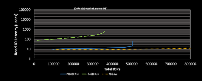
Intel has been teasing their Alder Stream second-generation Optane SSDs since last fall, with promises of off-the-charts performance increases. They’ve confirmed that Alder Stream will be using second-generation 3D XPoint memory, which moves from two to four layers (“decks” in Intel’s slides), making this the first test of the vertical scaling potential of 3D XPoint technology. This combined with with a new SSD controller supporting PCIe 4.0 will enable “multiple millions” of IOPS, more than doubling the throughput of current Optane SSDs. Raja also mentioned that they’ve made optimizations to single-sector reads, so 4kB QD1 random read latency should be improved a bit as well—but this latency is already substantially limited by the latency of PCIe and NVMe command processing.


Intel recently stated that they have not yet decided where to spun up their own volume manufacturing of 3D XPoint memory, so the second-gen 3D XPoint used in Alder Stream will still be manufactured by former partner Micron and purchased by Intel.


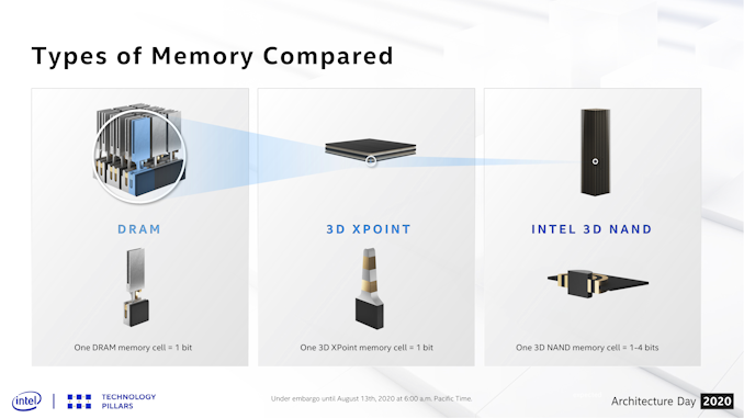
DRAM, 3D XPoint and 3D NAND memories, approximately to scale


Barlow Pass has already launched alongside Cooper Lake Xeons and will be the Optane DCPMM product for Ice Lake Xeons as well. Intel claims an average of 25% higher bandwidth for Barlow Pass than the initial Apache Pass modules for Cascade Lake Xeons.


The fine print in Intel’s slides indicates that the 4-deck 3D XPoint memory used in Alder Stream Optane SSDs is not yet in mass production. That and the omission of any mention of the second-generation, 4-deck 3D XPoint memory in the context of Optane DCPMM products all but confirms that Barlow Pass is still using first-gen 3D XPoint memory. This is consistent with the more modest 25% bandwidth increase as compared to the drastic improvements due to arrive with the Alder Stream SSDs.  It appears that Ice Lake servers will be getting more advanced Optane SSDs than Optane DCPMM modules, as the next generation of Optane DCPMM isn’t due until the launch of Sapphire Rapids processors and the switch to DDR5.


Related Reading


Source: AnandTech – Intel Previews 4-Layer 3D XPoint Memory For Second-Generation Optane SSDs

Intel’s 11th Gen Core Tiger Lake SoC Detailed: SuperFin, Willow Cove and Xe-LP

At the start of the year, Intel ‘foolishly’ handed me a wafer of its next generation Tiger Lake processors, as the moment it came into my hands I attempted to make a very quick exit. In my time with the wafer, we learned that this new 10nm laptop-focused processor had four cores, used Intel’s next generation Xe graphics architecture, and would set the stage at the end of the year as the cornerstone of Intel’s mobile processor offerings. As part of Intel’s Architecture Day 2018 a couple of days ago, the company went into detail about what makes Tiger Lake the true vehicle for 10nm, and why customers will want a Tiger Lake device.


Source: AnandTech – Intel’s 11th Gen Core Tiger Lake SoC Detailed: SuperFin, Willow Cove and Xe-LP

The Intel Xe-LP GPU Architecture Deep Dive: Building Up The Next Generation

As part of today’s Intel Architecture Day, Intel is devoting a good bit of its time to talking about the company’s GPU architecture plans. Though not a shy spot for Intel, per-se, the company is still best known for its CPU cores, and the amount of marketing attention they’ve put into the graphics side of their business has always been a bit weaker as a result. But, like so many other things at Intel, times are changing – not only is Intel devoting ever more die real estate to GPUs, but over the next two years they are transitioning into a true third player in the PC GPU space, launching their first new discrete GPU in several generations.


Source: AnandTech – The Intel Xe-LP GPU Architecture Deep Dive: Building Up The Next Generation

Microsoft Opens Pre-Orders for Surface Duo – US Only

Late last year in October, Microsoft had announced the Surface Duo, the company’s first ever Android device and first-party smartphone (if you can call it that) release in years. What makes the Surface Duo special is its symmetric dual-screen nature and 360° hinge mechanism that allows the device to fold itself shut like a book – to fully opening itself up with two opposing displays. Today Microsoft is finally making the Surface Duo available for pre-order – although availability will be limited to the US.


Microsoft Surface Duo
  Surface Duo
SoC Qualcomm Snapdragon 855 

1x Kryo 485 (Cortex-A76) @ 2.84GHz

3x Kryo 485 (Cortex-A76) @ 2.42GHz

4x Kryo 485 (Cortex-A55) @ 1.80GHz


Adreno 640 @ 585MHz

DRAM 6GB LPDDR4X
Display Dual 5.6″ solid OLED with 360° hinge
1800 x 1350 (4:3)


Unfolded 8.1″ effective diagonal at 2700×1800 (3:2)

Size Height 145.2 mm
Width 93.3 mm (closed) – 186.9 mm (open)
Depth 9.9mm (closed) – 4.8 mm (open)
Weight 250 grams
Battery Capacity 3577mAh total (dual cells)
Wireless Charging
Rear Cameras
Main 11MP 1.0 µm
f/2.0
Telephoto
Wide
Extra
Front Camera
Storage 128 / 256 GB UFS 3.0
I/O USB-C
Wireless (local) 802.11ac Wave 2 Wi-Fi

Bluetooth 5.0 LE + NFC
Cellular (Category 12/5)

DL = 1200Mbps

5x20MHz CA, 256-QAM


UL = 150Mbps

2x20MHz CA, 64-QAM

Other Features It folds
Dual-SIM 1x nanoSIM + eSIM
Launch Price $1399

Starting off with the uninteresting stuff – the internal hardware of the Surface Duo isn’t all that exciting as it features a last generation Snapdragon 855 SoC. Given the device’s early announcement last year it seems Microsoft took a long time to bring the device to market. We’re seeing a standard amount of DRAM and storage space with 6GB and either 128GB or 256GB options. All in all there’s nothing too special about the internals here and are in line with 2019 flagships.


The device’s key characteristic is naturally its symmetrical folding design with two 5.6” 1800 x 1350 resolution OLED screens. Although we call this a folding device, this doesn’t actually apply to the displays as they’re two distinct units covered with solid glass.


Further unique to the design is the hinge mechanism which is symmetrical as well – it allows for a full 360° tilt of the two sides, meaning you can have the device either fully shut, or you can have it fully opened with both screen facing outwards.


Microsoft opted for relatively unusual form-factors here as the screens are each 4:3 – and when opened up it gives you a sort of effective 8.1” diagonal 3:2 surface to work with.


The dimensions of the device come at 145.2mm height in portrait mode, and one side is 93.3mm wide, which opens up till 186.9mm. Each half is extremely thin at only 4.8mm meaning that even when folded it remains a relatively reasonable 9.9mm in thickness.


The device’s 360° folding nature means that the internal screen surface can face completely outwards, and Microsoft took advantage of this for their camera design, of which the Surface Duo only has a single unit. The 11MP 1µm pixel f/2.0 standard wide-angle unit is relatively conservative in specifications, but that’s the compromise that had to be made to fit into a 4.8mm thick chassis and not having the possibility to employ a camera bump.


Microsoft positions the Surface Duo as a productivity device, and its first-party applications such as the Microsoft 365 suite will be optimised for the experience. This seemingly will be the deciding factor as to how the Surface Duo will be received, as it represents quite a niche device market.


The Surface Duo is available for pre-order now at a very high price of $1399, with availability only in the US and compatibility with AT&T, T-Mobile and Verizon, with availability starting September 10th.


The device’s high price and relatively lacklustre specifications will likely result in limited adoption amongst users- and the device in general feels more like an experiment than a product that’s aimed at commercial success.


Related Reading:


Source: AnandTech – Microsoft Opens Pre-Orders for Surface Duo – US Only

Samsung Display Announces First VRR Mobile Display – Inside Note20 Ultra

By now we’ve become quite familiar with high refresh-rate displays in the mobile space, as the first pioneering 90Hz devices last year have now evolved into even faster refreshing 120Hz smartphones becoming the standard. Although all these devices provide augmented user experiences by providing extra smooth scrolling and gaming experiences, they all come with notable compromises when it comes to power efficiency and battery life.


Today, Samsung Display is announcing that they are for the first time revealing new generation display panels that allow for variable refresh rate technology, alleviating one of the biggest draw-backs of current generation high-refresh-rate smartphones. The new technology is makings its debut in the new Galaxy Note20 Ultra, which should be available to the public in just two short weeks.


Currently, the biggest issue for devices using a high refresh rate display is the fact that all current implementation still functions at a certain fixed refresh rate no matter what the screen content is, meaning they always stick to either 60, 90 or 120Hz depending on the smartphone.


This year’s smartphones with 120Hz display in particular have seen the effect of drastically increased power draw when operating under this higher refresh-rate. Although these phones offer the ability to switch between different refresh rates, one cannot call these mechanisms variable refresh rate (VRR) displays as they cannot seamlessly and quickly switch between these modes. As such, even when you’re displaying a fixed static screen, the display continues to refresh at 120Hz and incurs a large power draw penalty, which is less than ideal.


Samsung’s new display panel employed in the new Note20 Ultra is actually described as a VRR panel, with Samsung promising new refresh rate modes such as the ability to operate at 120, 60, 30 and 10Hz modes. The latter super-low refresh rates have been to date never been used in smartphones. Samsung describes that the display will now be able to lower itself down to this new 10Hz mode when viewing static content.


“Existing smartphone panels offer only a fixed refresh rate. They cannot automatically calibrate a phone’s refresh rate, which would result in image flickering caused by luminance differences at lower refresh rates. Samsung Display’s new backplane** technology eliminates flickering for operating frequencies as low as 10Hz.”


Samsung describes the usage of a new backplane technology in order to achieve this – whilst we haven’t had an official response from Samsung to our questions on the matter, there’s been rumours that this is the generation in which the company has introduced LTPO backplane technology, allowing it higher switching performance and lower power consumption.


Another question which remains to be answered is exact details on Samsung’s VRR workings, and whether it is a proper implementation of adaptive sync technology and if it has finer refresh rate granularity in the 10-120Hz beyond just the mentioned 60 and 30Hz examples.


Currently such a VRR implementation would also require a deeper software stack integration into the OS, GPU driver and display driver to fully enable it a seamless operation that would work transparently on any kind of static or low-framerate content – we’ll have to investigate this topic more once Note20 Ultra devices are officially out.


Samsung claims that the new technology should be able to reduce the phone’s display panel power usage by 22% in general use. Furthermore, there’s a statement of it only using 60% of the power of current screens when it is operating in super-low 10Hz mode – although both these figures don’t specify to which baseline they’re being compared to (60 or 120Hz displays?).


Beyond making 120Hz a viable option for daily usage without major battery impact, the new technology should have the potential to improve power efficiency even beyond current 60Hz displays, which hopefully would usher in notably increased battery life in upcoming next-gen devices.


Related Reading:


Source: AnandTech – Samsung Display Announces First VRR Mobile Display – Inside Note20 Ultra

US Appeals Court Reverses Antitrust Ruling in FTC vs Qualcomm

It’s been over three years since the United States FTC had charged Qualcomm with antitrust violations over cellular modem patents and business practices. That suit ultimately received a ruling in May of 2019 against Qualcomm, resulting in an injunction for Qualcomm to renegotiate its licensing agreements with its customers. Qualcomm had subsequently appealed the ruling, putting the order on hold, and today, a bit over a year later, the Ninth Circuit Court of Appeals has finally issued an opinion, reversing and vacating the injunction, resulting in a win for Qualcomm at this moment in time.


The appeals court’s opinion centres around the FTC’s use of anti-trust law to hold Qualcomm accountable for some of its controversial business practices in how it handles licensing of its patent portfolio and its “no license, no chip” mode of operation. The opinion attacks the original judgment in that the arguments presented do not fall under the umbrella of anti-trust law violations, and instead it being a matter of contract and patent law.


The original charge revolved around Qualcomm’s supposed refusal to license cellular patents to competitor chip vendors, with the company countering this accusation that its patents only apply to OEM products, not the chips of components themselves:


“Qualcomm argues that it has no antitrust duty to deal with its rivals, and in any case OEM-level licensing is consistent with Qualcomm’s SSO commitments because only OEM products (i.e., cellphones, tablets, etc.) “practice” or “implement” the standards embodied in Qualcomm’s SEPs. Furthermore, Qualcomm argues that it substantially complies with the TIA and ATIS requirements by not asserting its patents against rival chipmakers.”


The appeals panel has upheld Qualcomm’s notion and point-of-view of the practice, stating that there is no antitrust law which prohibits the company from applying licensing arrangements in this way.


More precisely, the matter of Qualcomm collecting royalties from OEMs is said to be due a change in patent law, that forced the company to stop giving non-exhaustive licenses to other chip vendors:


“… Qualcomm claims that it never granted exhaustive licenses to rival chip suppliers. Instead, as the 1999 email suggests, it entered into “non-exhaustive, royalty-bearing agreements with chipmakers that explicitly did not grant rights to the chipmaker’s customers.” Appellant’s Opening Br. at 45. According to Qualcomm, it ceased this practice in response to developments in patent law’s exhaustion doctrine, see, e.g., Quanta Comput., 553 U.S. at 625 (noting that “the initial authorized sale of a patented item terminates all patent rights to that item”), which made it harder for Qualcomm to argue that it could provide “non-exhaustive” licenses in the form of royalty agreements.”


Because Qualcomm applies this practice equally between all OEMs, and there is no history of the company ever granting exhaustive licenses to a chip vendor, the appeals panel also failed to determine any anticompetitive behaviour on the part of the company, calling Qualcomm’s business model “chip-supplier neutral”, and does not undermine competition in the antitrust market.


“… Qualcomm’s practice of licensing its SEPs exclusively at the OEM level does not amount to anticompetitive conduct in violation of § 2, as Qualcomm is under no antitrust duty to license rival chip suppliers.”


As Qualcomm is seen as not having performed any anticompetitive behaviour in terms of its willingness to license patents to OEMs, and the fact that it gives a “CDMA ASIC” waiver license to chip vendors for free in order for them to internally exercise the technology before they sell it onto their customers, its refusal to give chip vendors non-exhaustive patent licenses is not seen as a matter of antitrust law, and the original ruling to be void in this regard.


The appeal opinion also addresses the third matter of the alleged exclusivity deal that Qualcomm had entered with Apple in 2011 and 2013, that given the effect of this deals had not stifled the competition (And arguing with the fact that Intel had subsequently won Apple contracts in following years), that it also did not go against antitrust law.


Overall, the opinion of the appeals panel today represents a major blow to the FTC and its original legal tactic and usage of antitrust law. Whilst this is a major win for the company, it’s not completely out of the woods as the company’s practises could still be in violation of contract and patent law:


“To the extent Qualcomm has breached any of its FRAND commitments, a conclusion we need not and do not reach, the remedy for such a breach lies in contract and patent law.”


While currently Qualcomm can continue its business practises licensing model, it’s likely to continue to receive future scrutiny in regards to the amount of the fees it charges.


Related Reading:


Source: AnandTech – US Appeals Court Reverses Antitrust Ruling in FTC vs Qualcomm

NUVIA Phoenix Targets +40-50% ST Performance Over Zen 2 for Only 33% the Power

In November 2019, the company NUVIA broke out of stealth mode. Founded by former senior Apple and Google processor architects, John Bruno, Manu Gulati and Gerard Williams III, the company came crashing out of the gate with quite considerable goals to revamp the server market with an SoC that would provide ‘A step-function increase in compute performance and power efficiency’. Today NUVIA is putting more data behind those goals.


Source: AnandTech – NUVIA Phoenix Targets +40-50% ST Performance Over Zen 2 for Only 33% the Power

The NZXT C650 650W PSU Review: Designed To Last

Today we are taking a look at NZXT’s latest PSU, the 650 Watt C-series C650. Aimed at advanced PC users and enthusiasts alike, its basic specs initially seem unimpressive; however digging down reveals a very solid and efficient 80 Plus Gold PSU design underneath. Coupled with 10-year warranty, and the C650 has all the makings of a PSU that’s designed to last.


Source: AnandTech – The NZXT C650 650W PSU Review: Designed To Last

NVIDIA Teases GeForce “Ultimate Countdown” For August 31st: Ampere Inbound?

NVIDIA this morning has posted a short teaser to its GeForce brand Twitter feed, announcing what they are calling the “ultimate countdown”. The pinned Tweet contains a short, abstract video, along with the ultimate countdown hashtag.


Meanwhile and more relevant, the company also updated the banner used in their Twitter profile to reflect their latest marketing campaign, with the additional text of “21 days, 21 years.”


Given the countdown theme of NVIDIA’s new campaign, it’s a reasonable bet that NVIDIA is going to be counting down the next 21 days in preparation for the announcement of something new. Which would have that announcement landing on Monday, August 31st. The 31st, in turn, happens to the 21st anniversary of when the original GeForce 256 (SDR) was announced, which would bring the entire ordeal full-circle.


NVIDIA most recently announced their Ampere GPU architecture and first datacenter product based on it – the A100 accelerator – back in May. That in turn has generated a lot of anticipation for the release of consumer parts based on the new architecture. And with NVIDIA’s current-generation Turing parts about to turn two years old, the company is historically due for a GeForce product refresh.


So we can only assume that NVIDIA is gearing up to announce Ampere gaming parts later this month. Otherwise there are going to be a lot of disappointed gamers come August 31st.


Source: AnandTech – NVIDIA Teases GeForce “Ultimate Countdown” For August 31st: Ampere Inbound?

OPPO's Reno3 5G vs Reno3 Pro vs Reno3 Pro 5G: Why Don't We See More MediaTek Dimensity 1000 Phones?

Today, we’ll be taking a closer look at one of MediaTek’s Dimensity 1000 powered phones, the OPPO Reno3 5G. The Reno3 series has been quite the oddball device line-up this year, as the company has been selectively releasing quite different variants at a rapid pace in different markets – all with different SoCs and slightly differing device specs. We have three of these units at hand, and are going to be taking a closer look at the performance differences of the SoCs.


Source: AnandTech – OPPO’s Reno3 5G vs Reno3 Pro vs Reno3 Pro 5G: Why Don’t We See More MediaTek Dimensity 1000 Phones?

How to Save $6000 on a 28-core Flagship Intel Xeon: Platinum 8280 vs Gold 6258R

In February 2020, Intel launched eighteen new Xeon Scalable second generation processors. These mid-cycle additions to Intel’s product portfolio were designed to bolder up Intel’s server offerings on a very popular and very successful platform, adding in extra cores, extra frequency, or more cache than the previous offerings at roughly the same price. The goal of these ‘performance-oriented’ processors was to address customer requests in offering a more palatable performance-per-dollar offering. One of the new CPUs caught our eye: the Xeon Gold 6258R.


Source: AnandTech – How to Save 00 on a 28-core Flagship Intel Xeon: Platinum 8280 vs Gold 6258R

Intel Suffers Apparent Data Breach, 20GB of IP and Documents Leaked on to Internet

Intel today became the apparent victim of a massive internal data breach, as roughly 20 GB of various Intel documents and tools have begun showing up in a data cache uploaded to the wider internet. With materials seemingly spanning over a decade, the breach reportedly includes everything from Intel presentation templates to BIOS code and debugging tools, and would represent one of the biggest intellectual property leaks from a chipmaker in years.


Released by Till Kottmann, a Swiss software engineer and open security advocate, Kottmann has stated that this is the first of several planned Intel IP releases, calling this first release the “Intel exconfidential Lake Platform Release”. According to tweets posted by Kottmann, he received the material from an anonymous source who breached Intel earlier this year. Meanwhile, ZDNet reports that Kottmann is a regular figure in IP leaks, and has published a number of other tech company leaks before.


Responding to this leak, Intel this afternoon has issued a brief statement to the press acknowledging the leak, and stating that they believe it came form the Intel Resource and Design center, a secure Intel repository for third party partners to access various confidential documents and schematics.


We are investigating this situation. The information appears to come from the Intel Resource and Design Center, which hosts information for use by our customers, partners and other external parties who have registered for access. We believe an individual with access downloaded and shared this data.


While AnandTech has not validated the contents of the data cache, I’ve heard from one source who has seen it that there are signed NDA documents in there mentioning an Intel partner. So while Intel may be right about the source of the data, the actual breach may have occurred with a partner rather than the actual Intel repository, or in concert with a breach of Intel’s repository.


Overall, Kottmann claims that the leak has a wide collection of various Intel confidential and NDA’d documents and tools, including:


  • Intel ME Bringup guides + (flash) tooling + samples for various platforms
  • Kabylake (Purley Platform) BIOS Reference Code and Sample Code + Initialization code (some of it as exported git repos with full history)
  • Intel CEFDK (Consumer Electronics Firmware Development Kit (Bootloader stuff)) SOURCES
  • Silicon / FSP source code packages for various platforms
  • Various Intel Development and Debugging Tools
  • Simics Simulation for Rocket Lake S and potentially other platforms
  • Various roadmaps and other documents
  • Binaries for Camera drivers Intel made for SpaceX
  • Schematics, Docs, Tools + Firmware for the unreleased Tiger Lake platform
  • (very horrible) Kabylake FDK training videos
  • Intel Trace Hub + decoder files for various Intel ME versions
  • Elkhart Lake Silicon Reference and Platform Sample Code
  • Some Verilog stuff for various Xeon Platforms, unsure what it is exactly.
  • Debug BIOS/TXE builds for various Platforms
  • Bootguard SDK (encrypted zip)
  • Intel Snowridge / Snowfish Process Simulator ADK
  • Various schematics
  • Intel Marketing Material Templates (InDesign)

Thus far, while no one has reported finding anything quite as sensitive as Intel CPU or GPU design schematics, the material in the leak looks to be quite valuable, and potentially fairly damaging in the long run. Firmware blobs are particularly interesting, as while these would need to be reverse engineered to extract useful information out of them, they could potentially contain significant information that hasn’t otherwise been shared before.


Otherwise, in a bit of situational irony, this leak is likely to cast doubt upon all future Intel leaks. The inclusion of the company’s presentation templates, while not particularly damaging to Intel, would mean that it’s now trivial to generate fake but accurate-looking Intel roadmaps and presentations. These kinds of materials are already regularly faked, but now it’s easier than ever to do so.


Ultimately with no reason to doubt Kottmann’s claims, it would seem that this just the start of a run of leaks for Intel. And while the company will no doubt be doing everything possible to stop the process, whether they have any legal power to do so remains to be seen.


Source: AnandTech – Intel Suffers Apparent Data Breach, 20GB of IP and Documents Leaked on to Internet

GIGABYTE Updates 4-GPU 2U G242 Server with Rome and PCIe4 for Ampere

As we wait for the big server juggernaut to support PCIe 4.0, a number of OEMs are busy creating AMD EPYC versions to fill that demand for high-speed connectivity. To date there have been two main drivers for PCIe 4.0: high-bandwidth flash storage servers, and high performance CPU-to-GPU acceleration, as seen with the DGX A100. As the new Ampere GPUs roll out in PCIe form, OEMs are set to update their portfolio with new PCIe 4.0-enabled GPU compute servers, including GIGABYTE, with the new G242-Z11.


One of the key elements to a GPU server is enabling airflow through the chassis to provide sufficient cooling for as many 300W accelerators as can fit, not to mention the CPU side of the equation and any additional networking that is required. GIGABYTE has had some good success with its multi-GPU server offerings, and so naturally updating its PCIe 3.0 platform to Rome with PCIe 4.0 was the next step.


The G242-Z11 is a 2U rackmount server that supports four PCIe 4.0 cards with a full x16 link to each. That includes the new A100 Ampere GPUs, as well as AMD MI50 GPUs and networking cards. The system supports any AMD Rome EPYC processor, even the 280W 7H12 built for high-performance tasks, and also has support for up to 2 TB of DDR4-3200 across eight channels with the MZ12-HD3 motherboard.


With these sorts of builds, it is often the periphery that helps assist integration into current infrastructure, and on top of the four PCIe 4.0 accelerators, the G242-Z11 supports two low profile half-length cards and one OCP 3.0 mezzanine card for other features, such as networking. The G242-Z11 also has support for four 3.5-inch SATA pays at the front, and two NVMe/SATA SSD bays in the rear. Power comes from dual 1600W 80 PLUS Platinum power supplies. Remote management is controlled through the AMI MegaRAC SP-X solution, which includes GIGABYTE proprietary server remote management software platform.


The new G242-Z11 will be available from September. Interested parties should contact their local GIGABYTE rep for pricing information.


Source: GIGABYTE


Related Reading


Source: AnandTech – GIGABYTE Updates 4-GPU 2U G242 Server with Rome and PCIe4 for Ampere

MediaTek Announces T700 5G Modem Powering Intel PCs Successfully Certified

Last year, Intel and MediaTek had announced a partnership with the goal of developing a 5G modem that would be used in future next-generation PC platforms. The move followed Intel’s sale of their own cellular modem divison to Apple for $1B.


Today, MediaTek and Intel are announcing the name of the modem, the MediaTek T700 modem, and that the product has passed important milestones in development, having finished the hardware design phase and having been sucessfully certified and tested in real-world 5G SA (Standalone) network calls.


It’s also been announced that Intel is advancing with platform system integration on their part, and readying co-engineering resources and support for OEM partners in order to develop end-products with the Intel and MediaTek platforms.


“Our partnership with Intel is a natural extension of our growing 5G mobile business, and is an incredible market opportunity for MediaTek to move into the PC market,” said MediaTek President Joe Chen. “With Intel’s deep expertise in the PC space and our groundbreaking 5G modem technology, we will redefine the laptop experience and bring consumers the best 5G experiences.”


“A successful partnership is measured by execution, and we’re excited to see the rapid progress we are making with MediaTek on our 5G modem solution with customer sampling starting later this quarter. Building on our 4G/LTE leadership in PCs, 5G is poised to further transform the way we connect, compute and communicate. Intel is committed to enhancing those capabilities on the world’s best PCs,” said Chris Walker, Intel corporate vice president and general manager of Mobile Client Platforms.


The MediaTek’s T700 modem supports sub-6GHz NSA and SA networks, with future generations planned with mmWave connectivity. 


The two companies re-iterate their goal of shipping the first laptops with the 5G modem solutions in early 2021. 


Related Reading:


Source: AnandTech – MediaTek Announces T700 5G Modem Powering Intel PCs Successfully Certified

Intel Schedules Tiger Lake Architecture Presentation For August 13th, Launch on September 2nd

Over the next month or so Intel is scheduled to launch its next-generation Tiger Lake family of processors. Detailed in bits and pieces over the past several months, Tiger Lake will be Intel’s third 10nm-based CPU family and will incorporate the company’s Willow Cove CPU architecture as well as the first integrated GPU based on their new Xe GPU architecture. With that launch quickly approaching, Intel’s investor site has posted notice that the company will be holding two Tiger Lake-related events over the next month, with presentations scheduled for August 13th and September 2nd.


First off, on August 13th Intel will be holding a presentation they’re dubbing “Updates From Our Chief Architect”. The event is set to be run by Raja Koduri, Intel’s chief architect, as well as the general manager of Architecture, Graphics, and Software groups. No other details are being offered about the event at this time – which is typical for investor event announcements – however given Koduri’s background in graphics we can easily make some educated guesses about what will be presented.


Intel to date has offered very little in details about the Xe-LP GPU architecture that will be going into Tiger Lake (and the DG1). So with Koduri helming the event we’re expecting to finally get some major Xe-related graphics architecture disclosures. Whether we should expect to see similar updates for the CPU side of Tiger Lake (Willow Cove) is a bit more nebulous, however; Koduri is Intel’s chief architect for a reason, but it’s well-known that his primary duties at Intel are GPU-related. But regardless of whatever is disclosed, it’s clear that this is going to be an architecture-focused event, as Intel has scheduled a second, later event as the official Tiger Lake launch.


On September 2nd, Intel will be holding their “Tiger Lake Virtual Launch Event”. Even fewer official details are available about this event, but in this case the name says it all. Normally Intel would be holding an in-person event of some kind for the launch of a new CPU platform, however with a coronavirus pandemic going on, everything in the near future is being done virtually. So we’re expecting this event to offer a similar level of detail as past launch events, covering whatever details don’t get included in Intel’s architectural presentation, as well as more direct product details such as SKUs and chip configurations.


Overall, Intel has indicated that they’re planning for a fairly aggressive ramp-up on Tiger Lake – to the tune of 40% more chips than they previously intended – so we should see Tiger Lake products soon after that. However, it’s been a long while since retail products were available day one for an Intel mobile-first launch, so we’re not expecting to have hardware in-hand or in stores on the 2nd.


As always, AnandTech will be covering these events. So please be sure to check in on August 13th and September 2nd for the full scoop on Intel’s Tiger Lake processors and related technologies.


Sources: Intel & Intel


Source: AnandTech – Intel Schedules Tiger Lake Architecture Presentation For August 13th, Launch on September 2nd

Samsung Announces Galaxy Tab S7 & S7+: S865+ & 120Hz Tablets

Today alongside the Note20 series smartphones, Samsung is also releasing a pair of new high-end tablets in the form of the new Tab S7 and Tab S7+. It’s been a long time since we’ve seen some good Android tablets as the market is seemingly small and struggling versus the more common-place Appls iPads – but today’s S7 series is really raising the bar in terms of hardware capabilities, bringing some significant updates to the table for what probably are the best Android tablets on the market right now.


What makes the new Galaxy Tab S7 tablets shine is their brand-new Snapdragon 865+ processors alongside high-resolution 120Hz screens, big batteries, quad-speaker setups and a new design that it’s incredibly thin.


Source: AnandTech – Samsung Announces Galaxy Tab S7 & S7+: S865+ & 120Hz Tablets

Samsung Announces Galaxy Z Fold 2: Second-Generation Foldable

Alongside the new Note20 series smartphones, Samsung is today pre-announcing the brand-new Galaxy Z Fold 2, the successor to last year’s quite controversial Galaxy Fold smartphone, a device which had been marred by manufacturing defects and delays. Today’s coverage of the Z Fold 2 isn’t an actual launch, but rather a pre-announcement ahead of the device’s proper debut in September. Today’s coverage mainly divulges the new phone’s design, with Samsung talking about how they have improved the folding mechanism of the phone and solve some of last year’s issues.


Source: AnandTech – Samsung Announces Galaxy Z Fold 2: Second-Generation Foldable

AZZA Announces Pyramid Mini 806, Unique Pyramid Design Goes Mini-ITX

Back at Computex, we stumbled across a uniquely-styled polyhedron-shaped chassis by AZZA, the Pyramid 804. To cater to small form factor aficionados, AZZA has announced its intention to release a mini-ITX version of its Pyramid 804, the smaller Pyramid Mini 806.


We’ve seen a lot of striking and unique case designs over the last couple of years, some conceptual at trade shows and some beyond that point and in the retail channels. During 2019, AZZA brought to life its Pyramid 804 chassis which is a very notable shape known throughout history. The Pyramids of Giza looks to be the primary inspiration behind the design and is one of the most iconic achievements of humankind.


The AZZA Pyramid Mini 806 mini-ITX chassis builds upon the stylings of the larger sized 806, and is aimed at small form factor enthusiasts looking for a flashy flat for a mini-ITX system. Designed on the premise that the motherboard is mounted horizontally within the case, the frame of the Pyramid Mini 806 is constructed from 1.5 mm thick SPCC rolled steel with 2.0 mm thick aluminum.


It includes support for CPU coolers with a maximum height of up to 85 mm, while video cards with a maximum length of 280 mm can be accommodated the pyramid-shaped chassis. There are two internal 2.5 mm drive bays, with two expansion slots for mini-ITX motherboards which conventionally include a full-length PCIe x16 slot. On the four different sides of the Pyramid Mini 806 are four tempered glass panels, with a single Hurricane II Digital RGB 120 mm cooling fan included in the top. It has limited water cooling support with official support for up to 120 mm radiators, which would suit a 120 mm AIO CPU closed-loop cooler. 


In an isolated chamber located at the bottom of the chassis, there’s space specifically designated for an SFX power supply. Included in the accessories bundle is a 200 mm long PCIe extension cable designed for mounting and connecting a graphics card. There is also a single USB 3.0 header, a front panel audio connector and a power button. The official dimensions of the case are 435 x 368 x 368 mm, with a total weight of 6.3 KG.


Although there is no official date of release, AZZA states that the Pyramid Mini 806 won’t be available until November. AZZA also hasn’t released any pricing information. Still, it is likely to be in the $250-350 price point given its unique design, use of aluminum in its construction, and the additional price premium small form factor chassis generally come with.


Related Reading


Source: AnandTech – AZZA Announces Pyramid Mini 806, Unique Pyramid Design Goes Mini-ITX

Samsung Announces Note 20 & Note 20 Ultra: Better S-Pen, New Finishes

Today Samsung is announcing the much-awaited new Galaxy Note20 and Galaxy Note20 Ultra via its Unpacked August 2020 live stream event. Much like in 2019, Samsung is continuing to offer two variants of the Note series flagship devices, only that this time around the bigger and more feature-rich variants adopts the “Ultra” denomination, with no “+” variant this year. Unlike the Note10 series, this also means that the new Note20 series are also more significantly differing in their specifications, as Samsung is adopting the same differing camera system approaches as on the S20 series, with the Note20 Ultra offering a higher-end camera system compared to the regular Note20.

Naturally, the area where the Note series differentiates itself the most from the S-series is the fact that the phones come with the S-Pen stylus that allows you to write and control the phone with.


Source: AnandTech – Samsung Announces Note 20 & Note 20 Ultra: Better S-Pen, New Finishes