Spotted At Hot Chips: Quad Tile Intel Xe-HP GPU

At last week’s Intel Architecture Day, Intel’s chief architect, Raja Koduri, briefly held up the smallest member of the company’s forthcoming Xe-HP series of server CPUs, the one tile configuration. Now, only a few days later, he has upped the ante by showing off the largest, four tile configuration.


Designed to be a scalable chip architecture, Xe-HP is set to be available with one, two, or four tiles. And while Intel has yet to disclose too much in the way of details on the architecture, based on their packaging disclosures it looks like the company is using their EMIB tech to wire up the GPU tiles, as well as the GPU’s on-package HBM memory.


Assuming it makes it to market, a multi-tiled GPU – essentially multiple GPUs in a single package – would be a major accomplishment for Intel. GPUs are notoriously bandwidth-hungry due to the need to shovel data around between cores, caches, and command frontends, which makes them non-trivial to split up in a chiplet/tiled fashion. Even if Intel can only use this kind of multi-tile scalability for compute workloads, that would have a significant impact on what kind of performance a single GPU package can attain, and how future servers might be built.


Source: AnandTech – Spotted At Hot Chips: Quad Tile Intel Xe-HP GPU

Hot Chips 2020 Live Blog: Intel's Raja Koduri Keynote (2:00pm PT)

Hot Chips has gone virtual this year! Lots of talks on lots of products, including Tiger Lake, Xe, POWER10, Xbox Series X, TPUv3, and a special Raja Koduri Keynote. Stay tuned at AnandTech for our live blogs as we commentate on each talk.


Intel recently had its own Architecture Day 2020, with Raja Koduri and other Intel specialists disclosing details about process and products. It will be interesting to see if Raja discusses anything akin to roadmaps in this keynote.


Source: AnandTech – Hot Chips 2020 Live Blog: Intel’s Raja Koduri Keynote (2:00pm PT)

Hot Chips 2020: Marvell Details ThunderX3 CPUs – Up to 60 Cores Per Die, 96 Dual-Die in 2021

Today as part of HotChips 2020 we saw Marvell finally reveal some details on the microarchitecture of their new ThunderX3 server CPUs and core microarchitectures. The company had announced the existence of the new server and infrastructure processor back in March, and is now able to share more concrete specifications about how the in-house CPU design team promises to distinguish itself from the quickly growing competition that is the Arm server market.

We had reviewed the ThunderX2 back in 2018 – at the time still a Cavium product before the designs and teams were acquired by Marvell only a few months later that year. Ever since, the Arm server ecosystem has been jump-started by Arm’s Neoverse N1 CPU core and partner designs such as from Amazon (Graviton2) and Ampere (Altra), a quite different set of circumstances and alongside AMD’s successful return in the market, a very different landscape.


Source: AnandTech – Hot Chips 2020: Marvell Details ThunderX3 CPUs – Up to 60 Cores Per Die, 96 Dual-Die in 2021

Hot Chips 2020 Live Blog: AMD Ryzen 4000 APU (Noon PT)

Hot Chips has gone virtual this year! Lots of talks on lots of products, including Tiger Lake, Xe, POWER10, Xbox Series X, TPUv3, and a special Raja Koduri Keynote. Stay tuned at AnandTech for our live blogs as we commentate on each talk.


Next up is AMD’s Ryzen 4000 Renoir talk. 


Source: AnandTech – Hot Chips 2020 Live Blog: AMD Ryzen 4000 APU (Noon PT)

Hot Chips 2020 Live Blog: IBM z15, a 5.2 GHz Mainframe CPU (11:00am PT)

Hot Chips has gone virtual this year! Lots of talks on lots of products, including Tiger Lake, Xe, POWER10, Xbox Series X, TPUv3, and a special Raja Koduri Keynote. Stay tuned at AnandTech for our live blogs as we commentate on each talk.


Source: AnandTech – Hot Chips 2020 Live Blog: IBM z15, a 5.2 GHz Mainframe CPU (11:00am PT)

Hot Chips 2020 Live Blog: IBM's POWER10 Processor on Samsung 7nm (10:00am PT)

Hot Chips has gone virtual this year! Lots of talks on lots of products, including Tiger Lake, Xe, POWER10, Xbox Series X, TPUv3, and a special Raja Koduri Keynote. Stay tuned at AnandTech for our live blogs as we commentate on each talk.


Source: AnandTech – Hot Chips 2020 Live Blog: IBM’s POWER10 Processor on Samsung 7nm (10:00am PT)

Hot Chips 2020 Live Blog: Next Gen Intel Xeon, Ice Lake-SP (9:30am PT)

Hot Chips has gone virtual this year! Lots of talks on lots of products, including Tiger Lake, Xe, POWER10, Xbox Series X, TPUv3, and a special Raja Koduri Keynote. Stay tuned at AnandTech for our live blogs as we commentate on each talk. Each one of the 11 or so talks today will get its own self-contained live blog.


Our first talk of the day is from Intel, about its next-generation Ice Lake Xeon Scalable processor. Come back at 9:30am PT and follow along 🙂


Source: AnandTech – Hot Chips 2020 Live Blog: Next Gen Intel Xeon, Ice Lake-SP (9:30am PT)

Intel Brand Tie-ins: New Avengers Packaging Gives You a New Box To Play With

When buying a new processor, what’s the first thing to look for? Price? Performance? Frames per Second? The Box? Intel’s new brand tie-in with Marvel’s Avengers now seems official, according to the @IntelGraphics twitter handle. With the new special edition processors, users can look forward to a brightly painted box. Yes, that’s pretty much it. Oooh, shiny shiny.


Leaks have suggested that these new boxed processors will carry new versions of Intel’s overclockable Comet Lake processors, such as the Core i9-10900K which will become new Core i9-10900KA models in Intel’s database, however we are waiting on confirmation from Intel. 


If this ends up being a success for Intel, no doubt it will set a precedent for future processor tie-ins. It is unclear if this arrangement involves Intel licensing the Marvel brand, or Marvel is paying Intel for co-branding ahead of Marvel’s new videogame, the Marvel Avengers, set to launch on September 4th for Xbox, Playstation, and PC. There have also been suggestions that these processors may also carry codes to download extras for the game, perhaps skins or such, but again this has not been confirmed, nor is it clear that the game has any special Intel-specific acceleration for better gameplay. Imagine if the game detects the CPU string as ‘10900KA’ and offers different abilites or modes – that would certainly interesting as to the mods that would appear to get around that restriction.


Pricing and availability are currently unknown, although we’re expecting more details come September 4th.


Source: Intel Gaming on Twitter


Source: AnandTech – Intel Brand Tie-ins: New Avengers Packaging Gives You a New Box To Play With

Intel Next-Gen 10-micron Stacking: Going 3D Beyond Foveros

One of the issues facing next-generation 3D stacking of chips is how to increase the density of the die-to-die interface. More connections means better data throughput, reducing latency and increasing bandwidth between two active areas of silicon that might be manufactured at different process nodes. There’s also a consideration for power and thermal hotspots as well. Intel has been developing its own physical interconnect topologies, most of which we’ve covered in detail before, such as the Embedded Multi-Die Interconnect Bridge (EMIB) that allows 2D expansion and Foveros die-to-die 3D staking that enables vertical expansion. As part of Intel’s Architecture Day 2020, we have a glimpse into Intel’s future with hybrid bonding.


There are several holistic metrics to measure how ‘good’ an interconnect can be; the two that are easiest to understand are density of connections (bump density) and energy (how much energy it takes to transfer a bit).


Intel’s Ramune Nagisetty showcasing current packaging technologies at Intel


Intel’s own slides show us that EMIB’s bump density is good for ~400 per square millimeter, with a power of 0.50 petajoules per bit transferred. Foveros takes that a step further, supporting 400-1600 bumps per square millimeter, and an average power of 0.15 petajoules per bit transferred.


The next era of ‘Hybrid Bonding’ that Intel is going towards improves both metrics by around a factor of 3-10. The new test chips that Intel has just got back into the lab, involving stacked SRAM, goes towards the 10000 bumps per square millimeter range, with a power under 0.05 petajoules per bit. According to Intel this allows for smaller and simpler circuits, with lower capacitance and better efficiency. Nothing to be said about yields however!


With these new bonding and stacking technologies, the question always becomes one of thermals, and how Intel might stack two performance-related bits of silicon together. In the discussions as part of Architecture Day, Intel stated that these stacked designs require having all layers designed together, rather than independently, in order to manage the electrical and thermal characteristics. As far as Intel sees it, the most power hungry layer is required to go on the top of the stack for the time being, which obviously means that the power connections have to either rise up through the lower layers, or there has to be some form of cantilevered situation where power connections can happen off the edge of the bonding – Intel calls this technology ODI, to support different sized silicon layers.


With the future of high performance and high efficiency computing coming to a head with new packaging technologies, finding the right way of going forward is ever critical. For a context on timeline, Intel’s Ramune Nagisetty has stated that Foveros was patented back in 2008, but it took nearly a decade for the process to become physically viable at scale and high-enough yielding for a product to come to market.


Related Reading


Source: AnandTech – Intel Next-Gen 10-micron Stacking: Going 3D Beyond Foveros

Intel Alder Lake: Confirmed x86 Hybrid with Golden Cove and Gracemont for 2021

Following leaks is often a game of cat and mouse – what is actually legitimate and what might not be. Traditionally AnandTech shies away from leaks for that very reason, and we prefer to have multiple sources that are saying the same thing, rather than addressing every potential rumor on the blogosphere. Nonetheless, hints towards a new product from Intel, Alder Lake, have been cropping up over the past few months, including getting a small mention in Intel’s Q2 2020 earnings. The leaks have suggested that it would offer a mixed Hybrid x86 environment similar to Intel’s current Lakefield product that uses high-performance cores paired with high-efficiency cores. As part of Intel’s Architecture Day 2020, the company officially announced Alder Lake as a hybrid x86 product on its roadmaps.


In the roadmap and as part of the discussions, Intel’s Raja Koduri confirms that Alder Lake will be a combination of the Golden Cove high performance computing core and the Gracemont high efficiency core, and the goal of this chip is to offer a ‘Performance Hybrid’ option into the portfolio. Raja explained to the audience that the company has learned a lot due to building Lakefield, its current hybrid x86 chip for thin and light notebooks, and while Lakefield was focused on battery life, Alder Lake will focus instead on performance.


Alder Lake will involve Intel’s next generation hardware scheduler, which we are told will be able to leverage all cores for performance and make it seamless to any software package. Intel claims that Alder Lake will be Intel’s best (ever? 2021?) performance-per-watt processor.


If leaks are to be believed, then Alder Lake looks set to offer an 8+8 design, although that has not been confirmed. Intel did not go into detail if Alder Lake will involve any next generation packaging, such as Foveros (which Lakefield does) – but in the Q2 2020 financial disclosures, it was said to be positioned for mobile and desktops. We expect Intel to discuss Golden Cove and Gracemont at some point next year, and then Alder Lake as an extension to those – we have already seen Intel documents regarding new instructions for each of these cores. My prediction is to come back this time next year, where we should have more to talk about.


Related Reading


Source: AnandTech – Intel Alder Lake: Confirmed x86 Hybrid with Golden Cove and Gracemont for 2021

Micron Spills on GDDR6X: PAM4 Signaling For Higher Rates, Coming to NVIDIA’s RTX 3090

It would seem that Micron this morning has accidentally spilled the beans on the future of graphics card memory technologies – and outed one of NVIDIA’s next-generation RTX video cards in the process. In a technical brief that was posted to their website, dubbed “The Demand for Ultra-Bandwidth Solutions”, Micron detailed their portfolio of high-bandwidth memory technologies and the market needs for them. Included in this brief was information on the previously-unannounced GDDR6X memory technology, as well as some information on what seems to be the first card to use it, NVIDIA’s GeForce RTX 3090.

The key innovation for GDDR6X appears to be that Micron is moving from using POD135 coding on the memory bus – a binary (two state) coding format – to four state coding in the form of Pulse-Amplitude Modulation 4 (PAM4). In short, Micron would be doubling the number of signal states in the GDDR6X memory bus, allowing it to transmit twice as much data per clock.


Source: AnandTech – Micron Spills on GDDR6X: PAM4 Signaling For Higher Rates, Coming to NVIDIA’s RTX 3090

MMD and Phillips Launch the 279C9 27" Montior: FreeSync 4K IPS & USB Type-C

This week MMD and Phillips have unveiled its latest display in their ever-growing product range, the Phillips 279C9. A 27-inch monitor aimed squarely at content creators and professionals, the 279C9 is based around a 3840 x 2160 60 Hz IPS display and includes features such as a five-port USB hub (including a USB Type-C port), as well as DisplayHDR 400 certification.


Digging into the monitor’s specifications, as is typical with most content-focused monitors in this range, Phillips’ 279C9 has clearly been tuned for its target market. The 3840×2160, 16:9 aspect ratio panel is a very straightforward choice, with MMD tapping an IPS panel for viewing angles and color stability. As this isn’t a gaming-focused display, the monitor tops out at a 60Hz refresh rate, though there is official support for VESA Adaptive Sync to offer variable refresh support and the monitor carries AMD’s FreeSync branding.


Otherwise the 279C9 has a typical static contrast ratio of 1300:1, with “Mega Infinity DCR” smart contrast technology. Meanwhile the monitor is DisplayHDR 400 certified, meaning it can offer 400 nits maximum brightness in HDR mode, and Phillips lists 400 nits as the average brightness as well. The display is framed by a fairly skinny bezel with a 596.74 x 335.66 mm (H x V) viewing area, and the screen itself is coated with an anti-glare 3H coating. 


Meanwhile there is an interesting array of input and output options, including a USB Type-C input, which along with DP alt mode input allows for fast data transfer and official charging support for devices such as laptops. This is joined by dual HDMI 2.0 inputs, as well as a single DisplayPort 1.4 output. As for downstream connectivity, it also includes four USB 3.2 Type-A ports, and while Phillips doesn’t distinguish between the use of USB 3.2 G2 or G1 connectivity, it is likely the latter. Two of the Type-A ports also feature USB fast charging support. Finally, the monitor includes is a pair of 2 W speakers.


Phillips 279C9 27″ Monitor Specifications
Panel 27″ IPS
Native Resolution 3840 x 2160 (16:9)
Maximum Refresh Rate 60 Hz
Response Time 5 ms (grey to grey)
Contrast 1300:1 (Mega Infinity DCR)
Backlight Type W-LED
Viewing Angles 178°/178° Horizontal/Vertical
Aspect Ratio 16:9
Color Gamut NTSC 90.7%

sRGB 109%
DisplayHDR Tier DisplayHDR 400
Inputs 1 x DisplayPort 1.4

2 x HDMI 2.0

1 x USB Type-C (video/data) – 65 W charging

4 x USB Type-A

1 x 3.55 mm headphone out
Audio Dual 2 W Speakers
MSRP (GBP) £449

In terms of availability, Phillips plans to launch the 27″ 279C9 4K display at the end of August, with an MSRP of £449. At present, Phillips hasn’t announced its US pricing or availability outside of the UK market.


Related Reading


Source: AnandTech – MMD and Phillips Launch the 279C9 27″ Montior: FreeSync 4K IPS & USB Type-C

Samsung Announces "X-Cube" 3D TSV SRAM-Logic Die Stacking Technology

Yesterday, Samsung Electronics had announced a new 3D IC packaging technology called eXtended-Cube, or “X-Cube”, allowing chip-stacking of SRAM dies on top of a base logic die through TSVs.


Current TSV deployments in the industry mostly come in the form of stacking memory dies on top of a memory controller die in high-bandwidth-memory (HBM) modules that are then integrated with more complex packaging technologies, such as silicon interposers, which we see in today’s high-end GPUs and FPGAs, or through other complex packaging such as Intel’s EMIB.


Samsung’s X-Cube is quite different to these existing technologies in that it does away with intermediary interposers or silicon bridges, and directly connects a stacked chip on top of the primary logic die of a design.


Samsung has built a 7nm EUV test chip using this methodology by integrating an SRAM die on top of a logic die. The logic die is designed with TSV pillars which then connect to µ-bumps with only 30µm pitch, allowing the SRAM-die to be directly connected to the main die without intermediary mediums. The company this is the industry’s first design such design with an advanced process node technology.


It’s not the first time that the company has demonstrated TSVs in the base logic die to connect to a stacked die on top of it. Back in 2013, the company had showed custom Exynos chips using Widcon technology, stacking Wide I/O DRAM memory on top of the base logic chip with help of TSVs, offering a higher-performance and lower power solution compared to traditional PoP memory. Unfortunately, this technology never saw the light of day in consumer devices as it likely never was cost-effective enough justify for mass-production.


Stacking more valuable SRAM instead of DRAM on top of the logic chip would likely represent a higher value proposition and return-on-investment to chip designers, as this would allow smaller die footprints for the base logic dies, with larger SRAM cache structures being able to reside on the stacked die. Such a large SRAM die would naturally also allow for significantly more SRAM that would allow for higher performance and lower power usage for a chip.


Samsung’s marketing materials showcase more than a single die of SRAM, which would indicate that X-Cube can be variable in terms of its stack-height. It’s currently unclear if X-Cube will be limited to SRAM dies, or whether it will also extend to future logic-over-logic stacking. 


Samsung is providing silicon proven design methodology and flow for its advanced 7nm and 5nm nodes, and states that X-Cube will be utilised for advanced applications such as mobile, AR/VR, wearable and HPC designs. The company is also planning a presentation on X-Cube at Hot Chips this Sunday where it will revealing more details on the technology.


Related Reading:


Source: AnandTech – Samsung Announces “X-Cube” 3D TSV SRAM-Logic Die Stacking Technology

Intel Xe-HPC GPU Status Update: 4 Process Nodes Make 1 Chip

Continuing today’s GPU news from Intel’s Architecture Day presentation, on top of the Xe-LP architecture briefing and Xe-HPG reveal, the company has also offered a brief roadmap update for their flagship sever-level part, Xe-HPC.


Better known by its codename of Ponte Vecchio, much to do has been made about Xe-HPC. The most complex of the Xe parts planned, it is also the cornerstone of the Intel-powered Aurora supercomputer. Xe-HPC is pulling out all of the stops for performance, and to get there Intel is employing every trick in the book, including their new-generation advanced packaging technologies.


The big revelation here is that we finally have some more concrete insight into what manufacturing processes the various tiles will use. The base tile of the GPU will be on Intel’s new 10nm SuperFin process, and the Rambo Cache will be a generation newer still, using Intel’s future 10nm Enhanced SuperFin process. Meanwhile it’s now confirmed that the Xe Link I/O tile, which will be used as part of Intel’s fabric to link together multiple Xe-HPC GPUs, will be built by an external fab.


That leaves the matter of the compute tile, the most performance-critical of the GPU’s parts. With Intel’s 7nm process delayed by at least six months, the company has previously disclosed that they were going to take a “pragmatic” approach and potentially use third-party fabs. And as of their Architecture Day update, they still seem to be undecided about – or at least unwilling to disclose – just what they plan on doing. Instead, the compute die is labeled as “Intel Next Gen & External”.


It’s an unusual disclosure, to say the least, as we’d otherwise expect the compute die to be made on a single process. But with no further commentary from Intel offered, make of that what you will. Perhaps they’re being straightforward, and they will actually use two very different process nodes for the compute die?


Source: AnandTech – Intel Xe-HPC GPU Status Update: 4 Process Nodes Make 1 Chip

Intel’s Xe-HPG GPU Unveiled: Built for Enthusiast Gamers, Built at a Third-Party Fab

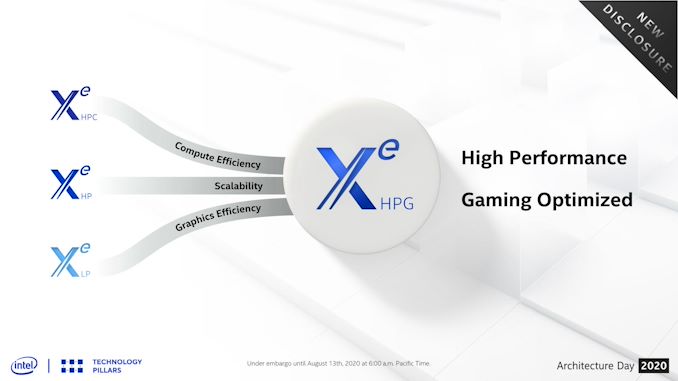
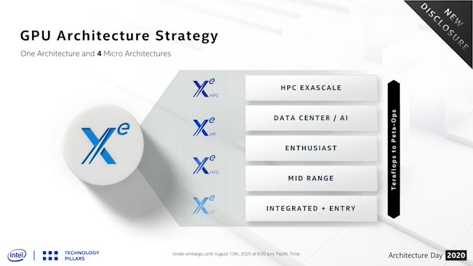
Among the many announcements in today’s Intel Architecture Day, Intel is also offering a major update to their GPU roadmap over the next 24 months. The Xe family, already jam-packed with Xe-LP, Xe-HP, and Xe-HPC parts, is now getting a fourth planned variant: Xe-HPG. Aimed directly at the enthusiast gamer market, this latest Xe variant will be Intel’s most gaming-focused part yet, and the biggest step yet in Intel’s plans to be more diversified in its foundry sources.


So what is Xe-HPG? At a high level, it’s meant to be the missing piece of the puzzle in Intel’s product stack, offering a high-performance gaming and graphics-focused chip. This is as opposed to Xe-HP, which is specializing in datacenter features like FP64 and multi-tile scalability, and Xe-HPC which is even more esoteric. In that respect, Xe-HPG can be thought of as everything in the Xe family, distilled down into a single design to push FLOPs, rays, pixels, and everything else a powerful video card might need.


Like with the rest of Intel’s forward-looking Xe announcements, the company isn’t offering performance projections, features, or the like. But we do have some small details on what to expect.


First and foremost, beyond going after the enthusiast performance space, Intel has confirmed that this part will support ray tracing. A marquee feature of high-end video cards, ray tracing will take on even greater important over the coming years as the soon-to-launch next-generation consoles head out the door with the feature as well, eventually transforming it into a baseline feature across all gaming platforms. Similarly, ray tracing is a critical component of Microsoft’s DirectX 12 Ultimate standard, which given the timing of this GPU and Intel’s intentions, I would be shocked if Intel didn’t support in full.


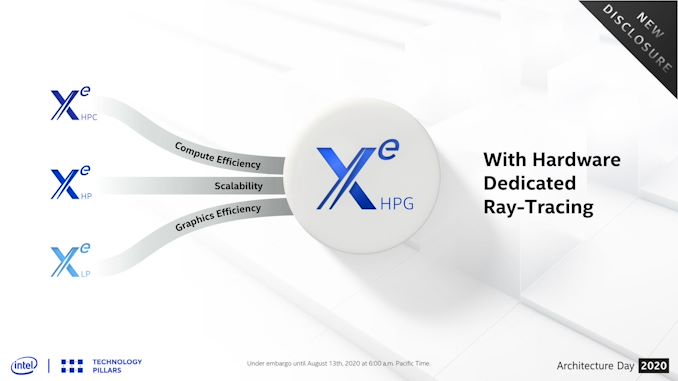
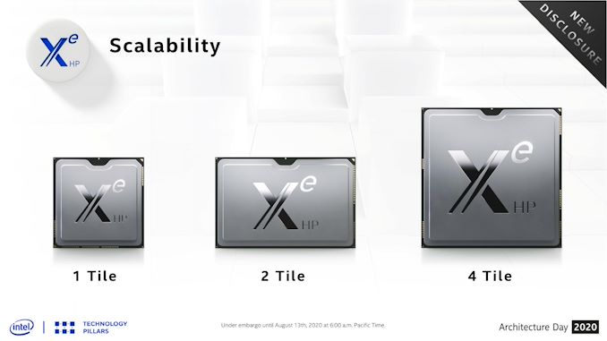
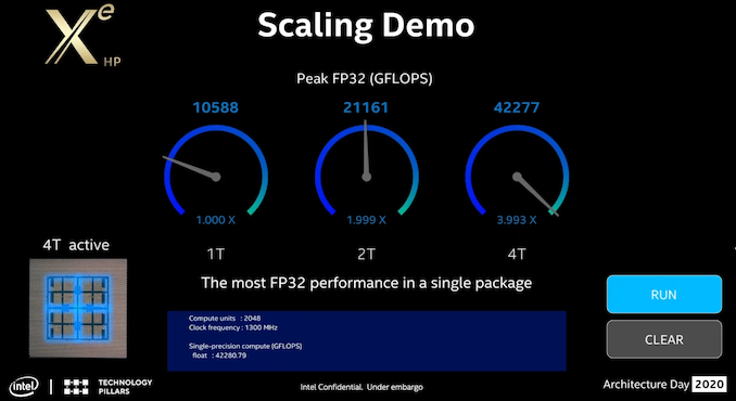
The chip will be built on the foundation that is Xe-LP. However it will also pull in technologies that Intel is pioneering for Xe-HP, and Xe-HPC. Not the least of which is raw scalability, which is being able to take the Xe-LP foundation and scale it up to hundreds (if not thousands) of GPU execution units. But Intel is also pulling what they are calling “compute frequency enhancements” from Xe-HPC, which presumably will allow them to maximize the chip’s overall clockspeeds. All told, I won’t be too surprised if it looks a lot like Xe-HP in general, except with server-driven features like fast FP64 support and multi-tiling stripped out.


But Xe-HPG will also bring something new to the table for the entire Xe family: GDDR6 support. Intel is confirming that the chip – or rather, the microarchitecture the chip will be based on – will be designed to work with GDRR6. This is as opposed to Xe-HP(C), which as high-end server parts use HBM, and Xe-LP, which is designed for use with more conventional memory types. GDDR6 compatibility is a unique need that reflects this is a gaming focused part: GDDR6 provides the memory bandwidth needed for high-performance graphics, but without the stratospheric costs of HBM memory (a problem that has impacted some other high-end GPUs over the years). In a further twist, Intel apparently licensed the GDDR controller IP from outside the company, rather than developing it in-house; so Xe-HPG will have a very notable bit of external IP in it.


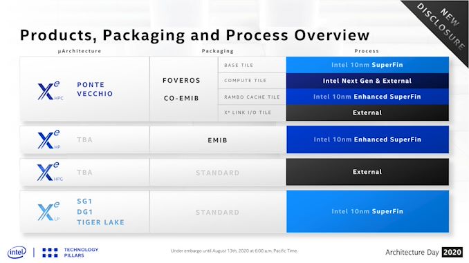
But perhaps most interesting of all for graphics insiders and Intel investors alike is where Xe-HPG will be built: not at Intel. As part of their Architecture Day roadmap, Intel has confirmed that the part will be made at an external fab. In fact it’s the only Xe part where the GPU (or at least the compute element) is being made entirely at a third-party fab. Intel of course will not reveal which fab this is – if it’s TSMC or Samsung – but it means we’re going to see a complete Intel GPU built at another fab. If nothing else, this is going to make comparing Xe-HPG to its AMD and NVIDIA rivals a lot easier, since Intel will be using the same fab resources.


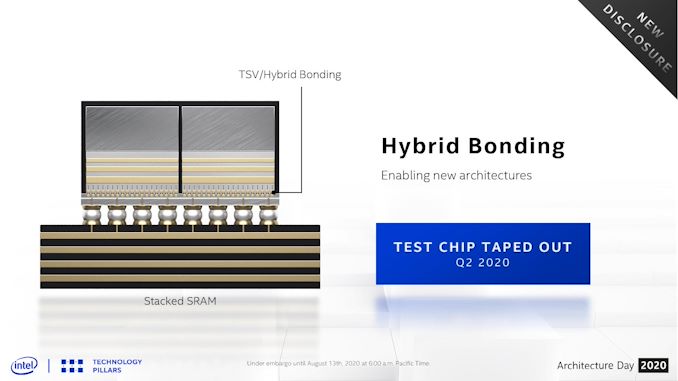
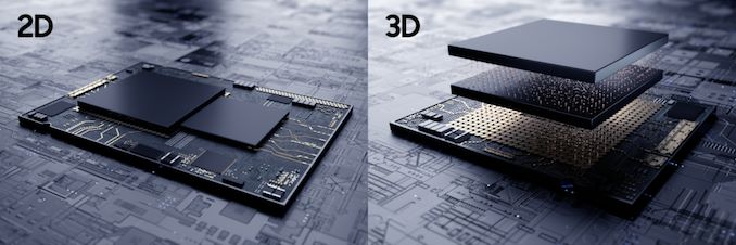
Looking at the same roadmap, it’s worth pointing out that Intel won’t be using any of their advanced packaging technologies for the part. Since they’re not using HBM and they’re not doing multi-tiling, there’s no need for things like EMIB, never mind Foveros. There’s still a lot of unknowns with the cost aspects of Intel’s advanced packaging technologies, so keeping it out of Xe-HPG will presumably help keep costs in check in a very competitive marketplace.


And that is the scoop on Xe-HPG. The latest and most gaming-focused member of Intel’s Xe GPU product stack is set to launch in 2021 – and as Intel looks to break into the wider GPU market, I don’t doubt for a second that this won’t be the last we’ll hear of it between then and now.


Source: AnandTech – Intel’s Xe-HPG GPU Unveiled: Built for Enthusiast Gamers, Built at a Third-Party Fab