Where are my GAA-FETs? TSMC to Stay with FinFET for 3nm

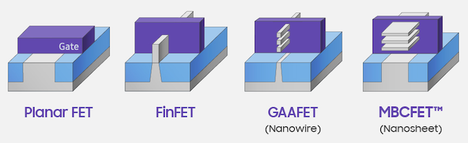
As we passed that 22nm to 16nm barrier, almost all the major semiconductor fabrication companies on the leading edge transitioned from planar resistors to FinFET transistors. The benefits of FinFET were numerous, including better drive currents and lower leakage, better scalability, faster switching times, and an overall better transistor of choice for semiconductor logic. With FinFETs, and multiple rounds of improvements, the technology has scaled from Intel’s first 22nm products down to the 5nm products we will see from TSMC’s partners this year.


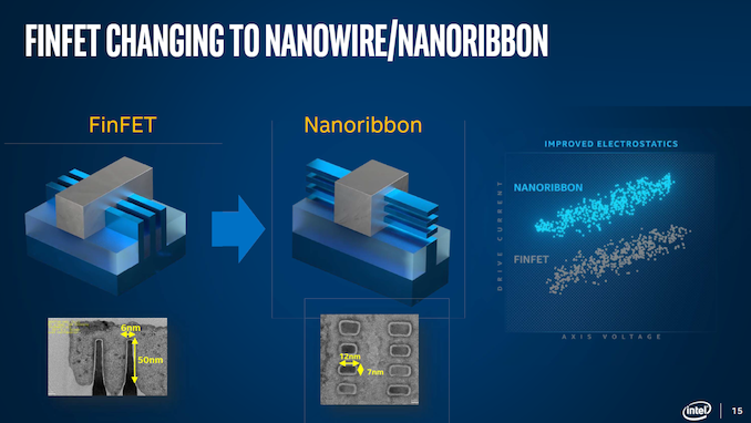
As expected, at some point the ability to scale a FinFET will become prohibitive, and new technologies will be needed to help continue the scaling. Research on post-FinFET transistor technology has been progressing at a break-neck pace, and most attention has been moved into ‘Gate-All-Around’ technology, which lifts the channel and allows the channel width to scale as needed for the type of transistor in use. GAA-FETs offer significant advantages when it comes to transistor performance control – for most FinFET processes, foundries can offer several designs based on voltage and performance, but GAA-FET designs turn those discrete options into something more continuous. You might see these referred to as nanosheets, or nanowires.


From Samsung


As is perhaps to be expected, GAA-FET designs (and layered GAA-FETs) are more complex to build than FinFETs or planar transistors. The first GAA-FET demonstration was in 1986, and in 2006 a 3nm implementation was demonstrated. However, building it in a lab compared to building it at scale as part of a foundry process available to customers is a different scale of complexity. At a number of technical semiconductor conferences through 2018 and 2019, a number of design companies and foundry offerings have discussed GAA-FET or similar designs as part of their upcoming portfolio.


Most notably, Intel has mentioned that they will start using it within the next 5 years, which would put it around its 5nm-3nm node technologies.


Intel


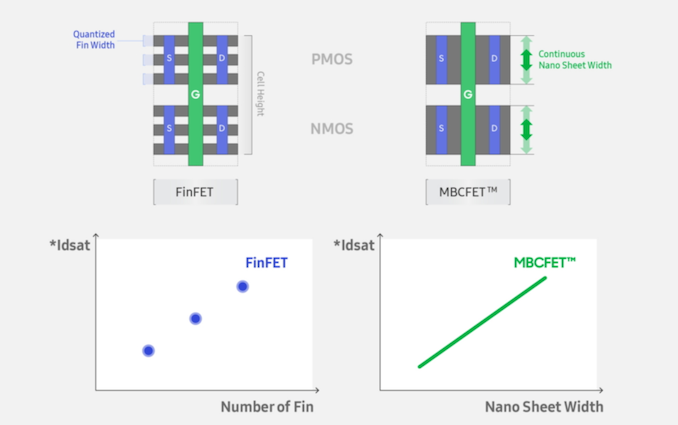
Samsung has announced its intention to deliver its version, known as MBC-FETs, as part of its 3nm process node, expected to be in volume manufacturing by late 2021. In May 2019, the company released a statement that the first v0.1 version of its 3GAE PDK was ready for customers. Over a year later, we would expect this to be on track – the 2020 version of Samsung’s Foundry Forum, which was delayed due to COVID, should be happening later this year.


Samsung


As these sorts of transistors grow in use, we expect the range of sheet widths available to increase, as well as the number of stacked layers in a GAA design. CEA-Leti this year, at the 2020 Symposia on VLSI Technology and Circuits, demonstrated a 7-layer GAA-FET using nanosheets specifically for high-performance computing.
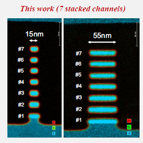


CEA-Leti


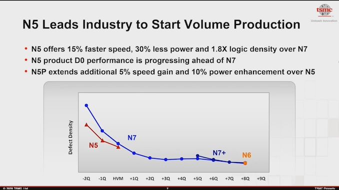
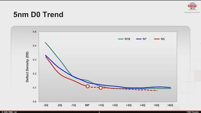
So what has happened with TSMC? As part of the Technology Symposium, it has stated that for its 3nm process technology it will remain with FinFETs. The company states that it has enabled a significant update to its FinFET technology to allow performance and leakage scaling through another iteration of its process node technology. TSMC’s N3 will use an extended and improved version on FinFET in order to extract additional PPA – up to 50% performance gain, up to 30% power reduction, and 1.7x density gain over N5. TSMC stated the predictability of FinFETs will help enable the company deliver the technology on an approved timescale.


This last statement is more than telling – if the development of FinFETs, now on its 3rd/4th/5th generation (depending on the foundry), has enabled a level of comfort and predictability that a first generation of GAA-FET cannot provide, then in order to satisfy its big customers (almost all leading-edge logic silicon), it has to keep to its cadence. That being said, there could be a chance for TSMC to offer GAA-FETs on different versions of its 3nm nodes in the future if it wishes, however the company has not made any public statements at this time to this effect, compared to Intel and Samsung.


As always with these technologies, the goal is to scale and bring some reality to wherever Moore’s Law is going. TSMC’s customers will have to wait until later to see if GAA-FETs can bring a more optimized flavor of performance to the table.


Related Reading


Source: AnandTech – Where are my GAA-FETs? TSMC to Stay with FinFET for 3nm

Nimbus Data’s New ExaDrive NL: 64 TB of Enterprise Grade QLC in 3.5-inch

Today Nimbus Data, one of the first companies to venture into enterprise flash storage in 2003, is announcing its latest generation ExaDrive product. Following on from the success of the 100 TB ExaDrive DC, the company is releasing a new ExaDrive NL series, from 16 TB to 64 TB. This new series uses enterprise grade QLC, compared to TLC in the DC variant, to provide a more cost effective solution with endurance designed to eclipses any other QLC drive on the market.


Source: AnandTech – Nimbus Data’s New ExaDrive NL: 64 TB of Enterprise Grade QLC in 3.5-inch

NVIDIA Confirms 12-pin GPU Power Connector

Today as part of a video showcasing NVIDIA’s mechanical and industrial design of its GPUs, and how it gets a large GPU to dissipate heat, the company went into some detail about how it needed to improve the design of all mechanical and electrical aspects of the board to aid cooling. This means implementing leaf springs for a back plate solution, as well as vapor chamber technology and using the right sorts of fans and fan management software.


As part of this video showcase, the company also shows its new 12-pin power connector. It also shows the 12-pin connector running perpendicular to the PCB, which is very interesting indeed.


Users who follow the tech news may have seen a few posts circling the internet regarding this 12-pin power connector, with a Seasonic cable that puts together two of the standard PCIe 8-pin connectors into one of NVIDIA’s new 12-pin designs.


Image from Hardwareluxx


NVIDIA states in the video that this 12-pin design is of its own creation. It isn’t clear if this is set to become a new standard in power cable connectivity for power supplies, however going forward we assume that most graphics cards that have this 12-pin power design will have to come with an additional 2×8-pin to 12-pin power cable included. We wait to see if that’s the case, or if it will be up to future power supplies to bundle the appropriate connector.


More details about the connector are expected to appear on September 1st during NVIDIA’s GeForce Special Event.


Related Links


Source: AnandTech – NVIDIA Confirms 12-pin GPU Power Connector

ASUS Announces ZenFone 7 Series: The Triple-Flip Camera – Hands-On

Today ASUS is announcing its follow-up to its innovative flip-camera design that was first introduced last year with the ZenFone 6. This year’s ZenFone 7 series, consisting of the regular ZenFone 7 and the ZenFone 7 Pro are sticking to the quite well received and innovative flip-camera design, improving upon its specification by adding in an extra camera module. We’ve also seen key specification improvements on the part of the phone itself, with an important shift from an LCD screen to a new 90Hz AMOLED display, as well as adoption of Qualcomm’s newest Snapdragon 865 and 865+ chipsets.


Source: AnandTech – ASUS Announces ZenFone 7 Series: The Triple-Flip Camera – Hands-On

2023 Interposers: TSMC Hints at 3400mm2 + 12x HBM in one Package

High-performance computing chip designs have been pushing the ultra-high-end packaging technologies to their limits in the recent years. A solution to the need for extreme bandwidth requirements in the industry has been the shifts towards large designs integrated into silicon interposers, directly connected to high-bandwidth-memory (HBM) stacks.


TSMC has been evolving their CoWoS-S packaging technology over the years, enabling designers to create bigger and beefier designs with bigger logic dies, and more and more HBM stacks. One limitation for such complex designs has been the reticle limit of lithography tools.


Recently, TSMC has been increasing their interpose size limitation, going from 1.5x to 2x to even projected 3x reticle sizes with up to 8 HBM stacks for 2021 products.


As part of TSMC’s 2020 Technology Symposium, the company has now teased further evolution of the technology, projecting 4x reticle size interposers in 2023, housing a total of up to 12 HBM stacks.


Although by 2023 we’re sure to have much faster HBM memory, a 12-stack implementation with the currently fastest HBM2E Samsung Flashbolt 3200MT/s modules would represent at least 4.92TB/s of memory bandwidth, which is multitudes faster than even the most complex designs today.


Carousel image credit: NEC SX-Aurora TSUBASA with 6 HBM2 Stacks


Related Reading


Source: AnandTech – 2023 Interposers: TSMC Hints at 3400mm2 + 12x HBM in one Package

TSMC Expects 5nm to be 11% of 2020 Wafer Production (sub 16nm)

One of the measures of how quickly a new process node gains traction is by comparing how many wafers are in production, especially as that new process node goes through risk production and then into high volume manufacturing. You can tell a lot about how much confidence a foundry has in its new process by looking at the number of wafers in production, as well as the expected range of customers and products that are set to be produced. As part of TSMC’s Technology Symposium 2020, we were treated to a little insight into the growth of its new 5nm process technology.


TSMC’s 5nm process, or strictly speaking its first production version of 5nm, known as N5, is currently in the process of high volume manufacturing. We are expecting the first consumer products that use N5 processors, particularly smartphones, out by the end of the year. That means that the companies who are building those products have already worked with pre-production silicon for validation, put their orders in for N5 parts, and may already be getting the first deliveries of the new hardware.


With such a new process, we always expect that initial production, even in ‘high volume production’ mode, is usually slow. This is due to product development, but also extensive validation and to make sure that the product isn’t a dud (such as TSMC’s ill-fated 20nm process). However, judging by the slides produced by TSMC at its Technology Symposium, it looks like that 11% of its 2020 production of 16nm+ wafers will be on 5nm.


It should be noted that this graph has ’12-inch wafer equivalents’ as the y-axis, which means that if any process node would use 8-inch wafers, it would be scaled accordingly. However, all of these leading edge process nodes are likely to be on 12-inch wafers.


Unfortunately there’s no real sense of how many wafers that is. TSMC has stated in another slide that it produced over 12 million 12-inch wafer equivalents in 2019, but that covers all processes and all facilities. At financial disclosures, TSMC does a breakdown of each node, but only in terms of revenue.


However, comparing 5nm to TSMC’s 7nm capability, it does show that 2019 to 2020, 7nm increased by 22.7%, and in 2020, 5nm production will be ~24% of 7nm production. This leads into TSMC’s narrative that it expects to grow its 5nm production to double in 2021, and triple in 2022, using the 2020 numbers as a base.


TSMC did give some insight into its 5nm manufacturing facilities also.


All of TSMC’s 5nm chips are being built at TSMC’s Fab 18, the newest fabrication plant that spreads over six buildings, which TSMC calls its ‘fourth GigaFab’. Fab 18 broke ground on January 26th 2018, and a year later the company started installing over 1300 manufacturing tools, including EUV machines, in a process that only took 8 months. From there, the company started testing its 5nm risk production, and started high-volume manufacturing in Q2. TSMC states that Fab 18 is capable of producing over one million 12-inch wafers per year, all on 5nm, and claims it leads the industry in energy efficiency for a fab of it size.


Related Reading


Source: AnandTech – TSMC Expects 5nm to be 11% of 2020 Wafer Production (sub 16nm)

TSMC’s Version of EMIB is ‘LSI’: Currently in Pre-Qualification

Whilst process node technologies and Moore’s Law are slowing down, manufacturers and chip designers are looking to new creative solutions to further enable device and performance scaling. Advanced packaging technologies are one such area where we’ve seen tremendous innovations over the past few years, such as the introduction of silicon interposers and integration of HBM-memory or the shift towards modularisation through chiplet designs.

Silicon interposers pose cost challenges as they are expensive and require quite a large silicon footprint, whilst chiplet designs which use conventional packaging on organic substrates are limited by I/O bandwidth and power efficiency. A solution to this problem has been the industry’s introduction of intermediary silicon dies that connect two logic chips together – but only in a limited scope, not using the same footprint as a full silicon interposer. Intel’s EMIB (Embedded Die Interconnect Bridge) has been the recently most talked about implementation of such technology.


Source: AnandTech – TSMC’s Version of EMIB is ‘LSI’: Currently in Pre-Qualification

TSMC Teases 12-High 3D Stacked Silicon: SoIC Goes Extreme

I’ve maintained for a couple of years now that the future battleground when it comes to next-generation silicon is going to be in the interconnect – implicitly this relies on a very strong catalogue of advanced packaging techniques in order to apply those interconnects and bring chips together. As we bring those chips closer together, elements such as power, thermals, and design complexity all get thrown into the mix, and it makes it very difficult to produce multi-connected products at high yield, moreso if they are stacked vertically rather than horizontally. This is why what TSMC showed at its Technology Symposium this week all the more crazy.


For some background, one set of technologies that TSMC has in its hand is SoIC: System on Integrated Chip. This is a key future TSMC integration technology that goes beyond past interposer or chip-stacking implementations, in that it allows stacking of silicon dies without the use of any µ-bumps at all, instead aligning and bonding the metal layers of the silicon directly to each other.


A single slide at the Technology Symposium shows it all off. TMSC is currently probing 12-Hi configurations of SoIC. Each of the dies within the 12-Hi stack has a series of through silicon vias (TSVs) in order for each layer to communicate with the rest of the layers, and the idea is that each layer could be a different element of logic, of IO, of SRAM, or could be passive to act as a thermal insulation layer between other active layers.


This design, as shown in the slide, has a maximum 600 micron thickness according to TSMC, which means that each layer is in the sub-50 micron level. Note that the bump pitch on a standard traditional die-stacking solution can be of the order of 50 microns. In the case of SoIC, the hybrid-bonding pitch is on the scale of 9µm for N7/N6 chips and 6µm for N5 chips. It shows that TSMC has some impressive linear manufacturing and wafer thinning technologies at hand in order to get this level of consistency and aligning of dies. The company has even demonstrated the capability to reduce this down to 0.9µm, a scale at which it would allow it to extend the back-end-of-line interconnect of a silicon chip.


The test chip shown in the slide is likely to be, if it is to showcase some initial runs, only 12 layers of passive silicon with basic TSV management. Obviously building something like this, thermals are going to come into play, but the main aspect here from TSMC’s point of view is that they can build it. It’s now up to the customers to book their place in line for the technology.


Carousel Image from Taiwan Semiconductor Manufacturing Co., Ltd.


Related Reading


Source: AnandTech – TSMC Teases 12-High 3D Stacked Silicon: SoIC Goes Extreme

be quiet! Announces Dark Power Pro 12 PSUs: 80Plus Titanium, Up to 1500W

The increasingly popular German hardware manufacturer be quiet! has announced its latest series in its ever-growing power supply line-up, the Dark Power Pro 12. Equipped with fully digital hardware and 80 PLUS Titanium certification, the be quiet! Dark Power Pro 12 power supplies will be available in capacities of 1200 and 1500 W with the ability to combine its multiple rails into one rail for overclocked processors and graphics cards.


According to be quiet!, the new Dark Power Pro 12 power supplies provide efficiency of up to 94.9%, which falls into the 80 PLUS Titanium certification range, with a fully digital design including the full bridge, LLC, SR, and DC/DC componentry. The Dark Power Pro 12 series builds upon the success of its previous 11 series with the use of its overclocking key, which combines the units six multiple rails into one rail for better stability when overclocking.


The be quiet! Dark Power Pro 12 series is using a full mesh PSU front for optimal airflow, with a 135 mm Silent Wings cooling fan designed to keep it cooled efficiently, but with less noise with a maximum dBA of 31.5 at 100% load for the 1500 W model, and just 25.8 dBA for the 1200 W model under the same conditions. Both the 1500 W and 1200 W models are the same size, with dimensions of 200 x 150 x 86 mm (L x W x H), and both share a fully-modular design with seventeen cables supplied with both units. All of be quiet!’s Dark Power Pro 12 power supplies come with a 10-year manufacturer’s warranty.


The Dark Power Pro 12 series will be available to purchase from the 8th September, with an MSRP of $449/£420/€439 for the 1500 W model, and $399/$370/€389 for the 1200 W variant.


Related Reading


Source: AnandTech – be quiet! Announces Dark Power Pro 12 PSUs: 80Plus Titanium, Up to 1500W

TSMC Updates on Node Availability Beyond Logic: Analog, HV, Sensors, RF

Most of the time when we speak about semiconductor processes, we are focused on the leading edge of what is possible. Almost exclusively that leading edge is designed for logic circuitry where performance and power efficiency are key drivers of pushing the boundaries, but also there’s a strong market in it. Other markets use semiconductor technology where there are other factors to consider: power, analog capabilities, voltage, and memory, all use semiconductor fabs but they are rarely at the leading edge. Nonetheless, the pureplay foundry businesses aims to offer enough technologies and features to cater as needed, along with driving which markets can use which technologies. At TSMC’s Technology Symposium this week, the company gave is a holistic view of its offerings.


Source: AnandTech – TSMC Updates on Node Availability Beyond Logic: Analog, HV, Sensors, RF

‘Better Yield on 5nm than 7nm’: TSMC Update on Defect Rates for N5

One of the key metrics on how well a semiconductor process is developing is looking at its quantitative chip yield – or rather, its defect density. A manufacturing process that has fewer defects per given unit area will produce more known good silicon than one that has more defects, and the goal of any foundry process is to minimize that defect rate over time. This will give the customers better throughput when making orders, and the foundry aims to balance that with the cost of improving the manufacturing process.


The measure used for defect density is the number of defects per square centimeter. Anything below 0.5/cm2 is usually a good metric, and we’ve seen TSMC pull some really interesting numbers, such as 0.09 defects per square centimetre on its N7 process node only three quarters after high volume manufacturing started, as was announced in November at the VLSI Symposium 2019. As it stands, the defect rate of a new process node is often compared to what the defect rate was for the previous node at the same time in development. As a result, we got this graph from TSMC’s Technology Symposium this week:


As it stands, the current N5 process from TSMC has a lower defect density than N7 did at the same time in its development cycle. TSMC. This slide from TSMC was showcased near the start of the event, and a more detailed graph was given later in the day:


This plot is linear, rather than the logarithmic curve of the first plot. This means that TSMC’s N5 process currently sits around 0.10 to 0.11 defects per square centimeter, and the company expects to go below 0.10 as high volume manufacturing ramps into next quarter.


Part of what makes 5nm yield slightly better is perhaps down to the increasing use of Extreme UltraViolet (EUV) technology, which reduces the total number of manufacturing steps. Each step is a potential chance to decrease yield, so my replacing 4 steps of DUV for 1 step of EUV, it eliminates some of that defect rate.


TSMC’s first 5nm process, called N5, is currently in high volume production. The first products built on N5 are expected to be smartphone processors for handsets due later this year.


Related Reading


Source: AnandTech – ‘Better Yield on 5nm than 7nm’: TSMC Update on Defect Rates for N5

Crucial Launches X6 Portable SSD, Updates X8 with 2TB Model: QLC Drives for the Budget-Conscious

Crucial introduced their first bus-powered direct-attached storage product last year – the X8 Portable SSD. The product put their P1 NVMe SSD behind an ASMedia bridge to offer read speeds of up to 1050 MBps. Only 500GB and 1TB capacities were launched. This refresh season sees a 2TB model being introduced in the X8 line. This is in addition to a new product that sacrifices the internal NVMe SSD for a SATA drive while retaining the USB 3.1 Gen 2 (10 Gbps) interface. This new product – the X6 Portable SSD – will be available in 1TB and 2TB capacities, with read speeds of up to 540 MBps.


Crucial doesn’t publicly state the type of NAND (QLC/TLC) inside either the X6 or X8. However, Crucial did officially confirm that their focus is on using the right type of NAND for the right consumer application. Quoting them verbatim: “The Crucial X6 is being positioned toward read-intensive workloads, and true-consumer applications. The product does not target high-end-content-creators who may benefit from TLC-memory characteristics.”


One doesn’t need to even read between the lines to determine that the X6 uses a QLC SSD internally. The X8 being based on P1 (Crucial’s first-generation QLC-based NVMe SSD) is also common knowledge. The company recently updated their BX500 entry-level SATA SSDs with 1TB and 2TB models. Eagle eyes might note that the lower capacities are 120GB, 240GB, and 480GB, while the older 960GB model has now been replaced with the 1TB version. Given that the BX500 initially launched with 64L 3D TLC, it makes sense that the 1TB and 2TB versions are 96L QLC drives. Based on the advertised bandwidth numbers, it is also very likely that the X6 Portable SSD internally uses the new BX500 QLC models.


Crucial touts the compact and lightweight nature (around 37g) as an attractive aspect for consumers. In order to cater to the budget-conscious, Crucial is keeping the package contents to the bare minimum – just the drive and a Type-C to Type-C cable. The Type-C to Type-A adapter is an additional part that costs around $10 more than the base package. The table below presents the pricing of the new products from Crucial, and a comparison with equivalent capacity offerings from Western Digital / SanDisk, and Samsung.


Portable SSDs Pricing – Crucial vs. Western Digital vs. Samsung
Crucial X6 Portable SSD 1TB ($155) WD My Passport SSD 2018 1TB ($169) Samsung T5 Portable SSD 1TB ($140)
SanDisk Extreme Portable SSD 1TB ($152)
Crucial X6 Portable SSD 2TB ($285) WD My Passport SSD 2018 2TB ($296) Samsung T5 Portable SSD 2TB ($280)
SanDisk Extreme Portable SSD 2TB ($290)
Crucial X8 Portable SSD 2TB ($330) WD My Passport SSD 2020 2TB ($380) Samsung T7 Portable SSD 2TB ($320)
SanDisk Extreme PRO Portable SSD 2TB ($348)

We reviewed the 1TB X8 Portable SSD earlier this year, and found that the drive significantly undercut the competition in terms of pricing. Since then, the competitors’ offerings have become cheaper. The trade-off between 3D TLC performance characteristics and QLC pricing becomes more of a challenge that has to be considered on a case-by-case basis. For the new products, despite the separation of the Type-C to Type-A adapter from the main package, the pricing gap has become quite narrow. As the above table shows, it is not even in favor of the QLC SSDs for certain capacity / performance points. Crucial will need to rethink pricing given the current state of the market.


Source: AnandTech – Crucial Launches X6 Portable SSD, Updates X8 with 2TB Model: QLC Drives for the Budget-Conscious

TSMC Details 3nm Process Technology: Full Node Scaling for 2H22 Volume Production

At TSMC’s annual Technology Symposium, the Taiwanese semiconductor manufacturer detailed characteristics of its future 3nm process node as well as laying out a roadmap for 5nm successors in the form of N5P and N4 process nodes.


Starting off with TSMC’s upcoming N5 process node which represents its 2nd generation deep-ultraviolet (DUV) and extreme-ultraviolet (EUV) process node after the rarely used N7+ node (Used by the Kirin 990 SoC for example). TSMC has been in mass production for several months now as we’re expecting silicon shipping to customers at this moment with consumer products shipping this year – Apple’s next-generation SoCs being the likely first candidates for the node.


TSMC details that N5 currently is progressing with defect densities one quarter ahead of N7, with the new node having better yields at the time of mass production than both their predecessor major nodes N7 and N10, with a projected defect density that’s supposed to continue to improve past the historic trends of the last two generations.


The foundry is preparing a new N5P node that’s based on the current N5 process that extends its performance and power efficiency with a 5% speed gain and a 10% power reduction.


Beyond N5P, TSMC is also introducing the N4 node that represents a further evolution from the N5 process, employing further EUV layers to reduce masks, with minimal migration work required by chip designers. We’ll be seeing N4 risk production start in 4Q21 for volume production later in 2022.


Today’s biggest news was TSMC’s disclosure on their next big leap past the N5 process node generation family, which is the 3nm N3 node. We’ve heard that TSMC had been working on defining the node back last year with progress going well.


Contrary to Samsung’s 3nm process node which makes use of GAA (Gate-all-around) transistor structures, TSMC will instead be sticking with FinFET transistors and relying on “innovative features” to enable them to achieve the full-node scaling that N3 promises to bring.


Advertised PPA Improvements of New Process Technologies
Data announced during conference calls, events, press briefings and press releases
  TSMC
N7

vs

16FF+
N7

vs

N10
N7P

vs

N7
N7+

vs

N7
N5

vs

N7
N5P

vs

N5
N3

vs

N5
Power -60% <-40% -10% -10% -30% -10% -25-30%
Performance +30% ? +7% +7% +15% +5% +10-15%
Logic Area


Reduction %


(Density)


70%


>37%


~17%


~17%

0.55x


-45%


(1.8x)


0.58x


-42%


(1.7x)

Compared to it’s N5 node, N3 promises to improve performance by 10-15% at the same power levels, or reduce power by 25-30% at the same transistor speeds. Furthermore, TSMC promises a logic area density improvement of 1.7x, meaning that we’ll see a 0.58x scaling factor between N5 and N3 logic. This aggressive shrink doesn’t directly translate to all structures, as SRAM density is disclosed at only getting a 20% improvement which would mean a 0.8x scaling factor, and analog structures scaling even worse at 1.1x the density.


Modern chip designs are very SRAM-heavy with a rule-of-thumb ratio of 70/30 SRAM to logic ratio, so on a chip level the expected die shrink would only be ~26% or less.


N3 is planned to enter risk production in 2021 and enter volume production in 2H22. TSMC’s disclosed process characteristics on N3 would track closely with Samsung’s disclosures on 3GAE in terms of power and performance, but would lead more considerably in terms of density.


We’ll be posting more detailed content from TSMC’s Technology Symposium in due course, so please stay tuned for more information and updates.


Related Reading:


Source: AnandTech – TSMC Details 3nm Process Technology: Full Node Scaling for 2H22 Volume Production

Intel Moving to Chiplets: ‘Client 2.0’ for 7nm

One of the more esoteric elements of Intel’s Architecture Day 2020 came very near the end, where Intel spent a few minutes discussing what it believes is the future of some of its products. Brijesh Tripathi, VP and CTO of Intel’s Client Computing group, laid out a vision about the future of its client products in the 2024+ future timeframe. Centered around Intel’s 7+ manufacturing process, the goal was to enable ‘Client 2.0’ – a new way to deliver and enable immersive experiences through a more optimized silicon development strategy.


Source: AnandTech – Intel Moving to Chiplets: ‘Client 2.0’ for 7nm

ASRock B550 Taichi Review: The $300 B550 Motherboard with Chutzpah

Outside of its Aqua series of motherboards, which come with exquisitely crafted monoblocks, ASRock’s Taichi brand has been a critical part of the company’s offerings in the land of premium motherboards. The ASRock B550 Taichi sits at the top of its product stack and features an impressive quality feature set. Some of the most notable features include a large 16-phase power delivery, eight SATA ports, dual M.2 slots, an Intel 2.5 GbE Ethernet controller, and an Intel Wi-Fi 6 interface. At $300 it comes equal in price with the X570 version, which leaves questions on the table as to which one is actually worth the money.


Source: AnandTech – ASRock B550 Taichi Review: The 0 B550 Motherboard with Chutzpah

Intel’s New 224G PAM4 Transceivers

One battleground in the world of FPGAs is the transceiver – the ability to bring in (or push out) high speed signals onto an FPGA at low power. In a world where FPGAs offer the ultimate ability in re-programmable logic, having multiple transceivers to bring in the bandwidth is a key part of design. This is why SmartNICs and dense server-to-server interconnect topologies all rely on FPGAs for initial deployment and adaptation, before perhaps moving to an ASIC. As a result, the key FPGA companies that play in this space often look at high-speed transceiver adoption and design as part of the product portfolio.


In recent memory, Xilinx and Altera (now Intel), have been going back and forth, talking about 26G transceivers, 28G transceivers, 56G/58G, and we were given a glimpse into the 116G transceivers that Intel will implement as an option for its M-Series 10nm Agilex FPGAs back at Arch Day 2018. The Ethernet based 116G ‘F-Tile’ is a separate chiplet module connected to the central Agilex FPGA through an Embedded Multi-Die Interconnect Bridge (EMIB), as it is built on a different process to the main FPGA.


As part of Intel’s Architecture Day 2020, the company announced that it is now working on a new higher speed module, rated at 224G. This module is set to support both 224G in a PAM4 mode (4-bits) and 112G in an NRZ mode (2-bits). This should enable future generations of the Ethernet protocol stack, and Intel says it will be ready in late 2021/2022 and will be backwards compatible with the Agilex hardened 100/200/400 GbE stack. Intel didn’t go into any detail about bit-error rates or power at this time, but did show a couple of fancy eye diagrams.


Related Reading


Source: AnandTech – Intel’s New 224G PAM4 Transceivers

Intel’s Future 7nm FPGAs To Use Foveros 3D Stacking

One of the main battlegrounds of future leading-edge semiconductor products will be in the packaging technology: being able to integrate multiple elements of silicon onto the same package with high bandwidth and low power interconnects will be, according to Intel, one way of extending the performance aspects of Moore’s Law into the next decade. Intel has three new parts to its advanced packaging portfolio: EMIB, Foveros, and ODI. At Intel’s Architecture Day 2020, we learned that Intel’s next generation of FPGA products, built on Intel’s own future 7nm manufacturing process, will integrate EMIB from its current generation as well as Foveros 3D stacking.


EMIB, or Embedded Multi-Die Interconnect Bridge, is essentially a bit of silicon embedded into a PCB substrate that allows a silicon die to connect to it in a very dense way. Two bits of silicon can connect to a single EMIB, allowing a fast and low power point-to-point interconnect. We have seen EMIB in use with Kaby Lake-G, the Stratix 10 GX 10M FPGAs, and for upcoming variations of Intel’s Xe graphics portfolio, such as Ponte Vecchio and Xe-HP. Intel has also released a royalty free version of EMIB, called AIB, which has its own generation-on-generation upgrade path for use in the wider industry.


Foveros is Intel’s die-to-die ‘3D’ stacking technology that allows two bits of silicon to connect on top of each other, again in a high-bandwidth and low power implementation. Foveros is currently in use in Intel’s Lakefield mobile processor, and has been announced for future products such as Ponte Vecchio. We now have another one to add to that list: FPGAs.


There is no distinct detail about what the next generation FPGAs would have, aside from Intel’s 7nm process and be stacked upon a base die that contains the HBM IO and DDR connections. I assume that the goal here is to have a common base die for a number of FPGA sizes, and then different variants of the 7nm FPGA could be stacked on top based on customer needs, or based on productization perhaps due to yield or cost or such. Technically Intel calls any product with both EMIB and Foveros a ‘Co-EMIB’ product, and this falls under that naming. One of the new elements that the 7nm FPGAs will have access to is a new 224G PAM4 transceiver module, which Intel is currently in the process of tuning and validating.


It is unclear exactly when these new 7nm FPGAs will be launched – Intel’s own slide decks show a roadmap where the current 10nm Agilex FPGAs are the main products for 2021/2022, so we are perhaps looking at 2023 or later for these designs. They are far enough out that Intel doesn’t have it on the following roadmap:


A word on ODI, or Omni-Directional Interconnect. When a chip is built with Foveros, the high-power compute chip often has to be on top for thermal reasons, but the power for that compute chip has to travel through the base chip to reach the compute one. It also means that the top chips are smaller than the ones underneath. ODI solves this issue, by allowing the top chip to ‘hang’ over the edge, in a cantilevered fashion, such that the power connections from the base substrate can rise up through directly to the compute die. If there are enough power connections, then these connections can also be high-bandwidth data connections. This has added benefits in signal integrity, but also added complications in manufacturing and layout.


We expect ODI to be used more in the small-die space first, perhaps in future generations of ‘Lakefield’ type designs, rather than in FPGAs.


Related Reading:


Source: AnandTech – Intel’s Future 7nm FPGAs To Use Foveros 3D Stacking

Cerebras Wafer Scale Engine News: DoE Supercomputer Gets 400,000 AI Cores

One of the more interesting AI silicon projects over the last couple of years has been the Cerebras Wafer Scale Engine, most notably for the fact that a single chip is the size of a literal wafer. Cerebras packs the WSE1 chip into a 15U custom liquid cooled server, called the CS-1, with a number of innovations regarding packaging, power, and setup. A single CS-1 requires about 20 kW of power peak, and costs around a couple million dollars (the Pittsburgh Supercomputing Center purchased two last year based on a $5m research grant). Cerebras say they have double digit customers and several dozen units already in the field, however today marks a considerable milestone as the US Department of Energy now has one deployed and working, attached directly to a supercomputer.


Source: AnandTech – Cerebras Wafer Scale Engine News: DoE Supercomputer Gets 400,000 AI Cores

Intel Xe-HP Graphics: Early Samples Offer 42+ TFLOPs of FP32 Performance

One of the promises that Intel has made with its new Xe GPU family is that in its various forms it will cater to uses ranging from integrated graphics all the way up to the high performance compute models needed for super-dense supercomputers. This means support for the types of calculations involved in simple graphics, complex graphics, ray tracing, AI inference, AI training, and the compute that goes into molecular modelling, oil-and-gas, nuclear reactors, rockets, nuclear rockets, and all the other big questions where more compute offers more capabilities. Sitting near the top of Intel’s offerings is the Xe-HP architecture, designed to offer high performance GPUs for standard server and enterprise deployments.


Source: AnandTech – Intel Xe-HP Graphics: Early Samples Offer 42+ TFLOPs of FP32 Performance