Schenker VIA 14: 14-inch Tiger Lake Magnesium Notebook, with 28W Version Inbound

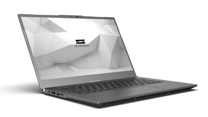
With Intel lifting the lid on its new Tiger Lake mobile processors today, a number of vendors are announcing their upcoming notebooks. Schenker Technologies, a German brand known in Europe for its Xtreme Mobile Gaming (XMG) line of products and custom Clevo implementations, is one of the first to describe an upcoming 11th Gen Intel Tiger Lake portable notebook as part of its VIA line. With a lightweight magnesium chassis, the VIA 14 uses up to a Core i7, a 73 Wh battery, and a one watt display to give 14+ hours of battery life.


The key thing to note about Tiger Lake is the increase in both CPU and GPU performance compared to the previous generation Intel notebook processors. We still have four cores, but the Tiger Lake cores can now boost a lot higher due to Intel’s improved 10nm SuperFin process (which you can read about here). Tiger Lake is Intel’s first product with its new Xe-LP graphics design as well, promising 2x the graphics performance of the last generation. The goal with these processors is to enable a nice and comfortable experience in a range of designs from ultra-premium to the run-of-the-mill.


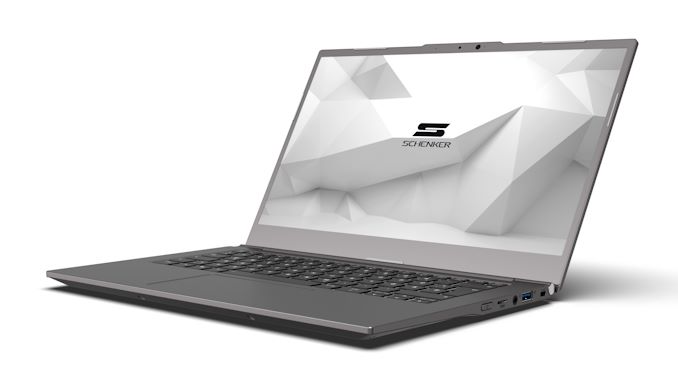
The Schenker VIA 14 sits in that ultra-premium market. Using a lightweight magnesium chassis, the kind that we only ever see on the expensive end of the market, the VIA 14 is claiming only a 1.1 kg (2.4 lbs) weight despite also putting a 73 Wh battery inside. Personally I find this a bit mind blowing, if I’m honest. A 73 watt-hour battery in a 1.1 kg notebook is insane, and they are also claiming a 90% charge in 90 minutes. Not only that, but there’s also one of Intel’s approved low-power one-watt displays, enabling 14+ hours of active battery life according to the press release when at 150 nits.


Tiger Lake also enables PCIe 4.0 storage, native Thunderbolt 4, and Schenker will also support an optional LTE modem for business customers. Despite being lightweight, the big battery means the notebook is 16.5 mm, but with a 14-inch display is still very portable. The ports with the VIA 14 include a HDMI 2.0b connection, a USB 4.0/Thunderbolt 4 Type-C with DisplayPort 1.4b support, two USB-A 3.2 ports, a microSD card reader and a combination headphone jack. Native connectivity is through Wi-Fi 6, and as mentioned, an LTE add-on is supported.


For storage, the VIA 14 has support for two M.2 SSDs, one at PCIe 4.0 and the other at PCIe 3.0. Memory is DDR4-3200, with 8 GB coming pre-soldered and an 8 GB SO-DIMM module coming as standard, however up to 40 GB total memory can be supported. The 14-inch display has a maximum brightness of 300 nits and provides 98% coverage – Schenker says the special ‘one-watt’ display applies when running at 150 nits. The display also opens to a 180-degree hinge.


Prices for the VIA 14 will start at €1,246.75 (that includes 16% VAT) at the end of October. The base model features the Core i7-1165G7, 8 GB DDR4, and a 250 GB Samsung 860 Evo SSD, and models with the Core i5-1135G7 will follow later.


Schenker also included a preview of what is to come, simply stating that a version with a 28 W Tiger Lake processor paired with an NVIDIA graphics card will be ‘coming soon’.


Related Reading


Source: AnandTech – Schenker VIA 14: 14-inch Tiger Lake Magnesium Notebook, with 28W Version Inbound

Intel Launches 11th Gen Core Tiger Lake: Up to 4.8 GHz at 50 W, 2x GPU with Xe, New Branding

In August, Intel ran one of its rare Architecture Days where the company went into some detail about its upcoming Tiger Lake processor. This included target markets, core counts, graphics counts, a look into some of the new acceleration features, and a promise of a product launch later in the year. That product launch is now here, and Intel is providing Tiger Lake with speeds and feeds, providing detail and expected benchmark performance for Intel’s next generation of notebook-class devices.


Source: AnandTech – Intel Launches 11th Gen Core Tiger Lake: Up to 4.8 GHz at 50 W, 2x GPU with Xe, New Branding

3DFabric: The Home for TSMC’s 2.5D and 3D Stacking Roadmap

Interposers. EMIB. Foveros. Die-to-die stacking. ODI. AIB.TSVs. All these words and acronyms have one overriding feature – they are all involved in how two bits of silicon physically connect to each other. At the simple level, two chips can be connected through the printed circuit board – this is cheap but doesn’t allow for great bandwidth. Above this simple implementation, there are a variety of ways to connect multiple chiplets together, and TSMC has a number of these technologies. In order to unify all the different names it gives to its variants of its 2.5D and 3D packaging, TSMC has introduced its new overriding brand: 3DFabric.


Source: AnandTech – 3DFabric: The Home for TSMC’s 2.5D and 3D Stacking Roadmap

TeamGroup Previews New 15.36 TB Consumer SATA SSD, for $3990

The two main angles that most SSD storage seems to be moving towards is performance or capacity. On the capacity front, we are starting to see the first 8 TB consumer drives coming to the market in a variety of formats. Always willing to jump ahead of the competition, TeamGroup has announced its new QX ‘Extra Large’ SSD coming in at 15.36 TB.


This new SSD is equipped with 3D QLC flash NAND, allowing it to hit the high capacity. The 2.5-inch drive has an SLC cache mode ahead of the DRAM buffer, which allows the drive to reach 560 MB/s reads and 480 MB/s writes according to the press release. The drive is rated under warranty for 2560 Terabytes Written, which comes down to 0.15 drive writes per day if the warranty is three years – TeamGroup has not specified any exact warranty at this time. At any rate, even with full sequential write speed, it would take around 60-70 days of continuous writes to go through that warranty.


Nothing else from TeamGroup’s press release seems out of the ordinary for a standard SATA SSD. We’ve reached out to ask exactly what SSD controller or NAND is under the hood, as these weren’t provided. There’s also no mention of IOPS. TeamGroup claims this drive is aimed at the consumer market, which it is only by virtue of it lacking a number of premium enterprise features. The price however is decidedly non-consumer: an eye-watering $3990 per drive, and the drives seem to be only made-to-order by OEM or SI clients. That’s $260 per TB of SATA SSD.


It’s worth noting that we discussed the NimbusData NL drive last week, which is also a high-capacity SATA SSD but geared up to the enterprise market. The 16 TB version of that drive is only $2900, a lot cheaper than this. The flip side of that is the 3.5-inch form factor of the NimbusData NL, compared to 2.5-inch (likely 15mm) for TeamGroup.


In the end, I’m of the opinion that TeamGroup is unlikely to sell many of these, except to niche customer bases, or laptop deployments perhaps – both of which are unlikely to be too keen on the ‘consumer’ designation.


Related Reading


Source: AnandTech – TeamGroup Previews New 15.36 TB Consumer SATA SSD, for 90

NVIDIA Announces the GeForce RTX 30 Series: Ampere For Gaming, Starting With RTX 3080 & RTX 3090

With much anticipation and more than a few leaks, NVIDIA this morning is announcing the next generation of video cards, the GeForce RTX 30 series. Based upon the gaming and graphics variant of NVIDIA’s Ampere architecture and built on an optimized version of Samsung’s 8nm process, NVIDIA is touting the new cards as delivering some of their greatest gains ever in gaming performance. All the while, the latest generation of GeForce will also be coming with some new features to further set the cards apart from and ahead of NVIDIA’s Turing-based RTX 20 series.

Out of the gate, NVIDIA is announcing the first three cards to make up the new RTX 30 series: the RTX 3090, RTX 3080, and RTX 3070. These cards are all launching within the next month and a half – albeit at slightly separate times – with the RTX 3090 and RTX 3080 leading the charge. The two cards, in turn, will serve as the successors to NVIDIA’s GeForce RTX 2080 Ti and RTX 2080/2080S respectively, hitting new highs in graphics performance, albeit while also hitting new highs in prices in the case of the RTX 3090.

The first card out the door will be the GeForce RTX 3080. With NVIDIA touting upwards of 2x the performance of the RTX 2080, this card will go on sale on September 17th for $700. That will be followed up a week later by the even more powerful GeFoce RTX 3090, which hits the shelves September 24th for $1500. Finally, the RTX 3070, which is being positioned as more of a traditional sweet spot card, will arrive next month at $499.


Source: AnandTech – NVIDIA Announces the GeForce RTX 30 Series: Ampere For Gaming, Starting With RTX 3080 & RTX 3090

The NVIDIA GeForce Special Event 2020 Live Blog (Starts at 9:00 PT/16:00 UTC)

With much anticipation and more than a few leaks, today is NVIDIA’s 2020 GeForce Special event. We’re expecting the announcement of NVIDIA’s GeForce RTX 30 series of cards, based on their Ampere architecture, and with it a generational improvement in performance. So please join us for the event, which starts at 9am Pacific, 16:00 UTC.


Source: AnandTech – The NVIDIA GeForce Special Event 2020 Live Blog (Starts at 9:00 PT/16:00 UTC)

Seagate Updates IronWolf NAS Drives Lineup with 18TB Pro HDD and New 4TB SSDs

Seagate is introducing new flagships in their IronWolf lineup today on two fronts – the SMB/SME-focused IronWolf Pro, and the SATA SSDs line. On the HDD front, we have 18TB hard drives based on conventional magnetic recording (CMR) technology, while the SATA SSD line sees two new SKU sets – the IronWolf 125 and the IronWolf Pro 125 (joining the current IronWolf 110 and the NVMe-based IronWolf 510).


Given the premium nature of the 18TB capacity point, Seagate is launching the capacity only in the IronWolf Pro line (the vanilla IronWolf models top out at 16TB). The ST18000NE000 18TB Pro model is compatible with NAS units of up to 24 bays, and has a workload rating of 300TB/yr. It is a 7200 rpm 9-platter helium-filled drive, with a DRAM cache of 256MB (which seems to be half of what is offered by Western Digital in their Gold line of enterprise hard drives – the other 18TB choice in the retail market). The drive comes with a 5-year warranty and is rated for 24×7 operation, with a MTTF of 1.2M hours.


The average power consumption sees an increase from 7.6W for the 16TB model to 8W for the 18TB version. The drive does use TDMR technology for the heads, and we have reached out to Seagate for information on possible HAMR usage.


The new SATA SSDs are 2.5″ drives with different optimizations for varying use-cases. The IronWolf 125 is meant as a capacity play – available in capacities ranging from 250GB all the way to 4TB. It comes with a 0.7DWPD rating, and no power-loss protection. On the other hand, the IronWolf Pro 125 has a 1DWPD rating, more over-provisioning (rated capacities range from 240GB to 3.84TB), and comes with power-loss protection. The Pro drives come with a 2M hour MTTF, while the corresponding metric is 1.8M hours for the non-Pro version. Both drives come with a 5-year warranty, with the Pro series including a 3-year data recovery service.


<!–


–>


<!–


–>


The Seagate IronWolf 125 SSDs for NAS
Capacity 250 GB 500 GB 1 TB 2 TB 4 TB
Model Number ZA2500NM10002 ZA500NM10002 ZA1000NM10002 ZA2000NM10002 ZA4000NM10002
Controller ?
NAND Flash 3D TLC NAND
Form-Factor, Interface 2.5″ x 7mm, SATA III 6 Gbps
Seq. Read (128KB @ QD32) 560 MBps 2450 MBps 2650 MBps 3150 MBps
Seq. Write (128KB @ QD32) 540 MBps
Rand. Read IOPS (QD32T8) 95K
Rand. Write IOPS (QD32T8) ?
Pseudo-SLC Caching ?
DRAM Buffer ?
TCG Opal Encryption ?
Power Consumption Avg Active 2.3 W 2.4 W 2.6 W 2.8 W
Avg Idle 0.11 W 0.115 W 0.13 W 0.14 W
Warranty 5 years
MTBF 1.8 million hours
TBW 300 700 1400 2800 5600
DWPD 0.7
UBER 1E10^17
Additional Information Link
MSRP $63 $84 $142 $294 $609


<!–


–>


The Seagate IronWolf Pro 125 SSDs for NAS
Capacity 240 GB 480 GB 960 GB 1920 GB 3840 GB
Model Number ZA240NX10001 ZA480NX10001 ZA960NX10001 ZA1920NX10001 ZA3840NX10001
Controller ?
NAND Flash 3D TLC NAND
Form-Factor, Interface 2.5″ x 7mm, SATA III 6 Gbps
Seq. Read (128KB @ QD32) 545 MBps
Seq. Write (128KB @ QD32) 360 MBps 500 MBps 520 MBps
Rand. Read IOPS (QD32T8) 90K 96K
Rand. Write IOPS (QD32T8) 12K 16K 25K 30K
Pseudo-SLC Caching ?
DRAM Buffer ?
TCG Opal Encryption ?
Power Consumption Avg Active 2.5 W 3 W 4 W 4.4 W 5 W
Avg Idle 1.4 W 1.6 W 1.8 W 1.9 W
Warranty 5 years (including 3 years of Rescue Data Recovery Services)
MTBF 2 million hours
TBW 435 875 1750 3500 7000
DWPD 1
UBER 1E10^17
Additional Information Link
MSRP $98 $146 $264 $474 $888

The new IronWolf Pro 18TB HDD is priced at $609 (compared to $593 for the equivalent WD Gold drive). Pricing for the different models in the IronWolf (Pro) 125 SSD series is available in the tables above. The main competition here is Western Digital’s WD Red SA500 series. Seagate does more product segmentation / firmware tweaking for the NAS SSD market, allowing consumers to choose a SSD tuned for their requirements.


Source: AnandTech – Seagate Updates IronWolf NAS Drives Lineup with 18TB Pro HDD and New 4TB SSDs

Samsung Launches New Galaxy Z Fold2 at $1999

Samsung’s new Galaxy Z Fold2 had been originally announced several weeks ago alongside the Note20 series, however the company had been delaying the official launch of the phone until September. Well, September has now come and Samsung is now ready to fully unveil the specifications of the new flagship foldable phone and finally starting to take pre-orders.


The new iteration is an important generational evolution over last year’s problem-ridden Galaxy Fold, promising to notably improve some of the key weaknesses of the first design.


Samsung Galaxy Folds
  Galaxy Z Fold2 Galaxy Fold
SoC Qualcomm Snapdragon 865+

1x Cortex A77 @ 3.1GHz

3x Cortex A77 @ 2.42GHz

4x Cortex A55 @ 1.80GHz


Adreno 650 @ 670MHz

Qualcomm Snapdragon 855 

1x Kryo 485 (CA76) @ 2.84GHz

3x Kryo 485 (CA76) @ 2.42GHz

4x Kryo 485 (CA55) @ 1.80GHz


Adreno 640

Display Main Display:

7.6″ 2208 x 1768

Foldable Dynamic AMOLED (11.25:9)

Cover display:

6.2″ 2260 x 816

AMOLED (25:9)

Main Display:


7.3″ 2048 x 1536

Foldable Dynamic AMOLED (4.2:3)

Cover display:


4.6″ 1680 x 720

Super AMOLED (21:9)

Dimensions Folded:

159.2 x 68.0 x 13.8 – 16.8mm

Unfolded:
159.2 x 128.2 x 6.0 – 6.9mm

282g

Folded:

160.9 x 62.8 x 15.7 – 17.1mm

Unfolded:

160.9 x 117.9 x 6.9mm

276g
RAM 12GB LPDDR5 12GB LPDDR4X
NAND 256GB UFS3.1 512GB UFS3.0
Battery 4500mAh  (17.41Wh) typ. 4380mAh  (16.86Wh)
Front Camera Cover & Front Cameras

(2x identical)


10MP 1.22μm
F2.2 FOV: 80˚

Cover Camera:

10MP f/2.2 “Selfie camera”

Front camera:

10MP f/1.9 4K video recording

Front camera:

8MP, f/2.2

Dual Pixel PDAF

Primary Rear Camera 83° Wide Angle
12MP 1.8µm Dual Pixel PDAF


f/1.8 w/ OIS

77° Wide Angle

12MP 1.4µm Dual Pixel PDAF


Adjustable aperture f/1.5 or f/2.4

Secondary Rear Camera 123° Ultra-Wide Angle
12MP 1.12µm f/2.2
123° Ultra-Wide Angle

16MP 1.0µm f/2.2
Tertiary Rear Camera 45° / Telephoto lens 2x zoom

12MP 1.0µm

f/2.4 w/OIS
SIM Size ??? NanoSIM
Wireless 802.11a/b/g/n/ac/ax 2×2 MU-MIMO,

BT 5.0 LE,

NFC, GPS/Glonass/Galileo/BDS
802.11a/b/g/n/ac 2×2 MU-MIMO,

BT 5.0 LE,

NFC, GPS/Glonass/Galileo/BDS
Connectivity USB Type-C USB Type-C
Features They both fold
Launch OS Android 10 Android 9.0
Launch Price $1999 $1980 / 2000€

From a specification standpoint, the new Z Fold2 updates its hardware to the newest Snapdragon 865+ from Qualcomm which we’ve seen in a lot of the recent smartphone releases this summer.


Samsung opted to keep the RAM steady at 12GB, and oddly enough we’ve seen a reduction in the storage department as the Z Fold2 comes with 256GB of UFS3.1 storage, half of the 512GB of the first Galaxy Fold.


Big upgrades include a new redesigned screen with a more robust and better functioning hinge mechanism. The new display grows to 6.7” diagonal when unfolded, reaching a new 2208 x 1768 resolution.


Samsung here did away with the big corner notch with the multiple front cameras, instead opting for a hole-punch camera in the right half of the internal screen. The camera module here is a 10MP unit with 1.22µm pixels and f/2.2 optics.


A bigger display upgrade has been made on the cover display side of the phone, as the new screen grows from 4.6” to 6.2”, with much less bezel surrounding it. It’s a big change in the looks of the phone and makes the cover display significantly more usable. Samsung here also opted for a hole-punch camera at the top centre of the panel, with an identical 10MP module as the internal front camera.


In terms of the primary rear-facing cameras, the main unit has seen an upgrade to an identical module as found in the Galaxy S20 with a 12MP f/1.76” sensor with 1.8µm pixels and an f/1.8 optics with OIS.


The ultra-wide is a bit different than the original Fold in that it reduces its resolution from 16Mp to 12MP, but retains the same sensor size – it’s not the same unit as on the S20 and Note20 series. We still see a super-wide 123° field-of-view with an f/2.2 aperture.


The telephoto unit has 2x optical magnification and seems to be a continuation of the unit we’ve seen on the original Fold, with a 12MP 1.0µm sensor and f/2.4 optics with OIS.


Samsung promises various new software improvements this generation, making for a more seamless experience between the different displays, as well as having extensive optimisations for simultaneous multi-tasking with multiple open apps at once.


The new Galaxy Z Fold2 is now open for pre-orders starting September 2nd at a launch price of $1999, with general availability starting September 25th.


Related Reading:


Source: AnandTech – Samsung Launches New Galaxy Z Fold2 at 99

HP Updates The ZBook Lineup With Power And Fury

Today HP is launching updates to their ZBook lineup with the new HP ZBook Fury 15 and 17, and the ZBook Power G7 mobile workstations offering performance, manageability, and a more compact footprint than the outgoing generation of ZBooks. Both are available with the latest Comet Lake H Series processors, as well as a Xeon variant and ECC memory, as well as NVIDIA Quadro GPUs.


HP ZBook Lineup 2020
  Fury 15 Fury 17 Power G7
CPU Intel Core i5-10300H 4-Core 2.5-4.5 GHz

Intel Core i5-10400H 4-Core 2.6-4.6 GHz vPro

Intel Core i7-10750H 6-Core 2.6-5.0 GHz

Intel Core i7-10850H 6-Core 2.7-5.1 GHz vPro

Intel Core i9-10885H 8-Core 2.5-5.3 GHz vPro

Intel Xeon W-10855M 6-Core 2.8-5.1 GHz ECC vPro
GPU Intel UHD Graphics
NVIDIA Quadro:

RTX 5000 16GB GDDR6

RTX 4000 8GB GDDR6

RTX 3000 6GB GDDR6

T2000 4GB GDDR6

T1000 4GB GDDR6

AMD:

Radeon Pro W5500M 4GB GDDR6

Radeon RX5500M 4GB GDDR6

Intel UHD Graphics
NVIDIA Quadro:

RTX 5000 Max-Q 16GB GDDR6

RTX 4000 Max-Q 8GB GDDR6

RTX 3000 6GB GDDR6

T2000 Max-Q 4GB GDDR6

T1000 Max-Q 4GB GDDR6

AMD:

Radeon Pro W5500M 4GB GDDR6

Radeon RX5500M 4GB GDDR6

Intel UHD Graphics
NVIDIA Quadro:

T2000 4GB GDDR6

T1000 4GB GDDR6

T620 4GB GDDR6
RAM 4 SODIMM Slots

128 GB DDR4-2667 Max Non-ECC

64 GB DDR4-2667 Max ECC
2 SODIMM Slots

64 GB DDR4-3200 Max Non-ECC

32 GB DDR4-2667 Max ECC
Storage 2 x M.2 Slot

4 TB SSD Max

1 x 2.5″ SATA

2 TB 5400 rpm max
1 x M.2 slot

2 TB SSD Max
Display 15.6-inch Display

1920×1080 IPS 250 Nit 45% NTSC

1920×1080 IPS 400 Nit 72% NTSC

1920×1080 IPS 1000 nit 72% NTSC HP SureView Privacy screen

3840×2160 IPS Touch 600 Nit 100% P3

3840×2160 IPS 600 Nit 100% P3 HP Dreamcolor
17.3-inch Display

1920×1080 300 Nit 72% sRGB

3840×2160 IPS 550 Nit 100% P3

3840×2160 550 Nit 100% P3 Anti-Glare

3840×2160 IPS 550 Nit 100% P3 HP Dreamcolor
15.6-inch Display

1920×1080 IPS 250 Nit 45% NTSC

1920×1080 IPS 400 Nit 100% sRGB low-power

3840×2160 IPS Touch 400 Nit 100% sRGB low-power

1920×1080 IPS 250 Nit 45% NTSC Touch
Networking Intel I219 Gigabit Ethernet

Intel Wi-Fi 6 AX201

Intel 7360 LTE Modem
Intel I219 Gigabit Ethernet

Intel Wi-Fi 6 AX201
Expansion Left Side:

1 x RJ-45

1 x USB 3.1 Gen1 Charging

1 x USB 3.1 Gen1

Headset jack

Right Side:

1 x power

1 x Mini DisplayPort 1.4

1 x HDMI 2.0b

2 x Thunderbolt 3 Type-C port
Left Side:

1 x HDMI 2.0< br />1 x RJ-45

1 x USB 3.1 Gen1 Charging

Right Side:

1 x Power

2 x USB 3.1 Gen1

1 x Headset jack< br />1 x Thunderbolt 3 Type-C
Camera 720p HD Camera, 720p HD IR Camera
Battery 94 Wh Li-ion

120W/150W/200W AC Adapters depening on GPU
83 Wh Li-Ion

120W/150W AC Adapter depending on GPU
OS Windows 10 Pro

Windows 10 Pro for Workstations

Windows 10 Home

FreeDOS 3.0

Red Hat Enterprise Linux 8
Windows 10 Pro

Windows 10 Pro for Workstations

Windows 10 Home

FreeDOS 3.0
Dimensions 357 x 242.5 x 25.9 mm

14.06 x 9.55 x 1.05 inches
398.4 x 267.1 x 26.9 mm

15.69 x 10.52 x 1.06 inches
359.4 x 233.9 x 28.6 mm

14.15 x 9.21 x 0.9 inches
Starting Weight 2.42 Kg / 5.32 lbs 2.97 Kg / 6.53 lbs 1.92 Kg / 4.32 lbs
Available Sept 14 2020 Oct 5 2020

HP ZBook Fury 15 and Fury 17


If you need the most performant ZBook around, look no further than HP’s Fury lineup, which features both a 15.6-inch and 17.3-inch variant. The Fury 15 is 12% smaller than the previous generation, and the Fury 17 is 29% smaller, but both still pack a punch with Intel Core i5, i7, i9, and Xeon options with up to 5.3 GHz. The Xeon adds in ECC memory support, and HP has outfitted the laptops with 4 SODIMM slots for up to 128 GB of DDR4 non ECC RAM, or 64 GB of ECC. HP offers up to 10 TB of storage as well with dual M.2 slots with 4 TB max each, and a 2.5” SATA drive with 2 TB.


HP is offering 1920×1080 IPS displays as a base offering on both models, with the Fury 15 having an available privacy screen. Both the Fury 15 and Fury 17 also have UHD display options, with 100% P3 gamut support and an optional 10-bit HP DreamColor panel.


To drive the displays, HP offers what feels like every mobile workstation GPU available, so you can basically pick what fits your needs based on application support, performance, and of course cost. On the NVIDIA side there is Quadro RTX 5000, 4000, and 3000. If you do not need the tensor cores, there are also Quadro T2000 and T1000 GPUs available. If you would prefer an AMD GPU, HP offers the Radeon Pro W5500M and Radeon RX 5500M. There is something for everyone.


Being a mobile workstation, there is of course Thunderbolt 3 support, and plenty of connectivity options. For networking, clients can utilize the included Gigabit Ethernet, or Wi-FI 6 based on the Intel AX201, and if you are on the go, HP offers LTE as well with the Intel 7360 LTE modem.


HP will be offering the new Fury 15 and Fury 17 on September 14 at HP.com.


HP ZBook Power G7


HP is also offering the new ZBook Power G7, which offers much of the same features as a typical ZBook with a MIL-STD chassis, manageability, and support, but at a more affordable price point. The Power G7 still offers the same range or processor options as the Fury models, but the 15.6-inch laptop is smaller, lighter, and not available with the high-performance Quadro RTX GPUs, but is instead limited to the Quadro T2000, T1000, or T620 GPU.


Storage and RAM maximums are also lower, due to the smaller chassis, with only two SODIMM slots instead of 4 on the Fury series, meaning RAM is maxed out at 64 GB of non-ECC, or 32 GB of ECC RAM. There is a single M.2 slot, which HP offers up to 2 TB of storage with.


As with the Fury 15, the Power G7 offers a 15.6-inch display with a 1920×1080 base configuration, and optional UHD, but the display sticks to the sRGB color space.


There is still Thunderbolt 3 support, as well as Gigabit Ethernet, and Wi-Fi 6, but no cellular option on this model.


For some though, the lower power and therefore reduced weight will be a bonus, with the Power G7 starting weight a full pound lighter than the Fury 15, at 4.32 lbs. It’s not an ultralight 15-inch laptop, but still hits a good starting weight despite the ability to pack in a Xeon processor.


The HP ZBook Power G7 should be available on October 5 at HP.com.


Source: AnandTech – HP Updates The ZBook Lineup With Power And Fury

The ASUS ZenFone 7 Pro Review: The Triple Flip-Camera

ASUS last week released the brand new ZenFone 7 and ZenFone 7 Pro series, and today’s we’re ready to publish our testing of the company’s newest “mainsteam” flagship device.

This year’s ZenFone 7 series, consisting of the regular ZenFone 7 and the ZenFone 7 Pro are sticking to the quite well received and innovative flip-camera design, improving upon its specification by adding in an extra camera module. We’ve also seen key specification improvements on the part of the phone itself, with an important shift from an LCD screen to a new 90Hz AMOLED display, as well as adoption of Qualcomm’s newest Snapdragon 865 and 865+ chipsets.

This year, the company is also releasing two variants of the phone – beyond higher DRAM and storage configurations, the higher-end model features a higher-binned SoC as well as differentiates the camera systems by exclusively employing OIS – which is an interesting way to segment things.


Source: AnandTech – The ASUS ZenFone 7 Pro Review: The Triple Flip-Camera

Toshiba Updates Canvio Portable Storage Lineup with Flex and Gaming HDDs

Hard disk drives still rule the roost when dealing with bus-powered portable storage devices that are economical on a $/Gb basis, particularly at higher capacity points. Seagate and Western Digital offer capacities ranging from 1TB to 5TB in their Portable / Backup Plus and My Passport HDD lineups. Toshiba’s bus-powered Canvio lineup includes the Canvio Slim (1TB and 2TB), Canvio Advance, Canvio Basics, and Canvio Ready (1TB-4TB) models. Today, Toshiba is adding new models focused on the gaming market (add-on storage for consoles) while expanding cross-platform compatibility. The Advance and Ready models are also getting a redesigned exterior.


The two new models – Canvio Flex and Canvio Gaming – target different market segments. Both feature storage capacities of up to 4TB, and utilize shingled magnetic recording (SMR) technology. They come with a USB 3.2 Gen 1 (5 Gbps) Micro-B interface. The Flex comes with both USB-C and USB-A cables for wider compatibility with a range of computing platforms. The Gaming model features customized firmware (with an ‘Always-On’ feature, which we assume disables the parking of the heads when idle as long as power is available).


Toshiba expects the new Canvio Flex and Gaming models to become available in Fall 2020. Pricing was not available at launch time – the 4TB Basics / Advance currently have a street price around $90-$100, and we expect the Flex and Gaming to land around that. In terms of competition, both Seagate and Western Digital have had their 4TB (and even 5TB) bus-powered SMR models in the market for a few years, though the performance profile is widely different. We would have liked Toshiba to introduce a 5TB model to go against the entire stack from their competitors. That said, the new models do enable the company to tweak the firmware and accessories to serve specific market segments in a better manner.


Source: AnandTech – Toshiba Updates Canvio Portable Storage Lineup with Flex and Gaming HDDs

Samsung 980 PRO Briefly Listed Online

In what seems to be an accidental leak, a product page for the highly-awaited Samsung 980 PRO SSD was posted and later taken down from Samsung’s website for Singapore. The 980 PRO was first previewed in January at CES as their first consumer SSD to support PCIe 4.0, but with very little technical information. No release date was announced but Samsung’s PR said to expect more information in Q2.


The timing of this leak is unsurprising: if Samsung was planning for a Q2 or early Q3 release before COVID-19 hit, it makes sense for them to be preparing for a release in the near future. However, this leak brings a few surprise about what kind of product the 980 PRO will be. Since this wasn’t an official, coordinated announcement, the specifications revealed may not be final and we still have no indication of pricing or launch date. But the big surprise is that the 980 PRO will apparently be using TLC NAND, a first for Samsung’s PRO models. Samsung has been the last holdout offering high-end MLC-based SSDs while the rest of the SSD industry has moved on to TLC (and QLC), for both consumer and enterprise markets. Samsung provided an early indication that they may finally be abandoning MLC NAND in early 2019 when the TLC-based 970 EVO was replaced with the 970 EVO Plus, a refresh that switched from 64L to 92L TLC. There was never any sign of a corresponding 970 PRO Plus model in the works.


The switch from MLC to TLC means the rated write endurance of the 980 PRO will be half that of the 970 PRO and equivalent to the TLC-based 970 EVO and EVO Plus. The upside is that the 980 PRO may be more competitively priced against other high-end consumer NVMe SSDs. It’s also quite possible that Samsung needed to introduce SLC caching in order to hit the 5GB/s write speeds they’re promising for the 980 PRO.


Samsung High-End NVMe SSD Comparison
Model 980 PRO 970 PRO 970 EVO Plus
Capacities 250 GB

500 GB

1000 GB

512 GB

1024 GB
250 GB

500 GB

1000 GB

2000 GB
Interface PCIe 4 x4

NVMe 1.3
PCIe 3 x4

NVMe 1.3
PCIe 3 x4

NVMe 1.3
Form Factor M.2 2280 Single-sided
Controller Samsung Elpis Samsung Phoenix Samsung Phoenix
NAND 3D TLC 64L MLC 92L TLC
SLC Write Caching Yes No Yes
Specifications below are for 1TB models specifically
Sequential Read 7000 MB/s 3500 MB/s 3500 MB/s
Sequential Write 5000 MB/s (SLC)

2000 MB/s (TLC)
2700 MB/s 3300 MB/s (SLC)

1700 MB/s (TLC)
Random Read 

(4kB)
QD1 22k IOPS 15k IOPS 19k IOPS
Max 1M IOPS 500k IOPS 600k IOPS
Random Write

(4kB)
QD1 60k IOPS 55k IOPS 60k IOPS
Max 1M IOPS 500k IOPS 550k IOPS (SLC)

400k IOPS (TLC)
Active Power 6.2 W (Average)

8.9 W (Burst)
5.2 W (Read)

5.7 W (Write)
5.5 W (Read)

6.0 W (Write)
Write Endurance 600 TB

0.3 DWPD
1200 TB

0.66 DWPD
600 TB

0.3 DWPD
Warranty 5 years 5 years 5 years
Launch Date 2020? May 2018 January 2019
Launch MSRP TBD $629.99

(62¢/GB)
$249.99

(25¢/GB)

The product page for the 980 PRO indicated that sequential read speed is now planned to be 7 GB/s, an improvement over the 6.5 GB/s listed earlier this year at CES. We also get our first look at random IO specifications, with the 1TB model hitting a maximum of 1M IOPS for either reads or writes. Performance at a queue depth of 1 is slightly improved over the 970 PRO and 970 EVO Plus, and post-cache sequential write speeds are also up from the 970 EVO Plus. This points to the 980 PRO as likely using Samsung’s 1xx-layer 3D TLC rather than the 92L used in the 970 EVO Plus.


Power consumption from the 980 PRO is unsurprisingly higher than its predecessors, with the spec sheet showing 6.2W average and 8.9W in “burst mode”. Samsung’s high-end NVMe SSDs have already been fairly power-hungry, and making use of PCIe 4.0 speeds requires even more power. However, the 980 PRO should bring a substantial improvement in efficiency, because peak performance is doubling but power draw is not increasing by anywhere near that much. Samsung is likely following the same strategy as most other SSD controller designers by moving to a much newer fabrication process as part of the PCIe 4.0 transition.


The capacity options for the 980 PRO are a bit odd. The 970 PRO was offered in 512GB and 1TB capacities, and a 2TB capacity was hinted at but never made it to market. The lack of a 256GB option made some sense as that low capacity would likely not have been able to offer “PRO”-level performance. The 980 PRO moves to Samsung’s typical TLC capacities: 250GB, 500GB, 1TB, but still omits the 2TB option that has been available from the EVOs. It seems likely that a 2TB 980 PRO model would be released at a later date.


Moving the 980 PRO to TLC NAND raises big questions for what to expect from a 980 EVO. Moving it to QLC NAND might be a bit premature, and would definitely be a big step down for that product line even if it added PCIe 4.0 support. My expectation is that any 980 EVO would more likely be a lower-performance, lower-power mainstream TLC drive, possibly without PCIe 4.0 support. Or to put it another way, an answer to the SK hynix Gold P31, which we think represents the direction the mainstream NVMe market segment is moving towards.


Source: AnandTech – Samsung 980 PRO Briefly Listed Online

Qualcomm Announces Snapdragon 732G: 730G Gets a Speed Bump

Today Qualcomm is announcing an update to its Snapdragon 730G platform, introducing the higher-binned Snapdragon 732G. The new chip gives the platform a slight boost in terms of clock frequencies on the part of the CPU and GPU, and will see a release in the an upcoming POCO device.


Qualcomm Snapdragon Upper Mid-Range SoCs
SoC Snapdragon 710 Snapdragon 730G Snapdragon 732G
CPU 2x Kryo 360 (CA75)

@ 2.2GHz 


6x Kryo 360 (CA55)

@ 1.7GHz

2x Kryo 470 (CA76)

@ 2.2GHz


6x Kryo 470 (CA55)

@ 1.8GHz
2x Kryo 470 (CA76)
@ 2.3GHz


6x Kryo 470 (CA55)

@ 1.8GHz
GPU Adreno 616 Adreno 618 Adreno 618 + 15%
DSP Hexagon 685  Hexagon 688
ISP/

Camera
Spectra 250

32MP single / 20MP dual
Spectra 350

36MP single / 22MP dual
Memory 2x 16-bit @ 1866MHz

LPDDR4X

14.9GB/s


1MB system cache

Integrated Modem Snapdragon X15 LTE

(Category 15/13)

DL = 800Mbps

3x20MHz CA, 256-QAM


UL = 150Mbps

2x20MHz CA, 64-QAM

Encode/

Decode
2160p30, 1080p120

H.264 & H.265


10-bit HDR pipelines

Mfc. Process 10nm LPP 8nm LPP

The new platform is based on the Snapdragon 730G silicon that was released last year, with Qualcomm boosting the clock frequencies though a higher bin selection. The new chip raises the CPU frequencies of its two Cortex-A76 cores 100MHz to up to 2.3GHz, seemingly retaining the same 1.8GHz clock on the six A55 cores.


Qualcomm is further raising the clock frequencies of its GPU and the new variant of the chip promises a +15 uptick in performance.


In recent times, Qualcomm has evolved the habit of releasing new platforms based on similar silicon designs, such as the earlier in the year announced Snapdragon 768G, which is a higher speed binned 765G. The new 732G seemingly follows the same product formula of adopting a new model name although it’s really the same silicon.


Today’s announcement also came with a partnership endorsement from POCO, indicating that they are planning to release the first device powered by the Snapdragon 732G, although we don’t have more information or details such as a release date.


Related Reading:


Source: AnandTech – Qualcomm Announces Snapdragon 732G: 730G Gets a Speed Bump

Marvell Refocuses Thunder Server Platforms Towards Custom Silicon Business

Yesterday during Marvell’s quarterly earnings call, the company had made a surprise announcement that they are planning to restructure their server processor development team towards fully custom solutions, abandoning plans for “off-the-shelf” product designs.


The relevant earning call statements are as follows:


“Very much aligned with our growing emphasis on custom solutions, we are evolving our ARM-based server processor efforts toward a custom engagement model.


[…]


Having worked with them for multiple generations, it has become apparent that the long-term opportunity is for ARM server processors customized to their specific use cases rather than the standard off-the-shelf products. The power of the ARM architecture has always been in its ability to be integrated into highly customized designs optimized for specific use cases, and we see hyperscale data center applications is no different. With our breadth of processor know-how and now our custom ASIC capability, Marvell is uniquely positioned to address this opportunity. The significant amount of unique ARM server processor IP and technology we have developed over the last few years is ideal to create the custom processors hyperscalers are requesting.


Therefore, we have decided to target future investments in the ARM server market exclusively on custom solutions. The business model will be similar to our ASIC and custom programs where customers contribute engineering and mask expenses through NRE for us to develop and produce products specifically for them. We believe that this is the best way for us to continue to drive the growing adoption of ARM-based compute within the server market.”


We’ve had the opportunity to make a follow-up call with the teams at Marvell to get a little more background on the reasoning for such a move, given that only 6 months ago during the launch of the ThunderX3, the company had stated they were planning to ship products by the end of this year.


Effectively, as we’ve come to understand it, is that Marvell views the Arm server market at this moment in time to be purely concentrated around the big hyperscaler customers which have specific requirements in terms of their workloads, which require specific architecture optimisations.


Marvell sees the market beyond these hyperscaler customers to not be significant enough to be of sufficient value to engage in, and thus the company prefers to refocus their efforts in towards closer collaborations with hyperscaler costumers and fulfilling their needs.


The statement paints a relatively bleak view of the open Arm server market right now; in Marvell’s words, they do not rule out off-the-shelf products and designs in several years’ time when and if Arm servers become ubiquitous, but that currently is not the best financial strategy for the current ecoysystem. That’s quite a harsh view of the market and puts into question the ambitions of other Arm server vendors such as Ampere.


The company seemed very upbeat about the custom semicon design business, and they’re seemingly seeing large amounts of interest in the latest generation 5nm custom solutions they’re able to offer.


The company stated during the earning call that it still plans to ship the ThunderX3 by the end of this year, however it will only be available through customer specific engangements. Beyond that, it’s looking for custom opportunities for their hyperscaler customers.


That also means we won’t be seeing public availability for the dual-die TX3 product, and neither the in-design TX4 chip, which is unfortunate given that the company had presented their chip roadmap through 2022 only a few weeks ago at HotChips, which is now out of date / defunkt.


Although the company states that it’ll continue to leverage its custom IP for the future, I do wonder if the move has anything to do with Arm’s recent rise in the datacentre, and their very competitive Neoverse CPU microarchitectures and custom interconnects, essentially allowing anybody to design highly customizable products in-house, creating significant competition in the market.


From Marvell’s perspective, this all seems to make perfect sense as the company is simply readjusting towards where the money and maximum revenue growth opportunities lie. Having a hyperscaler win and keeping it is already a significant pie of the total market, and I think that’s what Marvell’s goal is here in the next several years.


Related Reading:


Source: AnandTech – Marvell Refocuses Thunder Server Platforms Towards Custom Silicon Business

The ASUS ROG Phone III Review: A 144Hz 6000mAh Beast With Caveats

ASUS’s ROG Phones over the last few years have been devices of interesting differentiation, with the company delivering experiences that stood out from the crowd in one way or the other. This year, the new ROG Phone III doesn’t quite represent an as radical change compared to its predecessors, however ASUS makes some important upgrades and improvements to the popular gaming phone formula, updating the ROG3 to the newest Snapdragon 865+ SoC, introducing a 144Hz display, as well as most importantly, improving the every-day camera experience of the device.


Source: AnandTech – The ASUS ROG Phone III Review: A 144Hz 6000mAh Beast With Caveats

TSMC Launches New N12e Process: FinFET at 0.4V for IoT

One of the main drivers for the semiconductor industry is the growth in always-connected devices that require silicon inside, either for compute, communication, or control. The ‘Internet of Things’ era, depending on who you speak to, is set to scale to many billions of devices and subsequently many billions of dollars in opportunities. In order to drive this segment, semiconductor foundries have been developing cost-effective low power process node technologies for its customers to help drive a new level of power efficiency and low cost implementations. TSMC’s newest process targeting this market was announced at its 2020 Technology Symposium, and is to be called N12e.


TSMC’s roadmap for its low powered platforms has centered around popular process node technologies optimized for low power and low leakage. Over the past decade TSMC has offered low power versions of 90nm, 55nm, 40nm and 22nm, with each generation giving smaller die areas and lower power, as well as other design optimizations specific to each need. These have all been planar technologies, however the new N12e process node is the next generation, and based on FinFETs.


FinFETs are, in a like-for-like scenario, more complex to build than planar transistors, and therefore should naturally cost more to produce. However, FinFET technologies also provide benefits in scaling and power, something this market is interested in. Rather than introduce FinFETs earlier in the cycle, TSMC has waited a few generations until it can deploy its most advanced FinFET designs to this market, to help ease the transition with the benefits that a most optimized design could bring.


Within N12e compared to 22ULL, TSMC is promising a 1.49x increase in frequency at iso-power, or a 55% reduction in power at iso-speed. This also comes with a 1.76x increase in logic density, and a specialist low-voltage cell library capable of 0.4 volts. This extends the range of TSMC’s IoT process node offerings to a lower power bracket, as well as giving a better performance profile at all other powers as well.


N12e brings together technology from TSMC’s 16nm process and couples it with improvements and experience from 12FFC+, both of which have been used extensively in high performance computing. TSMC believes that integrating this with its ultra-low-leakage knowledge will help enable the next generation of 5G-enabled IoT Edge devices, by providing low power routes to AI accelerators for speech recognition, health monitoring and machine vision.


The main competitor to N12e would be GlobalFoundries 12FDX platform, which is built on GF’s 12nm FD-SOI technology, with claims of better power consumption and lower cost than equivalent FinFET designs. However despite talk of 12 FDX for several years (and news of new MRAM support and such), there have been no public design wins for the process.


It is unclear when TSMC will start taking orders for its N12e platform, however the company has said it is ‘excited’ for the next generation of products built on it.


Source: TSMC N12e


Related Reading


Source: AnandTech – TSMC Launches New N12e Process: FinFET at 0.4V for IoT

The Future Games Show, 28th August: 1.5hr of Demos and Updates, Showcasing 50+ Games

Want to catch some of the most interesting new trailers and gameplay footage from 50+ upcoming games, spanning AAA to indie? On Friday 28th August, at noon PDT / 3pm EDT / 8PM UK, our sister site GamesRadar+ will be running a special edition of the Future Games Show, an online digital showcase event with some of the biggest game studios.


This includes names such as Square Enix, Activision, Sega, Ubisoft, Team 17 and 2K, along with Devolver Digital, Modus Games, Merge Games, Frontier Developments, Grindstone, Awe Interactive, Daedalic Entertainment, PLAYISM, Stuck In Attic, Walkabout Games, General Interactive Co., Jaw Drop Games, Rocketship Park, TeamKill Media, Toplitz Productions, Studio 369, Raw Fury, The Binary Mill, Systemic Reaction, Ice Water Games and more.


The event will be hosted by David Hayter and Debi Mae West, voice actors of Solid Snake and Meryl Silverburgh from Metal Gear Solid. Alongside trailers, demos, and a gameplay showcase, the event is set to feature developer interviews for titles coming later in 2020 or early 2021. This will include premieres, feature announcements, details about free demos, release dates, and popular games that might be spreading across to other platforms. The content will include games from every major gaming platform, including PS5, Xbox Series X, Switch, PC, PS4, Xbox, and even Stadia.


How to Watch the Future Games Show


It will take place at 12:00pm (noon) PDT, 3:00pm EDT, 8pm UK, on Friday August 28th , and be streamed across several different platforms, such as TwitchYouTubeTwitter, and the GamesRadar+ homepage. Everyone is invited!


The first Future Games Show back in June was presented by industry legends Nolan North and Emily Rose of Uncharted fame and featured games from a multitude of partners, drawing in more than 10m+ viewers. It can be seen over at GamesRadar+ half-way down the page.


Source: AnandTech – The Future Games Show, 28th August: 1.5hr of Demos and Updates, Showcasing 50+ Games

TSMC: We have 50% of All EUV Installations, 60% Wafer Capacity

One of the overriding central messages to TSMC’s Technology Symposium this week is that the company is a world leader in semiconductor manufacturing, especially at the leading edge process technology. To further hit the message home, TSMC showcased a slide indicating where it stands in relation to others: by using a combination of public ASML statements and their own internal purchase sheets, TSMC predicts that they have ~50% of all the active EUV machines installed worldwide. Beyond that, the company also has a number of ~60% for cumulative EUV wafer production.


Current known public EUV processes from the big fabs include TSMC’s 7+ and N5, as well as Samsung’s 7LPP (and anything below), with Intel’s EUV efforts only entering in its own 7nm portfolio next year. Anything beyond these processes at the leading edge will continue to extend EUV use. EUV machines typically have a lower throughput, anywhere from 120-175 wafers per hour, than regular DUV machines which can reach 275 wph on the latest versions, however since 1 layer of EUV typically replaces 3-4 layers of DUV, the throughput is higher, but nonetheless the desire to scale out to multiple EUV machines to increase the physical number of wafers is a keen target for these foundries.


The only company that makes EUV machines is ASML, and the company publically announces how many machines it sells each year. The details are as follows:


ASML’s EUV Shipments
  2015 2016 2017 2018 2019 2020 2021
Actual 2 4 10 3 4 5 6 4 7 7 8 2 9
Target 20 30 35 45-50
2018 and beyond is split per quarter for actual shipped numbers

Data taken from ASML’s Financial Reports

Note that each year so far, ASML hasn’t quite hit its targets, but has done near enough, although sales in Q1 2020 were lower than I would expect, indicating that by end of Q2 2020, ASML has only shipped 13 out of the proposed 35 systems. These numbers include all the different types of Twinscan NXE machines that ASML has built, with the more recent ones having better throughput (and sometimes the older ones get retrofitted). As of the end of Q2 2020, we predict that ASML has shipped around 71 of these EUV machines, and will likely hit 90 by the end of 2020. Some observers have noted that ASML may have a backlog of as many as 49 EUV scanner orders, even with these shipment targets.


If ASML has shipped 71 machines, that would mean, according to TSMC’s numbers, the company has around 30-35. Note that TSMC’s numbers are for ‘Installed EUV’ machines – we learned from our trip to GlobalFoundries in Q1 2018 that it takes up to 6 months from getting the parts to calibrating the machine for use. At present, some of these foundries therefore have EUV machines sitting around waiting to be installed, or in the case of Intel, perhaps only in use for early testing or pre-risk trials. We know that GlobalFoundries had two early EUV machines, installed one, but ended up selling both when it decided not to pursue leading edge 7nm, and SMIC ordered one but as far as we know it wasn’t installed due to restrictions imposed by the US.


As TSMC grows its Fab 18 for N5 production, and ramps its EUV integration, it will be interesting to see if TSMC is ever limited by the number of machines it has. At some point Intel is going to want to buy a number when it deploys its 7nm processes (I’ve seen predictions that Intel has at least ~10 machines already, but I can’t confirm that) as well, so there might be a tussle for who gets their order delivered first.


One thing is for sure however, ASML is sitting pretty right in the middle with a monopoly on everything. I still have an invite to visit one of their EUV machine factories in Connecticut, which when the COVID mess is all over I intend to follow up on. It should be exciting.


Related Reading


Source: AnandTech – TSMC: We have 50% of All EUV Installations, 60% Wafer Capacity

TSMC and Graphcore Prepare for AI Acceleration on 3nm

One of the side announcements made during TSMC’s Technology Symposium was that it already has customers on hand with product development progressing for its future 3nm process node technology. As we’ve reported on previously, TSMC is developing its 3nm for risk production next year, and high volume manufacturing in the second half of 2022, so at this time TSMC’s lead partners are already developing their future silicon on the initial versions of the 3nm PDKs.


One company highlighted during TSMC’s presentations was Graphcore. Graphcore is an AI silicon company that makes the IPU, an ‘Intelligence Processing Unit’, to accelerate ‘machine intelligence’. It recently announced its second generation Colossus Mk2 IPU, built on TSMC’s N7 manufacturing process, and featuring 59.2 billion transistors. The Mk2 has an effective core count of 1472 cores, that can run ~9000 threads for 250 Teraflops of FP16 AI training workloads. The company puts four of these chips together in a single 1U to enable 1 Petaflop, along with 450 GB of memory and a custom low-latency fabric design between the IPUs.


A future generation of products from Graphcore, according to the TSMC presentation, is set to be developed with the TSMC 3nm process in mind, skipping TSMC’s 5nm. No exact timescale was presented, nor any indication of Graphcore’s strategy. As we can see from the slide, the Colossus IPU line involves big high-transistor count chips, using the extra transistor budget afforded by the more dense process node.


We reached out to Graphcore for a statement, and received the following:


Nigel Toon, CEO & co-founder at Graphcore said: “Graphcore was first to build a completely new kind of fully programmable processor, designed from the ground up for machine intelligence. Many of the innovative features of our IPU architecture and the high yields we see even at the cutting edge of the latest process node, are testament to the close technology partnership we enjoy with TSMC. With 59.4Bn transistors, and built using the latest TSMC 7nm technology, the MK2 IPU, which we announced in July, is the world’s most sophisticated processor. Each GC200 IPU has 1472 independent processor cores and an unprecedented 900MB of In-Processor memory delivering an 8x step up in real world performance vs. our MK1 products. We continue to work closely with TSMC as one of their technology innovation partners to explore the advantages of new process nodes and techniques, including N3, so we can continue to deliver more performance improvements to enable our customers to make new breakthroughs in AI.”


PCIe Accelerator with two IPUs


As it stands, Graphcore has a number of products built on its Mk1 and Mk2 IPUs, including systems in partnership with Dell. Graphcore in Q1 2020 went through an extended Series D funding round earlier this year, and has raised $450 million, valuating the company at $1.95 billion, with investors such as BMW, Microsoft, the CEO of DeepMind, and a number of VC firms. According to TechCrunch, who reported this in February, the company still has $300m in cash reserves. As the cost to develop new silicon on the latest manufacturing node increases, it will be interesting to see at what point Graphcore puts an order in with TSMC’s 3nm, or if TSMC and Graphcore are working together to help optimize the process for large scale chips and if TSMC will bear some of that cost.


Related Reading


Source: AnandTech – TSMC and Graphcore Prepare for AI Acceleration on 3nm