GlobalFoundries to Invest $1.4B in Expansion, Potential Earlier IPO

GlobalFoundries this week reiterated plans to invest $1.4 billion this year in expansion of its manufacturing capacities across the world. Around one third of the sum will be co-invested by GlobalFoundries’ customers who want to ensure that they have capacity allocation for years to come. The world’s fourth largest foundry is also mulling to bring forward its IPO to late 2021 ahead of its original 2022 date.


In any typical year, GlobalFoundries spends about $700 million on expansion of its production capacities, however growing demand for chips has made clear the need for faster than normal groth – as a result the company is to invest $1.4 billion on expansion this year. The money will be divided equally between GlobalFoundries’ sites in Dresden, Malta (New York) and Singapore, according to Reuters. Production capacity is expected to increase by 13% this year and by 20% next year as a result of the increased funding.


Last year GlobalFoundries said that it planned to significantly increase capacity it its Fab 1 located near Dresden. The company’s German facility produces chips using 22FDX, 28SLP, 40/45/55NV as well as BCDLite technologies that are particularly important for automotive, mobile, IoT, and industrial applications. Capacity of Fab 1 in 2021 is expected to be in the range between 400,000 and 500,000 wafer starts per year. Increasing that number means that GlobalFoundries will be able to better address high-growth applications.


GlobalFoundries expects to raise around a third of $1.4 billion from its customers that will pre-pay to guarantee supply over the following years, the CEO of the company told Reuters. He did not name the clients.


In addition to boosting its existing production facilities, GlobalFoundries is also looking forward building another fab adjacent to its Fab 8 located in Malta, New York. Funding of the new facility will largely depend on subsidies and incentives provided by the U.S. Government and the state of New York as parts of the CHIPS for America act introduced last year. It should also be noted that Fab 8 in Malta recently recieved ITAR certification for DoD production on its 45 nm process, expanding GlobalFoundries’ value as a home-grown chip manufacturer to the US government.


Back in 2020 GlobalFoundries earned approximately $5.7 billion in revenue, down from $6.176 billion in 2017. The company projects that in 2021 its revenue will grow by 9% to 10% year-over-year as a result of unprecedented demand. 


Since demand for chips is growing and governments have investments almost ready to go, it would seems to be a good time for GlobalFoundries’ initial public offering. Previously GlobalFoundries planned to go public in late 2022 or early 2023, but the company appears to be thinking about bringing it forward into the late 2021 timeframe. Currently GlobalFoundries is wholly owned by Mubadala, an Emerati state-owned holding company.


Related Reading


Source: AnandTech – GlobalFoundries to Invest .4B in Expansion, Potential Earlier IPO

Xiaomi Announces Redmi Note 10 Series: Pro Hands-On at $279

Today Xiaomi is updating one of its most popular and successful phone models with a slew of new Redmi Note 10 variants. Alongside the Note 10, Note 10S and the Note 10 5G, we’ve had the Redmi Note 10 Pro for a few days to get our first impressions of the low-cost device.


Source: AnandTech – Xiaomi Announces Redmi Note 10 Series: Pro Hands-On at 9

First AMD B550 With Thunderbolt 4: The ASUS ProArt B550-Creator

From a post by ASUS’s Technical Product Marketing Manager (u/ASUSTechMKTJJ) on Reddit, ASUS looks to be readying up a new B550 motherboard based on its ProArt series. The ASUS ProArt series primarily aims to provide to creators, and its new ProArt B550-Creator is the first AMD AM4 motherboard to benefit from Intel’s updated Thunderbolt 4 controller. Also included are an advertised 12+2 phase power delivery and dual 2.5 GbE networking.


Similar to previous iterations of its ProArt motherboard, such as the ASUS ProArt Z490-Creator 10G, it follows a simplistic design with straight lines provided by a pair of rectangular M.2 and an L-shaped power delivery heatsink. Keeping in line with its basic theme, it omits any integrated RGB LED lighting. ASUS advertises the B550-Creator as including a 12+2 phase power delivery with teamed power stages, with an 8-pin and 4-pin 12 V ATX CPU power input pairing providing power to the processor. 


Currently, ASUS hasn’t revealed detailed specifications, but we can see that the ProArt B550-Creator includes three full-length PCIe slots, with the top likely conforming to PCIe Gen4 with the bottom slot most probably driven by the B550 chipset. It includes two PCIe 3.0 x1 slots, with four SATA ports for storage, with possibly two PCIe M.2 slots due to the location and length of the pair of M.2 heatsinks featured on the board. It includes four memory slots with up to 128 GB of capacity, but ASUS hasn’t provided information on supported speeds.


Much of the fanfare surrounding this announcement is the inclusion of Intel’s latest Thunderbolt 4 controller, which looks to be the first time it has been implemented on an AM4 model. This is present on the rear panel of the ProArt B550-Creator with two Thunderbolt 4 Type-C ports, a single DisplayPort input, four USB 3.2 G2 Type-A, and two USB 2.0 ports. Also present on the rear panel is a pair of 2.5 GbE ports which ASUS hasn’t specified which controller it’s using, with a PS/2 combo port, one HDMI video output, and a small BIOS Flashback button. Finishing off the rear panel is five 3.5 mm audio jacks and single S/PDIF optical output, which is powered by a Realtek ALC1220A HD audio codec.


The ASUS ProArt B550-Creator motherboard is expected to be released sometime in April with an expected MSRP of $299. 


Related Reading


Source: AnandTech – First AMD B550 With Thunderbolt 4: The ASUS ProArt B550-Creator

AMD Announces Radeon RX 6700 XT: RDNA2 For 1440p, Coming March 18th For $479

As part of AMD’s latest Where Gaming Begins product presentation, the prolific processor designer announced the next member in its Radeon family of video cards, the Radeon RX 6700 XT. Following the tried and true scale-down release strategy that has come to define the GPU industry, the company is preparing its second RDNA2 GPU to further flesh out its lineup of video cards. Set to be released on March 18th, the Radeon RX 6700 XT will be AMD’s anchor card for 1440p gaming, succeeding the last-generation RX 5700 XT and giving AMD’s product lineup a more wallet-friendly option than their 4K-focused 6800/6900 series cards. The launch for the latest Radeon card will be an all-out affair, with both reference and partner custom cards launching the same day, with prices starting at $479.


Source: AnandTech – AMD Announces Radeon RX 6700 XT: RDNA2 For 1440p, Coming March 18th For 9

AMD Ryzen Threadripper Pro: Retail Offering Starts Today

Today AMD is officially going to start offering its Ryzen Threadripper Pro processors at retail, effectively ending the exclusivity deal with Lenovo on the product line. To date, Lenovo is the only company to have offered Threadripper Pro in the Thinkstation P620 platform. In the past few months, beginning with the CES trade show, we have seen three motherboard manufacturers showcase models of compatible motherboards for the retail market, and today is supposed to be the day that systems with those motherboards can be purchased.


At the launch of the Threadripper Pro platform, AMD advertised four different models from 12 cores up to 64 cores, built upon its Zen 2 architecture and mirroring the Threadripper 3000 family of hardware. The Pro element is an upgrade, giving the processor eight memory channels rather than four, support for 128 PCIe 4.0 lanes, support for up to 2 TB of ECC memory per CPU, and Pro-level admin tools. In essence, sometimes it is easier to think of Threadripper Pro more as ‘Workstation EPYC’, as these new processors are aimed at the traditional workstation crowd.


AMD Ryzen Threadripper Pro
AnandTech Cores Base

Freq
Turbo

Freq
PCIe

4.0
L3

Cache
DDR

Cap
Price

SEP
3995WX 64 / 128 2700 4200 128 256 MB 2 TB $5490
3975WX 32 / 64 3500 4200 128 128 MB 2 TB $2750
3955WX 16 / 32 3900 4300 128 64 MB 2 TB $1150
3945WX 12 / 24 4000 4300 128 64 MB 2 TB *
*Special OEM model
TR

3990X
64 / 128 2900 4300 64 256 MB 256 GB $3990
EPYC

7702P
64 / 128 2000 3350 128 256 MB 4 TB $4425


Out of the four processors, only three are being made at retail – that final 12-core processor is going to remain for specific OEM projects only. Pricing for these units is also being announced today, with the 64-core model sitting at $5490, the 32-core model at $2750, and the 16-core model at $1150.


These prices are larger than the equivalent Threadripper processors by up to 40%, despite our benchmarks showing the difference between the 64-core parts actually around 3% on average. This is because of all the extra features that Threadripper Pro brings to the table.


Motherboards from three manufacturers will be made available: the Supermicro M12SWA-TF, the GIGABYTE WRX80-SU8-IPMI, and the ASUS Pro WS WRX80E-SAGE SE WiFi. Prices for these motherboards are currently unknown, however we did have a short hands on with the ASUS motherboard which you can find in the link below.


We have already reviewed both the Threadripper Pro 3995WX and the Lenovo ThinkStation P620, which you can find here:


Exactly where and when these CPUs will start at the usual retail places is unclear – we do know that system integrators have been developing configurations with the hardware for several weeks now, so we might see these parts first hit the pre-built area before going fully retail.


We are hoping to get review units for the other CPUs in later this month, along with a few of these motherboards.


Update 1: Scan in the UK is currently selling the 64-core (£5000) and 32-core (£2500), with the 16-core (£1050) on preorder. They also have the ASUS motherboard for sale for £890.


Source: AnandTech – AMD Ryzen Threadripper Pro: Retail Offering Starts Today

The Intel Moonshot Division: An Interview with Dr. Richard Uhlig of Intel Labs

Some analysts consider Intel to be a processor company with manufacturing facilities – others consider it to be a manufacturing company that just happens to make processors. In the grand scheme of things, Intel is a hybrid of product, manufacturing, expertise, investment, and perhaps most importantly, research. Intel has a lot of research and development on its books, most of it aimed at current product cycles in the 12-36 month time span, but beyond that, as with most big engineering companies, there’s a team of people dedicated to finding the next big thing over 10-20+ years. This is usually called the Moonshot Division in most companies, but here we find it called Intel Labs, and leading this team of path-finding gurus is Dr. Richard Uhlig.


Source: AnandTech – The Intel Moonshot Division: An Interview with Dr. Richard Uhlig of Intel Labs

Crucial X6 Portable SSD 4TB Launches at $490: Phison's U17 Flash Controller Enters Retail

Crucial introduced the X6 Portable SSD last year as an entry-level alternative to their NVMe-based X8 Portable SSD. Launched in capacities of up to 2TB, the X6 adopted a 96L 3D TLC version of the BX500 SATA SSD along with an ASMedia ASM235CM SATA to USB 3.2 Gen 1 bridge chip. Today, the company is launching a unique high-performance product in the external SSD space within the same X6 family.


Direct flash-to-USB controllers have traditionally been used only in thumb drives, where compactness is the primary feature. These controllers present a number of advantages including significant reduction in bill-of-materials (BOM) cost and overall device power consumption. However, such controllers have typically been restricted to speeds of around 400MBps. Taking advantage of the USB 3.2 Gen 2 and Gen 2×2 interfaces, Phison introduced a couple of high-speed flash controllers with a direct USB interface at CES 2021. The U17, sporting a USB 3.2 Gen 2 (10Gbps) upstream interface and a 2-channel 1200 MT/s downstream NAND interface, is the one on which Crucial’s Portable SSD 4TB is based.


Crucial claims speeds of up to 800MBps for both reads and writes. This is significantly higher than the 540 MBps numbers possible with the SATA-based external SSDs. Officially, the X6 drives have ‘Micron 3D NAND’ and there is no specification of the generation / layer count. However, Crucial indicated that the X6 4TB drives being shipped today come with 96L Micron 3D NAND (QLC). As is usual with Micron / Crucial, it is likely that the NAND generation may get updated in the future to allow Micron to offer even lower price points.


The new 4TB X6 Portable SSD is priced at $490. At this price point, it compares quite favorably with the other QLC-based external SSDs such as the Sabrent XTRM-Q (though the latter comes with a Thunderbolt interface). The other 4TB external SSDs in the market are from Western Digital, with prices ranging from $680 to $750. Given their 3D TLC flash and the usage of a NVMe drive behind a bridge chip, they can offer much better performance, endurance, and additional flexibility (such as the ability to salvage the internal SSD in the case of a bridge chip failure) for professional use-cases. However, for the average consumer, the price per GB as well as price to performance ratio are both in Crucial’s favor with the new X6 Portable SSD based on the Phison U17 controller.


Source: AnandTech – Crucial X6 Portable SSD 4TB Launches at 0: Phison’s U17 Flash Controller Enters Retail

Intel Discontinues Performance Tuning Protection Plan for Overclocking Warranties

After a 9-year run, Intel today has begun to wrap up its Performance Tuning Protection Plan service, the company’s optional extended warranty for CPU overclocking. As of today, Intel is no longer selling new PTP plans, and the program will be shifting to servicing existing warranties while those are still active. Intel’s warranty service was quite unique throughout the industry; given the potentially destructive nature of overclocking, it’s almost unheard of to be covered, even by optional warranties.


Intel originally launched the Performance Tuning Protection Plan back in January of 2012, right in the middle of the heyday of Sandy Bridge and Ivy Bridge CPU overclocking (ed: has it really been that long?). At the time, for anywhere between $20 and $35, Intel would offer a one-time warranty that specifically covered damages incurred by overclocking – something that Intel’s standard warranty explicitly does not cover. Should a retail boxed processor fail due to overclocking, intel would replace a PPTP warrantied chip once and only once, free of charge.


When Intel kicked off the program, it was initially started as a six-month trial, where saw enough success to become a long-term offering for Intel, covering all overclockable Intel consumer chips including their massive HEDT parts. Even though the program made it very affordable to overcook an Intel CPU for little more than the price of a pizza, the one-time replacement restriction seemingly did its job, as stories of people trying to abuse the program have been few and far between.


None the less, the PTPP’s days have finally come to an end. In a message posted to the plan’s website, Intel announced that the program was being discontinued, citing that “As customers increasingly overclock with confidence, we are seeing lower demand for the Performance Tuning Protection Plans”.


And while Intel doesn’t provide any specific numbers to back that up, broadly speaking it’s not at all surprising to hear that demand is down. Since the Sandy Bridge era overclocking has become a lot less fruitful; with Turbo Boost Max 3.0, Thermal Velocity Boost, and other turbo technologies, Intel has begun wringing out the bulk of clockspeed headroom from their CPUs right out of the box. At the same time peak clockspeeds have stalled at a bit over 5GHz, and the much larger core counts of today’s CPUs means that Intel differentiates its parts based on core count more than it does based on clockspeeds. So unlike the Sandy Bridge era, where you could easily expect to add another 1GHz (or more) to a $216 i5-2500K, a modern i5-10600K is lucky to achieve half of that thanks to already starting at a peak clockspeed of 4.8GHz. Ultimately, although CPU overclocking is far from dead, it’s no longer delivering big, easy performance boosts as it once did.


At any rate, with the retirement of the PPTP, Intel is transitioning to servicing existing warranties. Intel chip owners who have already purchased a plan are still covered for the length of their warranty, which rides on top of Intel’s standard 3-year warranty. So Intel will still be replacing a handful of chips for a couple more years yet.


Source: AnandTech – Intel Discontinues Performance Tuning Protection Plan for Overclocking Warranties

Report: Semi Demand 30% Above Supply, 20% Year-on-Year Growth

Semiconductor foundry offerings are thriving due to unprecedented demand for semiconductors and processors in recent quarters. Analysts from TrendForce believe that in Q1 2021 foundries will increase their revenue by 20% year-over-year as their capacities are fully loaded. Since the demand for chips is projected to continue to exceed the constrained supply for several quarters, market observers predict that manufacturers will be busy for a long time, and beyond this, will take a long time to catch up. This is good news for foundry revenue, and may encourage others to widen their foundry offerings. Warnings however about fab equipment are coming into play – being fully loaded means equipment now wears out faster, which increases risks of disruptions should that equipment also be short on supply.


Source: AnandTech – Report: Semi Demand 30% Above Supply, 20% Year-on-Year Growth

Launching Today: NVIDIA’s GeForce RTX 3060 – Aiming For Mainstream At $329

NVIDIA this morning is launching their previously announced GeForce RTX 3060. First unveiled back at CES 2021, the latest member of the GeForce RTX 30 series is continuing NVIDIA’s ongoing top-to-bottom launch of Ampere-based video cards, with today’s card in some respects being the most popular one. Aimed at the mainstream market, the RTX 3060 is designed to be a more balanced option for the larger market of gamers who probably aren’t trying to drive high-end 4K displays, but still want the latest graphical features on a 1080p or 1440p display. RTX 3060 cards will go on sale a bit later this morning – at 9am Pacific – with prices starting at $329.


Source: AnandTech – Launching Today: NVIDIA’s GeForce RTX 3060 – Aiming For Mainstream At 9

NVIDIA Closes Out Q4 & FY2021 With Another Round of Record Earnings

NVIDIA this afternoon closed the book on another record fiscal year, announcing their FY 2021 and Q4 2021 earnings results for the company. For the last quarter of their fiscal year, NVIDIA booked just over $5B in revenue with a profit of $1457M, marking NVIDIA’s first five billion dollar quarter, and setting earning records across the board. Meanwhile for the full fiscal year, NVIDIA has recorded just under $16.7B in revenue, with a net income for the year of $4.3B.


Source: AnandTech – NVIDIA Closes Out Q4 & FY2021 With Another Round of Record Earnings

AMD To Unveil Next Radeon RX 6000 Video Card On March 3rd

It looks like AMD is getting ready to launch the next part in their RDNA2/RX 6000 family of video cards. This afternoon the company sent out a save the date invitation to the press and public, announcing that the company will be holding a Radeon-related announcement next Wednesday, March the 3rd. And with a picture of a previously unseen Radeon video card included with the announcement, AMD is leaving little ambiguity about their plans.


The event, officially dubbed “Where Gaming Begins Episode 3”, will be another Radeon-focused event, where AMD will “introduce the newest addition to the Radeon RX family of high-performance graphic cards.” AMD’s previous two WGB events have been pre-recorded presentations, so we’re expecting the same here.


The cornerstone of the announcement will be the introduction of a new Radeon video card. Essentially giving us half of the product announcement up-front, AMD has also posted a short, looping video of the card, highlighting the fairly sizable card and its open air cooler with dual axial fans. Given this, we’re almost certainly looking at what will be a Radeon RX 6700 card. AMD started the RDNA2 family with the top cards and GPU (Navi 21) first, so this is the next step in the expected filtering down of RDNA2 into cheaper video cards.


We’ll find out more about the card next week of course, but I would expect to see it positioned to compete against NVIDIA’s GeForce RTX 3060 series, with today’s announcement by AMD clearly intended to be a bit of a spoiler ahead of NVIDIA’s launch tomorrow. Currently AMD’s product stack stops at the $579 RX 6800, so it will be interesting to see just where this upcoming video card lands – if it’ll be positioned closer to the $400 RTX 3060 Ti, or the (nominally) $329 RTX 3060. AMD and NVIDIA’s GPUs have been slightly out of alignment this generation, as evidenced by Navi 21’s performance, so I won’t be too surprised if this next Navi GPU (Navi 22) similarly floats between NVIDIA’s GA106 and GA104.


Finally, I suspect we’ll hear some software-related news from AMD as well. The company has demonstrated an aptness for bundling software news into these hardware announcements, looking to make the most of these large, highly visible product launches. So I don’t expect AMD to solely talk about the new video card for 15+ minutes.


At any rate, we’ll find out more on March 3rd at 11am ET. So please join us then for the full details on AMD’s next Radeon video card.


Source: AnandTech – AMD To Unveil Next Radeon RX 6000 Video Card On March 3rd

HP is Acquiring HyperX for $425 Million

In some unexpected news today, HP and HyperX (formerly a division of Kingston) have jointly released a statement that HP is to acquire HyperX gaming peripherals portfolio, and the brand, for $425 million USD. Kingston retains the DRAM, Flash, and SSD products (those that are branded HyperX will probably be renamed). Perhaps it is indicative that Kingston wants to remain focused on the memory and storage markets, and divest away from a variable commodity market, while at the same time HP is looking to boost its presence in the space alongside its HP OMEN branding.


Pending regulatory review, the deal is expected to go close in Q2 2021, with the acquisition accretive on a non-GAAP to HP in the first full year. The HyperX peripheral line-up, which includes gaming headsets, microphones, keyboards, mouse pads, mice, power supplies, console accessories and apparel, is expected to be used by HP’s broader gaming ecosystem to expand potential add-ons for its OMEN series gaming desktops and laptops, as well as build that ecosystem for hardware, software, and services.


HyperX as a brand has always been a distinct element somewhat separate from Kingston – over the last few years, every trade show we’ve attended we have made separate meetings for each company, whereas a decade ago we would cover both in the same room. This disaggregation of the business has obviously allowed Kingston to package it up should it ever need to offload, as it has now done with HP. Kingston still retains the gaming focused RGB-laden DRAM and SSD businesses, although these are likely to be sold either under Kingston or a separate new brand that we will learn about in due course. It is unclear whether HyperX sponsorships of eSports teams is also part of the deal, if those will transfer to HP, or they will remain with Kingston.


In the press release, HP quotes that the PC hardware industry is set to have a $70 billion addressable market by 2013, with the global peripherals market (gaming and non-gaming) to grow to $12.4 billion by 2024. HP states that gaming peripherals will be a disproportionally large element of that year-on-year growth, and that HyperX’s brand recognition will help HP ‘advance its leadership in personal systems by modernizing compute experiences and expanding into valuable adjacencies’. In non-corporate speak, that just means that HP sees collective value in enabling its own systems with top-brand accessories to improve the overall experience. For a price, naturally, although there will no doubt be some synergies as HP can mothball some of its own HP OMEN peripherals that may not have had large distribution.


With the deal expected to close in Q2, it will be interesting to see if HP does any brand reorganization with HyperX, such as ‘HyperX by HP’, or leave it as it is. If we get more information we will add to this news post.


Source: https://press.hp.com/us/en/press-releases/2021/hp-inc-to-acquire-hyperx.html


Source: AnandTech – HP is Acquiring HyperX for 5 Million

Lenovo Updates ThinkPads: New Intel and AMD Processors, New Displays, New Designs

Today Lenovo is announcing a slew of updates across a large portion of their ThinkPad lineup, and updating their business-focused products for 2021. Some of the big changes for this year are impressive and welcome, with Lenovo committing to bringing feature-parity between their AMD and Intel offerings, as well as refreshing some of their laptops with 5G, Wi-Fi 6E, and continuing the trend of bringing back 16:10 aspect ratio displays for a better productivity experience.


ThinkPad X13 and X13 Yoga


Although some of the ThinkPad X lineup got refreshed back at CES, Lenovo is continuing the 2021 updates today on the X13 and X13 Yoga products, and the changes make these already impressive devices even more so.


On the processor side, Lenovo is offering either 11th Gen Intel Core – aka Tiger Lake – processors with vPro optional, as well as AMD Ryzen 5000 Pro options. Lenovo says they have heard the feedback from customers and are working hard to close the feature and option gap between the two platforms. For the most part, customers choosing AMD or Intel will have the same specifications and options available for the rest of the product, such as displays, memory, and so on, other than the platform specific features such as Intel supporting Thunderbolt 4 and PCIe 4.0.


The X13 and X13 Yoga will also be getting Wi-Fi 6E meaning 6 GHz support, and for those that want connectivity when out and about, sub-6 5G is an option on the X13, or 4G is available on both models.


Lenovo is also continuing to move to 16:10 displays, with the taller displays filling out more of the body and providing more vertical pixels for productivity. This is a great trend, and one that should not have taken this long to come back to, as of course the original widescreen ThinkPads were all 16:10 before the entire industry moved to 16:9. Lenovo is also proud to offer low-blue light hardware support on the displays, and unlike most low-blue light technologies which cause a red-shift on the display, the backlight physically produces less of the stressful blue lights, allowing the display to still keep the proper white balance.


As this is a proper business machine, there is also addition security such as Match-On-Chip fingerprint readers built into the power button, and the Intel models will support Human Presence Detection which allows the machine to lock when you are away and unlock when you get back. This will be through the IR camera, and as far as the visual camera, Lenovo is including an option for both HD with IR, as well as FHD with IR, the latter being a nice addition thanks to the increase in video conferencing over the last year.


The updated ThinkPad X13 will be available in May starting at $1139 USD, and the X13 Yoga will be available in April starting at $1379.


ThinkPad T14, T14s, and T15


ThinkPad T14


When most people imagine ThinkPad, they likely think of the venerable T Series. Lenovo said they are working on feature parity between Intel and AMD, and one of the changes is not branding the products differently based on the CPU, but for the T series, it doesn’t look like they’ve quite gotten there yet. There will be ThinkPad T14 i, ThinkPad T14s i, and ThinkPad T15 powered by Intel, and for the 14-inch models, the ones branded without the i will be AMD Ryzen based.


Although the T series is, at least for this gen, sticking with 16:9 aspect ratios, with several options for the 14-inch and 15-inch range including UHD displays with Dolby Vision. Lenovo is also offering its PrivacyGuard displays for extra security, and some low-power options depending on how you configure it.


ThinkPad T14s


As far as performance, the laptop will offer up to Core i7 11th Gen with vPro options, or AMD Ryzen 5000 Pro. Memory will be up to 32 GB on the S model, and up to 48 GB on the non-S. Storage is up to 2 TB of PCIe storage, with the Intel platforms supporting PCIe 4.0 speeds. The non-S model T14 and the T15 also offers an optional NVIDIA GeForce MX450 with 2 GB of GDDR6, if extra graphics compute is needed over the Intel Iris Xe or AMD Vega 8 graphics.


As with much of the ThinkPad lineup, Lenovo is offering Wi-Fi 6, 6E, and cellular capabilities with 4G and 5G options. As with the ThinkPad X13 range, Lenovo will also be offering FHD webcams with IR as optional upgrades.


Although the T14s is smaller and lighter than the T14, it includes a larger battery at 57 Wh, compared to just 50 Wh in the larger model. The 15-inch T15 also has the 57 Wh battery.


The ThinkPad T14s is one of my favorite laptops around, and it is always nice to see it get updated. The new models will be available starting in March and going through May depending on the model, with prices starting at $1149 for the ThinkPad T14 AMD model.


ThinkPad P14s and P15s


Also getting an update is a couple of the mobile workstation models under the P-Series, and as with the other units there will be both 11th Gen Intel Core with vPro as well as AMD Ryzen 5000 Pro CPU offerings.


The P14s and P15s will both offer 8 GB or 16 GB of soldered memory, as well as a SO-DIMM slot, which will allow for up to 48 GB maximum memory in these thinner and lighter versions of the P-series laptops. Lenovo is also offering the NVIDIA T500 which is the workstation class graphics based on the Turing MX450 and featuring 4 GB of VRAM.


Both the P14s and P15s will offer FHD displays as standard, with a few options such as ePrivacy or Low-Power, and both will offer an optional UHD display with HDR 400 and Dolby Vision HDR. The UHD displays will come with X-Rite factor color calibration.


For those that need a Linux version, Lenovo will be offering Ubuntu 20.04 LTS installs, as well as Red Had as factory options.


Wireless will be Intel Wi-Fi 6E for 6 GHz support thanks to the Intel AX210 on the Tiger Lake models, and the AMD offerings will still support Wi-Fi 6, but without the 6 GHz support.


Although some of the other ThinkPads are being offered with a FHD webcam, the P14s and P15s are not, at least for now. The newer webcam is physically larger, and would take a more comprehensive redesign of the chassis, but the HD webcam does offer IR if needed.


The Intel powered P14s i, and the P15s will be available in March, starting at $1389 for either, with the AMD powered P14s coming in May, and starting at $1169.


ThinkPad L14 and L15


Rounding out the lineup is the least-expensive way to get into a ThinkPad, and that is the L Series. Also being offered in a L14/15 i Intel based, or L14/15 AMD based design, the least expensive offerings still offer some powerful options.


With 11th gen Intel Core with vPro, and AMD Ryzen 5000, there will be two SODIMM slots, thanks to the thicker and heavier design, which means the least expensive models here can be outfitted with the most RAM, at up to 64 GB. There will be Intel Iris Xe, or AMD Vega graphics, and purchasers can opt for NVIDIA GeForce MX 450 as well.


One of the sad realities of a budget device is the display, and the base model comes with a (Yuck) 1366×768 TN panel. Luckily Lenovo offers FHD IPS offerings on both.


Storage is up to 1 TB PCIe SSD, or up to 2 TB spinning hard drive, but you do get Wi-Fi 6 across the range, and optional cellular options.


The L series is really all about entry price, and the new L14 and L15 will be available in May starting at $689.


Source: Lenovo


Source: AnandTech – Lenovo Updates ThinkPads: New Intel and AMD Processors, New Displays, New Designs

Lenovo Introduces The ThinkVision P40w: 40-inch Thunderbolt 4 Display With Intel AMT

Alongside a raft of ThinkPad updates, Lenovo is also announcing a new monitor to pair nicely with those Thinkpads. The Lenovo ThinkVision P40w is a rather impressive looking product, offering a 39.7-inch 21:9 panel, featuring a 5120×2160 WUHD resolution. And that’s not all.


The new P40w is also a dock for your laptop, thanks to the single-cable Thunderbolt 4 port which can charge the laptop at up to 100 Watts. It can provide up to 12 ports from the monitor, including two Thunderbolt 4 ports, and one USB Type-C. Not only that, but Lenovo includes an eKVM, which allows you to control two devices from this single monitor and dock combination. The extra Thunderbolt 4 port also would allow you to daisy-chain another 5K monitor.


Lenovo ThinkVision P40w
Specification Display
Display Size 39.7-inches

2.0 mm bezels top/sides
Resolution 5120×2160 WUHD 75 Hz

140 PPI
Curvature 2500R
Color Gamut 98% P3

Factory Calibrated
Brightness 300 nits

1000:1 Contrast IPS
Response Time 4 ms (Extreme Mode)

6 ms (Normal Mode)
Ports (Video) 2 x Thunderbolt 4

1 x HDMI 2.0

1 x DisplayPort 1.4

1 x 3.5 mm Audio Out
Ports (I/O) Output Ports:

4 x USB 3.2 Gen 1 Type-A

1 x USB 3.2 Gen 1 Type-C

1 x Thunderbolt 4

Input Ports:

1 x USB 3.2 Gen 1 Type-B

1 x Thunderbolt 4

RJ-45
Power Delivery USB Type-C : Up to 27 W

Thunderbolt 4: Up to 100 W
Power Consumption 60 Watts (Typical)

0.5 Watts Sleep Mode
Tilt (`)-5° to 22°
Swivel 45° Plus/Minus
VESA 100 x 100 and 200 x 100
Weight 14.65 kg / 32.30 lbs with stand


The 21:9 panel offers 98% of the P3 color space, and is factory calibrated for an error level of less than 2.0, and includes hardware-level blue light reduction, to keep the proper white balance while still reducing blue light emissions.


There is a built-in RJ-45 jack as well, allowing the monitor to be your network hub, and it supports Wake-On-LAN, PXE, and MAC pass-through. Lenovo is the first manufacturer to retail a professional monitor with Intel Active Management Technology built-in to integrate with the vPro on ThinkPads, and provide the extra management capabilities that provides.


If you have always wanted a big monitor with high resolution, wide gamut support, and of course the management capabilities of Intel AMT, Lenovo has you covered.


The new ThinkVision P40w will be available in June, starting at $1699 USD.


Source: AnandTech – Lenovo Introduces The ThinkVision P40w: 40-inch Thunderbolt 4 Display With Intel AMT

The Samsung Galaxy S21 Ultra & S21 Review: The Near Perfect and The Different

Today we’re reviewing the Galaxy S21 Ultra in both Exynos and Snapdragon SoC flavours, as well the baseline Galaxy S21 – contrasting two very different devices in Samsung’s new series, coming in at two very different price points.


Source: AnandTech – The Samsung Galaxy S21 Ultra & S21 Review: The Near Perfect and The Different

AMD To Probe Potential USB Connectivity Issue on Ryzen Systems

Some AMD users have been posting on social media, including Reddit, about experiencing intermittent connectivity problems when using USB ports on their 500-series motherboards. In response, AMD has reached out through a Reddit post that it has been made aware of the connectivity issues, and is requesting more information from specific users with the issue to help them resolve it. Since this announcement, many users have been reaching out to AMD.


AMD’s X570 motherboards have been readily available since July 2019, and its B550 models have been available since June 2020 and have both become well established over the course of the last year and a half. The fact that users are now having USB issues begs the question whether the issues have been present all along but are now rising above the noise, or there is something related to the longevity of these systems.


AMD 500 Series Motherboard and USB Connectivity Issues?


The most common reproduction of this issue appears to be during the use of Virtual Reality headsets such as the Oculus Rift and HTC Vive, with an intermittent connection issue being more prevalent to these users. As USB is the main method to power and communicate with VR headsets and peripherals, any dropout, even slightly to the high-powered VR applications, would instantly be highlighted. That isn’t the only problem it can cause, as streaming devices and USB audio interfaces could also experience power dropouts, which could be quite noticeable, especially if doing a recording.


While AMD hasn’t pinpointed the exact cause of the issue yet, it asks its users to reach out to them over on Reddit by u/AMDOfficial, which is an official support channel for AMD. Extensively combing through user comments on Reddit, it doesn’t seem to be solely related just to one section of hardware. Some of the issues that users report seem to stem from the release of PCIe 4.0 graphics cards on 500 series motherboards. Reddit user u/duddy32 also states that they have been having these issues with a B450 motherboard and a Ryzen 7 3700X processor, which precede the 500-series chipset. 


AMD’s B550 Chipset layout, including USB connectivity.


One possible workaround touted to reduce (but importantly not completely stop) the issues is users changing the motherboards’ settings from PCIe 4.0 to PCIe 3.0. Users on Reddit have been reporting although it has reduced the frequency of dropouts, it hasn’t eliminated them, which could point to an issue between the USB hub controller and other parts of the chipset. Some users are also reporting the issue to be primarily on USB 2.0 ports, and some have had success by switching devices to USB 3.1 ports. It is also recommended to update the firmware to the latest AGESA version on models, which could reduce issues. Although at this point, it’s possible to presume that none of the workarounds could fix these problems users are experiencing with random and intermittent USB cutouts.


Although AMD hasn’t notified the reddit audience if it has been able to pinpoint the issue internally, it is asking users experiencing these issues to detail their hardware configurations and other relevant system information to allow AMD to recreate the issues on its end. AMD is also openly encouraging users to directly raise online service requests with AMD customer support to help correlate data and compare notes with other support claims to narrow down the problem potentially.


The rear panel of an X70 motherboard with USB 3.1, USB 3.0, and USB 2.0 ports.


It should be noted that not all users have experienced these issues – we’ve tested several dozen AMD AM4 motherboards and have used them extensively over the last 15 months, with exactly zero issues related to this. This is why this issue might only be being highlighted now – either users haven’t noticed the issue, as a very slight cutout from a mouse or keyboard may not be very apparent, or they might be lucky that this issue doesn’t affect them. However, enough users are coming forward with these intermittent USB connectivity issues to make the issue widespread across multiple models and processor combinations. This means the issue isn’t specifically down to a certain manufacturer and looks more like an issue with AMD’s chipset or how it connects from the USB hub to the chipset. 


If AMD does manage to pinpoint the issue with its in-house team and collaboration of consistent data points provided by its users, it’s possible a future AGESA firmware update could alleviate the issues. Of course, if it is directly related to a design and hardware problem, which could be a much tougher nut to crack for AMD.


AMD’s official statement posted on 02/20/21 can be found on Reddit here – https://www.reddit.com/r/Amd/comments/lnmet0/an_update_on_usb_connectivity_with_500_series/


Related Reading


Source: AnandTech – AMD To Probe Potential USB Connectivity Issue on Ryzen Systems

2021 NAND Flash Updates from ISSCC: The Leaning Towers of TLC and QLC

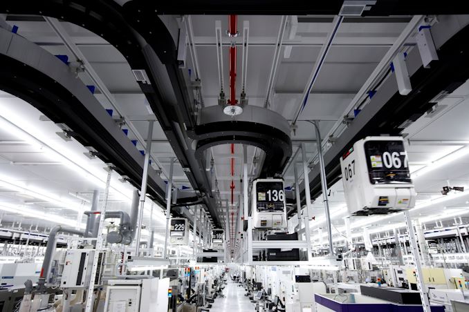
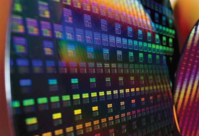
The annual IEEE International Solid-State Circuits Conference covers a range of topics of interest to AnandTech. Every year the conference includes a session on non-volatile memories where most of the NAND flash memory manufacturers share technical details of their latest developments. At the conference we get more information than these companies are usually willing to share in press briefings, and the presentations are usually about technology that will be hitting the market during the coming year.


At ISSCC 2021 this week, four of the six major 3D NAND flash memory manufacturers are presenting their newest 3D NAND technology. Samsung, SK hynix and Kioxia (+Western Digital) are sharing their latest 3D TLC NAND designs and Intel is presenting their 144-layer 3D QLC NAND. Not participating this year are Micron (who announced their 176L 3D NAND late last year) and Chinese newcomer YMTC.


3D TLC (3-bit per cell) Updates


Samsung, SK hynix, and Kioxia/WD presented information about their upcoming generations of 3D TLC. Not shown here is Micron’s 176L TLC, because they haven’t released most of this data for their latest generation of 3D NAND.


3D TLC NAND Flash Memory

ISSCC Presentations
  Samsung SK hynix Kioxia (Toshiba)

WD
Year Presented at ISSCC 2021 2019 2021 2021 2019 2018
Layers   128 176 >170 128 96
Die Capacity 512 Gb 512 Gb 512 Gb 1 Tb 512 Gb 512 Gb
Die Size (mm2)   101.58   98 66 86
Density (Gbit/mm2) 8.5 5 10.8 10.4 7.8 5.95
IO Speed 2.0 Gb/s 1.2 Gb/s 1.6 Gb/s 2.0 Gb/s 1.066 Gb/s 533 Mb/s
Program Throughput 184 MB/s 82 MB/s 168 MB/s 160 MB/s 132 MB/s 57 MB/s
Read Latency (tR) 40 µs 45 µs 50 µs 50 µs 56 µs 58 µs
Erase Block Size         24 MB 18 MB
Planes 4? 2 4 4 4 2
CuA / PuC Yes No Yes Yes Yes No


Unsurprisingly, it looks likely that Samsung will again be in the lead for performance, with the lowest read latency and fastest write speeds. However, their bit density is still clearly lagging even though they’re claiming a 70% jump with this generation. In the past, their lagging density hasn’t been as much of a downside as it might appear at first glance, because Samsung has been able to avoid using string stacking and can manufacture a stack of 128 layers as a single deck while their competitors have all had to split their stack into two decks, increasing the number of fab steps required. This might be the generation that brings Samsung’s inevitable adoption of string stacking, but if that’s the case then their lingering density disadvantage is rather disappointing. On the other hand, if they’ve managed to put off that transition for one more generation and achieved this kind of density increase only using a combination of other techniques (most notably a CMOS under Array layout), then it’s a very impressive advance and it would be safe to say that Samsung is years ahead of the competition when it comes to the high aspect ratio etching of the vertical channels that is the most critical fab step in scaling 3D NAND. We’ll know more once Samsung discloses the actual layer count, but they’re keeping that secret for now—which hints that they don’t expect to have the highest layer count to brag about.


The TLC parts described by SK hynix and Kioxia/WD look fairly similar, save for the big difference that SK hynix is talking about a 512Gb die and Kioxia is talking about a 1Tb die. Both designs look to have similar performance and density, though Kioxia is touting a higher NAND interface speed. Kioxia and Western Digital have put out a press release announcing 162-layer 3D NAND, so they’re a bit behind SK hynix and Micron for total layer count. That press release also mentions a 10% improvement in the horizontal density of their cell array, so Kioxia and Western Digital are probably packing the vertical channels closer together than any of their competitors.


3D QLC (4-bit per cell) Updates


The only company with updates this year on QLC is Intel.


3D QLC NAND Flash Memory

ISSCC Presentations
  Intel Samsung SK hynix Kioxia

WD
Year Presented at ISSCC 2021 2020 2020 2018 2020 2019
Layers 144 96 92 64 96 96
Die Capacity 1 Tb 1 Tb 1 Tb 1 Tb 1 Tb 1.33 Tb
Die Size (mm2) 74.0 114.6 136 182 122 158.4
Density (Gbit/mm2) 13.8 8.9 7.53 5.63 8.4 8.5
IO Speed 1.2 Gb/s 800 Mb/s 1.2 Gb/s 1.0 Gb/s 800 Mb/s 800 Mb/s
Program Throughput 40 MB/s 31.5 MB/s 18 MB/s 12 MB/s 30 MB/s 9.3 MB/s
Program Latency (tPROG) 1630 µs 2080 µs 2 ms 3 ms 2.15 ms 3380 µs
Read Latency

(tR)
Avg 85 µs 90 µs 110 µs 145 µs 170 µs 160 µs
Max 128 µs 168 µs       165 µs
Erase Block Size 48 MB 96 MB   16 MB 24 MB 24 MB
Planes 4 4 2 2 4 2


In general, Intel has been more focused on QLC NAND than any of its competitors. This 144L QLC is the first generation of 3D NAND Intel hasn’t co-developed with Micron, and it is unique in several respects. Intel is taking its 3D NAND technology in different directions from the rest of the industry will have interesting ramifications for their agreement to sell the NAND flash business to SK hynix, but in the short term it seems like Intel is getting the NAND they want to be selling. With only 144 layers, Intel is almost certainly now in the last place for total layer count. Compared to 9x-layer QLC, Intel has much better performance and density—but QLC versions of the new TLC described by SK hynix and Kioxia should have comparable density. Intel has backed off from the frankly astronomical erase block size their 96L QLC used, but the 48MB block size of their new 144L QLC still seems a bit high.


CMOS Under Array From Everyone


Intel and Micron’s now-dissolved joint venture was the second NAND flash manufacturer to make the switch to 3D NAND, after Samsung. The most significant innovation the Intel/Micron 3D NAND brought to the industry was the CMOS Under the Array (CuA) design. This places most of the NAND die’s peripheral circuitry—page buffers, sense amplifiers, charge pumps, etc.—under the vertical stack of memory cells instead of alongside.


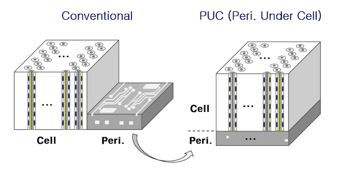
This change saves a big chunk of die space and allows for over 90% of the die area to be used for the memory cell array. SK hynix was next to make this switch, which they call “Periphery under Cell” (PuC). The rest of the manufacturers are now also onboard: Kioxia (then Toshiba) and Western Digital presented a 128-layer CuA design at ISSCC 2019 but their fifth generation BiCS 3D NAND ended up going into production as a 112L design without CuA. Their ISSCC presentation this year is for a “170+” layer design with CuA, and they’ve put out a press release confirming that their sixth generation BiCS 3D NAND will be a 162-layer design with CuA.


Aside from saving die space, a CuA/PuC style design for 3D NAND allows for a die to include more peripheral circuitry than would otherwise be cost-effective. This makes it practical to divide a die’s memory array into more separate planes, each with their own copies of much of the peripheral circuitry. Most 3D NAND that has been built without a CuA layout has used just two planes per die, but now that everyone is using CuA the standard is four planes per die. This provides extra parallelism that increases the performance per die and offsets the overall SSD performance drop that usually comes from using fewer dies to reach the same total capacity.


A CuA structure is not without its challenges and downsides. When a manufacturer first switches to CuA they get a big increase in available die space for peripheral circuitry. But after that, each successive generation that adds layers means there’s less die space available for managing the same number of memory cells, so peripheral circuitry still has to shrink. Putting peripheral circuitry under the memory cell array also introduces new constraints. For example, Samsung’s ISSCC presentation this year mentions the challenges of constructing large capacitors for the charge pumps when they can no longer use the tall metal structures that are simple to include alongside the 3D NAND stack.


Better On-Die Parallelism: Four Planes Per Die


Dividing a NAND flash die into four planes allows for the die to handle more operations in parallel, but doesn’t make it behave quite like four independent dies. There are restrictions on what can be done in parallel: for example, simultaneous writes still have to go to the same word line within each plane. But as the number of planes in a flash die grows, manufacturers have been working to loosen some of those restrictions. In previous years, manufacturers have introduced *independent* multi-plane reads, meaning simultaneous reads in different planes don’t have any restrictions on the locations within each plane that are being read—a big win for random read throughput.


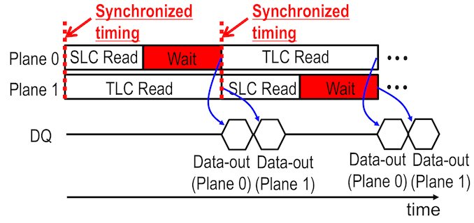
Now, another restriction on multi-plane operations is being relaxed: the timing of read operations in different planes doesn’t need to line up. This makes it possible for one plane to perform multiple reads from SLC pages while another plane is performing a single slower read from TLC or QLC pages. This capability is called Asynchronous Independent (Multi-)Plane Read. The practical effect is that for read operations, a large 4-plane die can now match the performance of four smaller 1-plane dies. This mitigates many of the performance downsides that higher per-die capacity brings to SSDs that only have one or two dies per channel.


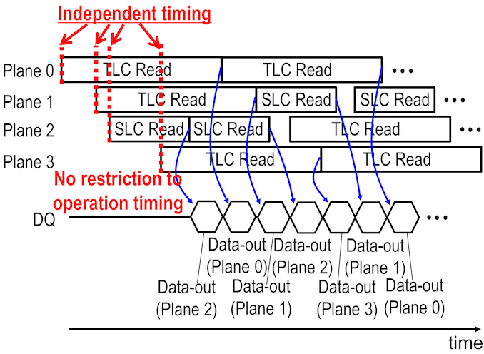
Kioxia and WD reported that implementing this capability required them to stop sharing charge pumps between planes, in order to avoid poorly-timed voltage and current fluctuations that would have resulted from unsynchronized read operations. Intel is also halfway to this capability with their 4-plane 144L QLC: planes are paired up into plane groups, and each plane group can perform reads without needing to align with the timing of reads in the other plane group.


NAND IO Speeds Outpacing SSD Controller Support


The new TLC NAND parts described at ISSCC support IO speeds ranging from 1.6 to 2.0 Gb/s for communication between the NAND flash dies and the SSD controller. The fastest NAND in SSDs currently on the market runs at 1.2-1.4Gb/s. The NAND manufacturers can benefit from vertical integration by ensuring that their own SSD controller designs used for their own SSDs will be ready to support these higher IO speeds, but other SSD vendors that rely on third-party controllers may be left behind. Phison’s latest E18 8-channel controller for high-end PCIe 4.0 SSDs only supports 1.2Gb/s IO speeds, and their upcoming E21T 4-channel NVMe controller supports 1.6Gb/s. Silicon Motion’s 8-channel SM2264 and 4-channel SM2267 support 1.6Gb/s and 1.2Gb/s IO speeds respectively.


Since 8 channels running at 1.2Gb/s is already enough for a SSD to saturate a PCIe 4.0 x4 connection, these new higher IO speeds will not be of much use to high-end SSDs until PCIe 5.0 arrives. But more affordable 4-channel consumer SSD controllers will be able to use these higher speeds to move up well into PCIe 4.0 performance territory, matching or exceeding the throughput that the first PCIe 4.0 SSD controller (Phison E16, 8ch @ 800Mb/s) offered. As demonstrated by drives like the SK hynix Gold P31, an advanced 4-channel controller supporting high IO speeds on each channel can be very competitive on performance while operating with far higher power efficiency than 8-channel controllers.


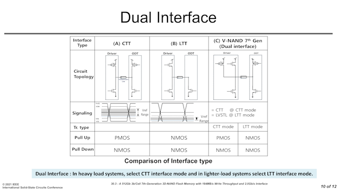
Hitting these higher IO speeds requires major upgrades to the interface logic on the NAND dies, and as we’ve seen with other high-speed interfaces like PCI Express, increasing power consumption is a major concern. Samsung is addressing this by using dual-mode drivers and termination. When higher drive strength is needed because of more load on the bus (from more dies per channel), the’ll use a PMOS transistor for pull-up, and otherwise they can use a NMOS transistor and cut the power consumption of the driver by more than half. This gives Samsung a single interface design that will work well for both small consumer SSDs and large enterprise drives with many more dies per channel. (In the past Samsung has added separate retimer dies to multi-chip packages that stack lots of NAND dies together on the same one or two channels. We’re not sure if Samsung is still using this technique.)


String Stacking: First Triple-Deck NAND


String stacking has been viewed as something of a necessary evil for scaling up 3D NAND to higher layer counts. Only Samsung has managed to build more than 100 layers of 3D NAND at a time, and everyone else has long since switched to stacking two decks each with a more reasonable layer count. This means that eg. Micron’s 176-layer 3D NAND is built as 88 layers of memory cells, then another 88 layers are constructed on top. This drives up cost compared to doing all the layers at once, and it requires careful alignment at the interface between decks. But the alternative would be to make the vertical channels much wider, so that the aspect ratio (width vs depth) would stay within the realm of what can be feasibly etched by current fab techniques.


Intel’s 144L QLC design includes the surprise that they are already moving to a 3-deck stack: 48+48+48 layers rather than the 72+72 we would expect. Since their previous generation is a 48+48 layer (96L total) design, it’s possible that they have changed very little about how the memory array itself is fabricated aside from repeating the same sequence of deposition, etch and fill steps a third time. Intel is taking a hit on fab throughput with this approach, but it probably helps them better control the variation in channel and cell dimensions from the top to bottom of the stack, which may be more of a concern given their focus on QLC and their unique decision to still use a floating gate memory cell rather than switching to a charge trap cell like everyone else.


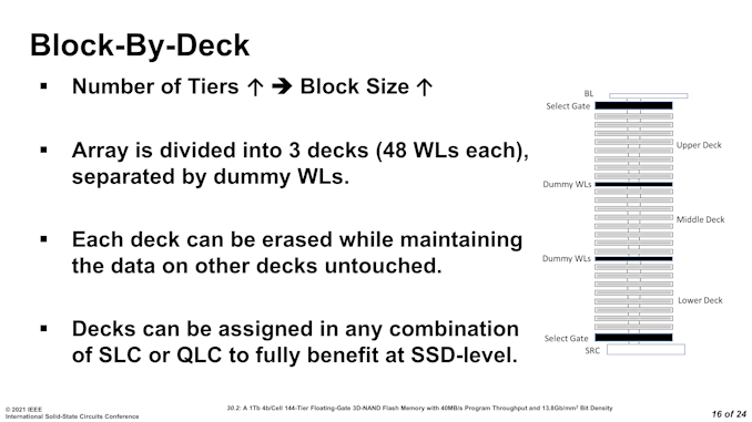
To go along with this triple-deck structure, Intel has reorganized how they handle erase blocks, and now each of the three decks constitutes a separate collection of erase blocks. That means the middle third of a 144L string can now be erased without interfering with the data stored in the other two thirds of the string. Dividing blocks by decks is also how Intel was able to reduce the 96 MB block size with their 96L QLC down to a less extreme 48MB block size.


A Small Caveat about Academic Conferences


It’s important to understand that ISSCC, where these updates are presented, is an academic conference. The presentations are not product announcements and the papers are not product spec sheets. The designs presented at ISSCC don’t always match what goes into mass production. For example, Kioxia/WD in the past have presented designs for 128L and “170+” layer NAND, but their actual fifth and sixth generation BiCS NAND as mass produced are 112L and 162L designs. They also, despite mentioning it in their 2019 talk, deferred a switch to a more dense ‘CMOS under Array (CuA) structure’ to a later product line.  Specifications such as write performance are also often presented as best-case, and real world products end up being a notch below what is presented.


Despite the coming together of all these companies under one conference, even when the presentation does match the eventual product, what we learn from ISSCC is usually imperfect and incomplete information. The companies are inconsistent about what metrics they report, and we usually get information for only one die design per generation—a company might present their 512Gbit design even if they’re planning to manufacture both 512Gbit and 256Gbit parts. In recent years several companies seem to be alternating between talking about their QLC one year and TLC the next. In spite of all of that, ISSCC presentations on 3D NAND are still a great way to gauge how the state of the art has progressed and where the industry as a whole is headed.


About half the content of these presentations is clever schemes for micromanaging voltages applied to various wires to optimize the read, program and erase processes. There are complex tradeoffs between speed, accuracy, wear and other factors. we’re not going to dig into all of these details, other than to say that programming a cell to the desired voltage (and without disturbing other cells) is not a simple process, and even reading from a TLC or QLC cell is quite a bit more complicated than reading from a DRAM or SRAM cell. We’re more interested in any major structural changes in the dies themselves, and the end results of all the finessing of voltages: the speeds at which a page of memory can be read or programmed.


Source Material: 68th ISSCC, Feb 13-22nd 2021


Source: AnandTech – 2021 NAND Flash Updates from ISSCC: The Leaning Towers of TLC and QLC

Toshiba Unveils World's First FC-MAMR HDD: 18 TB, Helium Filled

Toshiba this week announced the industry’s first hard drive featuring flux-control microwave-assisted magnetic recording (FC-MAMR) technology. The new MG09-series HDDs are designed primarily for nearline and enterprise applications, they offer an 18 TB capacity along with an ultra-low idle power consumption. 


The Toshiba MG09-series 3.5-inch 18 TB HDD are based on the company’s 3rd generation nine-platter helium sealed platform that features 18 heads with a microwave-emitting component which changes magnetic coercivity of the platters before writing data. The HD disks are made by Showa Denko K.K. (SDK), a long-time partner of Toshiba. Each aluminum platter is about 0.635 mm thick, it features an areal density of around 1.5 Tb/inch2 and can store up to 2 TB of data. The MG09 family also includes a 16 TB model which presumably features a lower number of platters (based on the same performance rating).


For modern enterprise and nearline 3.5-inch HDDs, Toshiba’s MG09-series drives uses a motor with a 7200-RPM spindle speed. The HDDs are also equipped with a 512 MB buffer and are rated for a 281 MB/s maximum sustained data transfer rate. Unfortunately, Toshiba has not updated the random access performance of the new products, though it is likely that their per-TB IOPS performance is lower when compared to predecessors. The manufacturer will offer its new drives both with SATA 3.3 (6 Gbps) and SAS 3.0 (12 Gbps) interfaces as well as a selection of logical data block length.


One of the noteworthy things about Toshiba’s MG09-series FC-MAMR HDDs is their power consumption. In active idle mode, they typically consume 4.16/4.54 Watts (SATA/SAS models), which is considerably lower when compared with Seagate’s Exos X18 as well as Western Digital’s Ultrastar DC HC550. As far as power consumption efficiency at idle (large hard drives could spend plenty of time idling) is concerned, the 18 TB MG09 is an undeniable champion consuming just 0.23 Watts per TB (in case of the SATA version). Meanwhile, the new drives are rated for 8.35/8.74 Watts (SATA/SAS SKUs) during read/write operations, which is higher when compared to the DC HC550 as well as predecessors from the MG07 and the MG08-series.


Brief Specifications of Toshiba’s MG09 HDDs
Capacity 18 TB 16 TB
Platters 9 8
Heads 18 16
Recording Technology Flux-control microwave-assisted

magnetic recording (FC-MAMR)
RPM 7200 RPM
Interface SATA 6 Gbps/SAS 12 Gbps
DRAM Cache 512 MB
Persistent Write Cache Yes
Helium-Filling Yes
Sequential Data Transfer Rate (host to/from drive) 281 MB/s
MTBF 2.5 million
Rated Annual Workload 550 TB
Acoustics (idle) 20 dB
Power Consumption Random read/write SATA: 8.35 W

SAS: 8.74 W
Idle SATA: 4.16 W

SAS: 4.54 W
Warranty 5 Years


As the MG09 family of hard drives are intended for datacenter racks that accommodate hundreds of vibrating HDDs, they feature numerous enhancements to ensure consistent performance, reliability, and durability. Typically such enhancements include top and bottom attached motors, RVFF, as well as environmental sensors. Like all modern drives for 24/7 applications, Toshiba’s MG09-series units are rated for a 550 TB average annualized workload, 2.5 million hours MTBF, and are covered with a standard five-year warranty.


Also, the new MG09 hard drives support Toshiba’s persistent write cache (PWC) with power loss protection (PLP) technology, which is crucial for 4K sector drives that emulate 512B sectors. The PWC with PLP feature guards data in case of power loss while performing read-modify-write (RMW) operation to align the source write request with the physical sectors it has to modify. This capability allows the company to address its clients who run legacy systems that still require high capacities. Also, the new MG09 family includes Sanitize Instant Erase (SIE) and Self Encrypting Drive (SED) models.


Toshiba has been working on its MG09-series FC-MAMR HDDs for at least two years already. Last year the company said it had made ‘significant investments in manufacturing facilities’ and promised to start shipments of its 18 TB hard drives by March 31, 2021. This week the company reaffirmed its plan and said it would begin sample shipments of its 18 TB MG09-series MAMR HDDs ‘at the end of March 2021.’


Source: Toshiba


Source: AnandTech – Toshiba Unveils World’s First FC-MAMR HDD: 18 TB, Helium Filled