Microsoft Springs A Surface Launch: Surface Laptop 4 Announced With Custom Ryzen

Microsoft tends to update their Surface lineup on an irregular schedule, not necessarily following the updated CPUs that are generally announced on a mostly annual cadence. Today Microsoft is announcing an updated Surface Laptop, dubbed the Surface Laptop 4, and brings the hardware up to date, somewhat at least. Also, with the explosion in video conferencing as a result of the Covid-19 global pandemic, the company is also announcing a slew of accessories to improve the Microsoft Teams experience.


Surface Laptop 4: Intel Tiger Lake and Custom AMD Processors


Microsoft’s update schedule often means their products linger in the market with specifications that are no longer current. Perhaps no product has felt that more than the Microsoft Surface Laptop 3, especially the AMD version, which launched in late 2019. Based on AMD’s Picasso platform at the time, the AMD Ryzen Surface Edition processor suffered from poor battery life – an issue which AMD resolved with the launch of their Ryzen 4000 series “Renoir” processors just a few months later.


Today, Microsoft is rectifying this, but not going quite as far as you would expect for a device launching in April 2021. Once again, Microsoft will be launching both Intel and AMD powered versions of the Surface Laptop 4, and again, the AMD models will feature a custom Ryzen processor. However, despite AMD releasing their Ryzen 5000 series “Cezanne” lineup, the Surface Laptop 4 will feature the older Renoir platform. As disappointing as this is, Renoir was a very capable platform, with great performance, and great battery life. Perhaps the Surface Laptop 4 refresh was supposed to come in late 2020, but was delayed by Covid, but regardless, even with the Ryzen 4000 series powering it, the Surface Laptop 4 should be a big improvement over the Surface Laptop 3.


Microsoft Surface Laptop 4
  13.5-Inch 15-Inch
Processor Intel Core i5-1035G7


Intel Core i5-1145G7


Intel Core i7-1185G7


AMD Ryzen 5 4680U


AMD Ryzen 7 4980U
Intel Core i7-1185G7


AMD Ryzen 7 4980U
Memory 8GB/16GB/32GB LPDDR4X-3733MHz Intel: 8GB/16GB/32GB LPDDR4X-3733MHz

AMD: 8GB/16GB/32GB DDR4-2400MHz
Graphics Intel: Intel Iris Xe Grahics

AMD: AMD Ryzen Microsoft Surface Edition Radeon Graphics
Display 13.5″ 2256×1504 3:2 PixelSense

Touch and Pen support

Individually calibrated panels
15″ 2496×1664 3:2 PixelSense

Touch and Pen support

Individually calibrated panels
Storage 256 GB, 512 GB PCIe NVMe

Removable Drive
Networking Wi-Fi 6 802.11ax

Bluetooth 5.0
Audio Omnisonic Speakers

Dolby Audio 9
Battery Up to 19 hours on AMD Ryzen 5

Up to 17 hours on Intel Core i5
Up to 17.5 hours on AMD Ryzen 5

Up to 16.5 hours on Intel Core i5
Right Side Surface Connect Port
Left Side USB Type-A

USB Type-C

Headset Jack
Dimensions 308 x 223 x 14.51 mm (12.1 x 8.8 x 0.57 inches) 339.5 x 244 x 14.69 mm (13.4 x 9.6 x 0.57 inches)
Weight Fabric: 1.26kg

Metal: 1.29kg
1.54kg
Camera Front: 720p Camera and Windows Hello support

Dual far-field Studio Mics
Extras Surface Pen and Dial (sold separately)

TPM 2.0
Pricing Starting at $999 USD Starting at $1099 USD


Perhaps disappointingly for AMD fans, customers who opt for the Intel-based Surface Laptop 4 will not have to suffer such indignities. Surface Laptop 4 will ship with the latest Intel Tiger Lake platform, which brings slightly updated CPU cores, and much more powerful Intel Xe graphics, on Intel’s 10 nm process.


Also good news is that Microsoft has drastically expanded the lineup in terms of choice, with both the 13.5-inch, and the 15-inch models both available with AMD or Intel options, whereas the AMD version was only available in the 15-inch for Surface Laptop 3, and the Intel Ice Lake was only available as the “Business” edition. For the Surface Laptop 4, there is plenty of choice.


Additional choices are now available in terms of color too, with Microsoft adding an Ice Blue option to the existing Platinum, Matte Black, and Sandstone options. One of the most unique aspects of the original Surface Laptop was the Alcantara keyboard deck, and Microsoft has kept that as an option for the 13.5-inch model in either Platinum or Ice Blue.


Microsoft is claiming up to 19 hours of battery life on the Surface Laptop 4, in 13.5-inch guise and with the AMD Ryzen processor. This is a significant upgrade over the outgoing model, and comes alongside much better performance. Memory is 8 GB to 32 GB, and storage is 256 GB to 1 TB. Microsoft used to be guilty of offering specifications that were too low for even a base model, but 8 GB / 256 GB is a reasonable low-end configuration.


Microsoft pushed back on USB Type-C, and the company still is pushing back on Thunderbolt, even on the Intel-based devices. Thunderbolt 4 brings a lot of standardization, and would have been nice to see, but sadly, the company refuses to support it. One area where they can be commended though is that they are expanding their removable SSD support to the Surface Laptop 4, allowing easier expandability in the future. The drives are, as far as we can tell, still PCIe 3.0 NVMe drives, even though the Intel Tiger Lake model would support PCIe 4.0 storage. We’ll try to get clarification on if the slot supports it or not though.


The Surface Laptop has always offered great build quality, along with the fantastic PixelSense display in the now ubiquitous Surface 3:2 aspect ratio. While there are no major changes to the chassis, the updated internals, coupled with the light weight and good display, bring the Surface Laptop back into the equation.


The Surface Laptop 4 is available for pre-order, starting at $999 for the 13.5-inch, and $1099 for the 15-inch models.


Source: Microsoft


Source: AnandTech – Microsoft Springs A Surface Launch: Surface Laptop 4 Announced With Custom Ryzen

NVIDIA Unveils Grace: A High-Performance Arm Server CPU For Use In Big AI Systems

Kicking off another busy Spring GPU Technology Conference for NVIDIA, this morning the graphics and accelerator designer is announcing that they are going to once again design their own Arm-based CPU. Dubbed Grace – after Grace Hopper, the computer programming pioneer and US Navy rear admiral – the CPU is NVIDIA’s latest stab at more fully vertically integrating their hardware stack by being able to offer a high-performance CPU alongside their regular GPU wares. According to NVIDIA, the chip is being designed specifically for large-scale neural network workloads, and is expected to become available in NVIDIA products in 2023.


Source: AnandTech – NVIDIA Unveils Grace: A High-Performance Arm Server CPU For Use In Big AI Systems

The NVIDIA GTC 2021 Keynote Live Blog (Starts at 8:30am PT/16:30 UTC)

Join us at 8:30am PT for our coverage of NVIDIA’s annual GPU Technology Conference keynote address. The traditional kick-off to the show – be it physical or virtual – NVIDIA’s annual spring keynote is showcase for NVIDIA’s vision for the next 12 to 24 months across all of their segments, from graphics to AI to automotive. Along with slew of product announcements, the presentation, delivered by CEO (and lovely kitchen owner) Jensen Huang always contains a few surprises.


Due to the coronavirus, this year’s show is once again virtual. However, with a full year to prepare for it, NVIDIA is delivering a much more traditional event. This includes the keynote itself, which although pre-recorded, is being broadcast as one continuous presentation rather than uploaded and unlocked as multiple segments all at once. Big topics of conversation this year will include graphics, networking, automotive, and AI, especially as NVIDIA’s now a year into shipping its flagship A100 accelerator. And though A100 isn’t due for a replacement this year, we may get some insight into how NVIDIA intends to continue to fend off AMD and Intel, both of whom have server GPU and AI plans that are finally starting to come together.


Source: AnandTech – The NVIDIA GTC 2021 Keynote Live Blog (Starts at 8:30am PT/16:30 UTC)

AMD Issues Updated Speculative Spectre Security Status: Predictive Store Forwarding

The mention of Spectre and Meltdown is enough to send chills down any InfoSec spine. A number of these batches of security vulnerabilities deal with speculative execution, and how a processor might leak data while executing code in a speculative manner. This week AMD has pre-empted the security space by detailing a potential security concerns regarding its new Zen 3-based Predictive Store Forwarding feature designed to improve code performance by predicting dependencies between loads and stores. AMD is clear to point out that most users will not need to take any action, as the risk for general consumer use to any breach is low, and no known code is vulnerable.


Source: AnandTech – AMD Issues Updated Speculative Spectre Security Status: Predictive Store Forwarding

Silicon Motion Announces SM2708 SD Express Controller

Silicon Motion has announced their first SD Card controller to support the NVMe-based SD Express interface. The new SM2708 controller is capable of sequential transfer speeds of 1700 MB/s, vastly higher than the 104 MB/s most SD devices and cards are limited to using the older but widely-supported UHS-I interface.


In 2018, version 7.0 of the SD specification introduced the PCIe and NVMe-based SD Express interface as the new way forward for SD cards. The older UHS-II and UHS-III interfaces developed in versions 4 through 6 of the SD standard and capable of speeds from 156 MB/s to 624 MB/s were abandoned in favor of a single lane of PCIe gen3 (~985 MB/s). Last year, version 8.0 of the SD specification added support for PCIe gen4 speeds and a second PCIe lane, bringing the theoretical maximum transfer speed up to almost 4 GB/s.


Silicon Motion’s SM2708 is a two-lane controller, but still using PCIe gen3 speed, hence the top speed can’t quite reach 2 GB/s. This has the potential to bring SD card performance up to near the levels of entry-level consumer NVMe SSDs for laptops and desktops—competitive with SSDs based on slightly-outdated controllers like the Phison E8T or Silicon Motion SM2263XT. The SM2708 controller uses two NAND channels instead of the four typically used by entry-level SSD controllers, but the SM2708 is capable of a 1200 MT/s IO speed that allows it to get good performance out of recent NAND flash generations without the power and size penalties of a four-channel solution.


In 2019, Silicon Motion’s primary competitor Phison announced their PS5017 SD Express controller. This is based on the earlier SD 7.0 specification and thus is a PCIe 3 x1 design and limited to about 870 MB/s. In February 2021 Phison announced they were about to start shipping cards based on this solution. Silicon Motion’s SM2708 controller might not take that long to turn into actual products, but they clearly have missed out on the first round of SD Express competition—though they may be able to leapfrog Phison’s solution.


Underlying all the developments related to recent flash memory card standards has been the challenge of poor adoption. For years, storage tech has been advancing much faster than camera tech. Storage technology companies stand ready to supply more advanced memory cards, but they cannot succeed in the market unless there are host devices ready to use the higher performance. We’ve seen a decade of failed successors to the old SD and CF standards that now seem pitifully slow. SD’s UHS-II and UHS-III, CF’s CFast and XQD, and UFS cards have all been demonstrated as working technologies and all eventually made it to market to some extent, but with very limited success. The SD and CF worlds have converged on PCIe and NVMe as the way forward, adopting interfaces that already have a thriving ecosystem and long-term viability in other form factors. That makes it more likely that standards like SD Express will actually catch on, but it may still be several years before PCIe-based interfaces are supported on any phones or more than a handful of high-end cameras.


Source: AnandTech – Silicon Motion Announces SM2708 SD Express Controller

GIGABYTE Server: Three New E-ATX Motherboards For Intel Ice Lake-SP Xeons

Hot on the heels of Intel’s latest Ice Lake-SP 3rd Generation Xeon Scalable processor launch, GIGABYTE Server has listed three new motherboards designed for server use. The GIGABYTE Server MU92-TU1, the MU92-TU0, and MU72-SU0 all offer different levels of features and controllers and are based on Intel’s C621A chipset for 3rd Gen Xeon Scalable. Two are built on the E-ATX form factor, with one ATX model, with features varying between sixteen memory slots, different dual Ethernet configurations, and all come with an integrated ASPEED BMC controller.


The Intel Xeon Scalable processor stack is designed for use in servers, with some likely professional applications alongside the usual Cloud and Datacenter operations. With some new refinements of its 10 nm process for Enterprise situations, including the use of SGX and a focus for customized crypto acceleration. There are many Intel Xeon Scalable Ice Lake-SP SKUs in the product stack, including the top tier 40-core Xeon Platinum 8380 model the way down to the entry-level Xeon Silver 4309 model. 


Read our Intel 3rd Gen Xeon Scalable Review below:


To complement the 3rd Generation Intel Xeon Scalable for Enterprise launch, GIGABYTE has readied up three new motherboards. Based on the Intel C621A chipset and all using one LGA4189 socket, GIGABYTE Server MU92-TU0, the MU92-TU1, and MU72-SU0 include some interesting and notable features.


MU92-TU0 and MU92-TU1


Starting with the E-ATX sized pairing, the MU92-TU0 and MU92-TU1 both include seven full-length PCIe 4.0 slots, which can operate at x16/x0/x16/x0/x16/x0/x16, or x16/x8/x8/x8/x8/x8/x8, with sixteen memory slots that can support up to 2 TB of 3DS RDIMM/LRDIMM DDR4-3200 memory, with regular LRDIMMs of up to 128 GB and RDIMM memory up to 64 GB also supported. For storage, both the MU92-TU0 and MU92-TU1 include a single PCIe 3.0 x4 M.2 slot, with two SATA ports and two SlimSAS ports with support for up to eight SATA ports. Both models also include a standard 24-pin ATX 12 V motherboard power input, two 8-pin 12 ATX CPU power inputs, seven 4-pin fan headers, an Intel VROC connector, a PMBus, and an IPMB connector.


GIGABYTE Server MU92-TU0 motherboard (E-ATX)


Aesthetically the same with GIGABYTE’s blue PCB, the only difference between the MU92-TU0 and MU92-TU1 is the MU92-TU1 is using ASPEED’s latest ARM-based AST2600 BMC controller. The slightly lesser spec MU92-TU0 uses an ASPEED AST2500 BMC controller, while both models include dual 10 GBase-T Ethernet, which is powered by an Intel X710-AT2 controller. Also present on both models are two USB 3.0 Type-A ports, a D-Sub video output and MLAN port for the BMC, a COM port, and an ID button with LED. 


MU72-SU0


The GIGABYTE Server MU72-SU0 is using an ATX form factor featuring a single LGA4189 socket. It includes eight memory slots, with support for up to 2 TB of 3DS RDIMM/LRDIMM DDR4-3200 memory, and regular LRDIMMs of 128 GB and RDIMMs up to 64 GB for servers that require less memory capacity. There’s a total of seven full-length PCIe 4.0 slots, with supported configurations including both x16/x0/x16/x0/x16/x0/x16 and x16/x8/x8/x8/x8/x8/x8, with storage options including one PCIe 3.0 x4 M.2 slot, and three SlimSAS connectors which allow for up to twelve SATA ports.


GIGABYTE Server MU72-SU0 motherboard (ATX)


The MU72-SU0 uses an ASPEED AST2600 BMC controller, with a dedicated management Ethernet port and D-Sub video output, with dual Gigabit Ethernet, which is driven by a pair of Intel I210-AT Gigabit controllers. The rear panel also includes four USB 3.0 Type-A ports, a COM port, and an ID button with LED. Other avenues of connectivity around the board include seven 4-pin fan headers, a TPM header, and an Intel VROC connector. Providing power to the board is one 24-pin 12 V ATX motherboard power, one 8-pin 12 V ATX CPU power, and a 6-pin PCIe power input designed to deliver more power to the full-length PCIe slots. 


It is unknown when the GIGABYTE Server MU92-TU1, MU92-TU0, and MU72-SU0 are likely to hit retail shelves at the time of writing, but given the Ice Lake-SP processors are now released, we don’t expect it will be too long. We also don’t currently have any pricing information.


Source: GIGABYTE Server


Related Reading


Source: AnandTech – GIGABYTE Server: Three New E-ATX Motherboards For Intel Ice Lake-SP Xeons

Intel 3rd Gen Xeon Scalable (Ice Lake SP) Review: Generationally Big, Competitively Small

The launch of Intel’s Ice Lake Xeon Scalable processors has been in the wings for a number of years. The delays to Intel’s 10nm manufacturing process have given a number of setbacks to all of Intel’s proposed 10nm product lines, especially the high performance Xeon family: trying to craft 660 mm2 of silicon on a process is difficult at the best of times. But Intel has 10nm in a place where it is economically viable to start retailing large Xeon processors, and the official launch today of Intel’s 3rd Generation Xeon Scalable is on the back of over 200,000+ units shipped to major customers to date. The new flagship, the Xeon Platinum 8380, has 40 cores, offers PCIe 4.0, and takes advantage of the IPC gain in Intel’s Sunny Cove processor core. We’re testing it against the best in the market.


Source: AnandTech – Intel 3rd Gen Xeon Scalable (Ice Lake SP) Review: Generationally Big, Competitively Small

G.Skill Announces DDR4-5333 Memory Kits for Intel Rocket Lake

Designed with a focus on Intel’s latest 11th generation Rocket Lake processors and the new memory controller ratios, G.Skill has announced a wave of new memory kits designed to squeeze as much performance out of the platform. The new memory kits for Z590 and Rocket Lake feature speeds of up to DDR4-5333. They will be made available across multiple lines of its range, including the premium Trident Z Royal, Trident Z RGB, and the more affordable Ripjaw V series.


With memory performance and control getting some extra features with Intel’s 11th gen desktop, the Z590 chipset with Rocket Lake processors now supports geared memory ratios between the memory controller and the DRAM data rates. The ability of Intel’s memory controller in a 1:1 gear ratio can vary, certainly under ambient cooling methods, and not all of Intel’s silicon can handle such high frequencies. This is where the gear ratio option becomes beneficial, taking some of the strain off the memory controller and allowing for high frequencies, with G.Skill capitalizing on this with its new memory kits up to DDR4-5333.


G.Skill’s Trident Z Royal DDR4 Memory in Gold


The new G.Skill memory kits designed for Intel’s Z590 (with Rocket Lake) start from DDR4-4266 with CL19 ratings, with two available capacities: dual-channel 32 GB (2×16) and 64 GB (2×32) kits. Also set to be available include DDR4-4400 kits with CL17 and CL18 latencies, including an operating voltage of 1.50 V in both the 32 GB and 16 GB kits.


Moving up, there’s one kit of DDR4-4600 with CL20 with a total capacity of 64 GB (2 x 32 GB) and three different flavors of DDR4-4800; CL17 and CL18 with 2 x 8 GB kits, and CL20 with 2 x 16 GB. There’s one 32 GB (2 x 16 GB) kit at DDR4-5066 with CL19 and an operating voltage of 1.6 V, with one kit maxing out at DDR4-5333 and CL21 latencies, with 2 x 8 GB memory sticks.


G.Skill Memory For Intel Z590 (Rocket Lake)
Rating (MT/s) Latency Voltage Capacity
DDR4-4266 19-26-26-46

19-26-26-46
1.45 V

1.50 V
32 GB (2 x 16 GB)

64 GB (2 x 32 GB)
DDR4-4400 17-18-18-38

18-24-24-44
1.50 V

1.50 V
32 GB (2 x 16 GB)

16 GB (2 x 8 GB)
DDR4-4600 20-30-30-50 1.50 V 64 GB (2 x 32 GB)
DDR4-4800 17-19-19-39

19-28-28-48

20-30-30-50
1.60 V

1.50 V

1.55 V
16 GB (2 x 8 GB)

16 GB (2 x 8 GB)

32 GB (2 x 16 GB)
DDR4-5066 20-30-30-50 1.60 V 32 GB (2 x 16 GB)

16 GB (2 x 8 GB)
DDR4-5333 22-32-32-52 1.60 V 16 GB (2 x 8 GB)


G.Skill has announced that its new Rocket Lake and Z590 kits have been validated on the ASUS ROG Strix Z590-E Gaming WIFI, the ASUS ROG Maximus XIII Apex, and MSI’s MEG Z590I Unify motherboards with an Intel Core i9-11900K processor. G.Skill also stated that its DDR4-4800 CL17 16 GB (2 x 8 GB) kit uses Samsung B-die memory chips but didn’t specify if this was the case across its range.


At the time of writing, G.Skill hasn’t given us any pricing, but they are expected to launch in Q2 2021. With memory prices set to rise throughout the year, these kits aren’t likely to be cheap. The G.Skill Trident Z Royal and Trident Z RGB will likely feature at the higher end of the pricing spectrum, with its Ripjaw Z series sitting as its entry point.


Related Reading


Source: AnandTech – G.Skill Announces DDR4-5333 Memory Kits for Intel Rocket Lake

LG Calls it Quits, To Close Mobile Phone Business

This morning, LG issued a press release that announced the board of directors had decided to close down the conglomerate’s mobile phone business. The news is unfortunate, however isn’t too surprising given the mobile division had been accruing continuous operational losses over the last 6 years, greatly denting the company’s financials.


SEOUL, April 5, 2021 — LG Electronics Inc. (LG) announced that it is closing its mobile business unit. The decision was approved by its board of directors earlier today.


LG’s strategic decision to exit the incredibly competitive mobile phone sector will enable the company to focus resources in growth areas such as electric vehicle components, connected devices, smart homes, robotics, artificial intelligence and business-to-business solutions, as well as platforms and services.


LG will provide service support and software updates for customers of existing mobile products for a period of time which will vary by region. LG will work collaboratively with suppliers and business partners throughout the closure of the mobile phone business. Details related to employment will be determined at the local level.


Moving forward, LG will continue to leverage its mobile expertise and develop mobility-related technologies such as 6G to help further strengthen competitiveness in other business areas. Core technologies developed during the two decades of LG’s mobile business operations will also be retained and applied to existing and future products.


LG had been one of the major mobile pioneers in the feature phone market, and also a larger player in the early 2010’s with many notable earlier successes such as the LG G2 or the G3.


Unfortunately in the following years, the company had been struck hard by chains of hardware disadvantages, ranging from the Snapdragon 810/808 generation in the G4, a failed attempt at hardware modularity in the G5. LG had also suffered issues over several generations in their OLED display attempts, plagued by lower quality panels with image quality issues, or power efficiency deficits compared to other alternatives in the market who used Samsung Display OLED panels.


At one point, LG had plans to deploy their own in-house design “Nuclun” SoCs into their mobile devices, announcing their partnership with Intel Custom Foundry to produce a leading-edge design on Intel’s 10nm process node. Unfortunately, the project burned to the ground along with Intel’s 10nm struggles, with the chips never seeing the light of day.


LG’s latest device attempts in the form of the V60 and the VELVET were actually greater leaps for the company’s designs as well as executions, however all coming too late, with a continuing problem of availability of the devices, as LG still ran with an availability model of working closely with carriers and releasing devices only in markets where carriers decided they were interested in supporting that device.


The company will be winding down its mobile business through July 31st, refocusing its resources into other divisions of the conglomerate.


Source: AnandTech – LG Calls it Quits, To Close Mobile Phone Business

SK Hynix to Build $106 Billion Fab Cluster: 800,000 Wafer Starts a Month

Capping off a busy week for fab-related news, South Korea authorities this week gave SK Hynix a green light to build a new, 120 trillion won ($106.35 billion) fab complex. The fab cluster will be primarily used to build DRAM for PCs, mobile devices, and servers, using process technologies that rely on extreme ultraviolet lithography (EUV). The first fab in the complex will go online in 2025.


The new cluster will house four huge semiconductor fabrication plants, which will be located on a 4.15 million square-meter site, reports The Korea Herald. The four fabs will have a planned capacity of around 800,000 wafer starts per month (WSPM), which will make the site one of the world’s biggest semiconductor production hubs. Keeping in mind that we are dealing with EUV fabs, it is not surprising that a huge 200,000-WSPM plant with EUV tools will cost SK Hynix north of $25 billion. The fab cluster will be located near Yongin, South Korea, 50 kilometers south of Seoul, according to Yonhap news agency that cites the Ministry of Trade, Industry and Energy.


The new fabs will be used to make various types of DRAM using SK Hynix’s upcoming production technologies that will use extreme ultraviolet (EUV) lithography. And with a start date still years away, we’re likely looking at a fab that will be used to manufacture DDR5, LPDDR5X, and other future types of DRAM.


SK Hynix reportedly plans to start construction of the first fab in the Yongin cluster in the fourth quarter of 2021. Given the expected size of the massive building and the amount of time needed to folly load it with production equipment, SK Hynix expects this first fab to be completed in 2025.


It is necessary to note that just several years ago SK Hynix and Samsung used to build fabs that could produce both DRAM and NAND flash memory – or at least be converted with a minimal amount of effort. This is not the case today as DRAM production now heavily relies on lithography equipment, whereas 3D NAND production uses loads of etching tools, which is why the fabs for different types of memory have to be equipped completely differently.


The fab cluster in Yongin will be SK Hynix’s second major DRAM site in South Korea after the company’s primary DRAM hub near Icheon that houses its M10, M14, and M16 fabs. The M16 fab was completed in February and will be used for DRAM production using SK Hynix’s EUV-based 1a process technology starting the second half of 2021.


Source: AnandTech – SK Hynix to Build 6 Billion Fab Cluster: 800,000 Wafer Starts a Month

TSMC to Spend $100B on Fabs and R&D Over Next Three Years: 2nm, Arizona Fab & More

TSMC this week has announced plans to spend $100 billion on new production facilities as well as R&D over the next three years. The world’s largest contract maker of chips says that its fabs are currently working at full load, so to meet demand for its services going forward it will need (much) more capacity. Among TSMC’s facilities to go online in the next three to four years are the company’s fab in Arizona as well as its first 2nm-capable fab in Taiwan.


“TSMC is entering a period of higher growth as the multiyear megatrends of 5G and HPC are expected to fuel strong demand for our semiconductor technologies in the next several years,” a statement by TSMC with the Taiwan Stock Exchange reads. “In addition, the COVID-19 pandemic also accelerates digitalization in every aspect. In order to keep up with demand, TSMC expects to invest $100 billion over the next three years to increase capacity to support the manufacturing and R&D of advanced semiconductor technologies. TSMC is working closely with our customers to address their needs in a sustainable manner.”


$100 Billion to Be Spent on Fabs


TSMC’s capital expenditures (CapEx) budget last year was $17.2 billion, whereas its R&D budget was $3.72 billion, or approximately 8.2% of its revenue. This year the company intends to increase its CapEx to somewhere in the range of $25 to $28 billion, which would make for a 45% to 62% year-over-year increase in that spending. The company’s R&D spending will also rise as its revenue is expected to grow. In total, TSMC plans to invest around $30 billion or more on CapEx and R&D this year. Taken altogether, if the company intends to spend around $100 billion from 2021 through 2023, its expenditures in the next two years will be roughly flat with 2021, something that should please its investors.


TSMC has a number of important fab projects ahead of it.


  • First up, the company needs to build and equip its N5-capable fab in Arizona. The facility will cost around $12 billion, will have a capacity of 20,000 wafer starts per month (WSPM), and will come online in 2024. A recent rumor indicates that TSMC might actually increase capacity of the facility and/or equip it for a more advanced fabrication process, which will increase its cost, but TSMC has never confirmed this information.
  • Secondly, TSMC will need to equip its N3-capable fab in Tainan, Taiwan, which is projected to start volume production in the second half of 2022.
  • TSMC’s third capital-expensive project is the company’s N2 (2nm) qualified GigaFab in Hsinchu, Taiwan. Furthermore, TSMC is mulling to build another N2-capable fab in Baoshan, Taiwan. Meanwhile, TSMC still has to complete development of its GAAFET-based N2 node.
  • Last but not least, TSMC is set to build two more advanced packaging facilities in Taiwan. The company already has four of such facilities, but it believes that demand for chip stacking and advanced packaging will rise in the future and it will need more capacities. Chip packaging factories are not as expensive as semiconductor production facilities, but they still cost quite a lot.


Recently TSMC wrote a letter to its customers where it explained that its fabs have been fully utilized for about a year now and it still cannot meet rising demand for chips. To that end, the company would have to ‘suspend wafer price reductions for a year from the start of 2022,’ according to a Bloomberg report.


Competition Intensifying


Right now, TSMC is the world’s largest contract maker of chips with no rivals that can match its total production capacity. A some of TSMC’s rivals, including GlobalFoundries and UMC, have pulled the plug on development of their leading-edge fabrication processes, so the number of companies that can offer leading-edge nodes has decreased. Yet paradoxically, the competition is also escalating in other respects.


Samsung Semiconductor, which has foundry, DRAM, storage, SoC, and a number of other operations, has been increasing its CapEx investments in the recent years. The company spent $93.2 billion on chip production from 2017 to 2020 and is on track spend another ~$28 billion in 2021, according to IC Insights. Samsung Foundry is still several times smaller than TSMC in terms of sales and capacity, but the gap is closing.


In addition to Samsung Foundry, Intel recently introduced its integrated device manufacturer 2.0 (IDM 2.0) plan that includes offering advanced foundry services and essentially compete against TSMC (while also using its services when needed). Intel has already announced plans to invest $20 billion in two new fabs in Arizona and said it would invest more in expansion of chip production in other parts of the USA as well as in Europe and other parts of the world.


To stay ahead of existing and emerging rivals, TSMC needs to keep investing in R&D and expand its production capacities, so a $100 billion investment plan will be instrumental for these purposes.


Source: AnandTech – TSMC to Spend 0B on Fabs and R&D Over Next Three Years: 2nm, Arizona Fab & More

ASRock Z590 Taichi Review: An Intel Motherboard with Moving Parts (and Thunderbolt 4)

Intel has now launched its latest 11th Generation Core processors for desktop. The highest performing of these is the Core i9-11900K, with 8 cores and 16 threads, and it does have some raw core advancements with an updated microarchitecture. These processors need appropriate motehrboards, and although we’ve seen Intel’s Z590 and B560 models already filter into retail channels over the last couple of months, the time is now to start getting to grips with them. The first up for review is the ASRock Z590 Taichi, which currently sits as the brand’s flagship model. Some of the Z590 Taichi’s main features include dual Thunderbolt 4 Type-C, dual RJ45 including one 2.5 gigabit Ethernet, Intel’s latest Wi-Fi 6E CNVi, and comes equipped with a large 14-phase power delivery. 


Source: AnandTech – ASRock Z590 Taichi Review: An Intel Motherboard with Moving Parts (and Thunderbolt 4)

The ASRock Z590 OC Formula Motherboard: By and For Overclockers

ASRock and its in-house extreme overclocker Nich Shih have created the latest in its series of high-end enthusiast-grade motherboards. The OC Formula brand returns, famed for its good extreme overclocking performance, with the ASRock Z590 OC Formula. As a high-end clocking board, it is equipped with two DDR4 memory slots as close to the socket as is feasibly possible with the cooler recommendations for improved memory performance. This means support for DDR4-5600 out of the box, but it can go higher – the Z590 OC Formula also comes with a 12-layer PCB for improved signal integrity. It is equipped with a large 16-phase power delivery with premium 90 A smart power stages. It also comes with an OLED display, a hardware-based overclockers toolkit, and benefits from Intel’s latest Wi-Fi 6E CNVi, and 2.5 Gb Ethernet, making it a solid option for all levels of enthusiast.


Although the extreme overclocking circle has been getting smaller over the last decade, it is still much alive and resembles an art form. Using more aggressive sub-ambient cooling methods such as dry ice, liquid nitrogen, and in some cases, liquid helium, extreme overclockers have been pushing both Intel and AMD’s silicon to its limits for many years. It’s been quite a while since ASRock readied up a model capable of competition in the XOC arena. Still, legendary overclocker Nick Shih has helped its engineers design its latest overclocking focused motherboard, the ASRock Z590 OC Formula.


The ASRock Z590 OC Formula drops its recognizable yellow color scheme for an odd green/neon green and black design. Located in the board’s center is a new OLED display that can display multiple operating specifications such as voltages, and frequencies, which for overclockers looking for real-time monitoring will find useful.


The top-right hand corner is a hardware-based overclockers toolkit that includes DIP switches for enthusiasts looking to disable or enable the board’s three full-length PCIe slots. This also includes a slow mode switch, an OC retry button, an LN2 mode switch, a power switch, a reset switch, and on-the-fly frequency adjustment buttons. There are also three numbered buttons that allow direct access to three of Nick Shih’s personal overclocking profiles. For extreme tweakers, there are five V-probe voltage monitoring points.


ASRock combines its neon green design with multiple areas of integrated RGB LEDs.


Focusing on the primary specifications, two full-length PCIe 4.0 slots can operate at x16 and x8/x8, a full-length PCIe 3.0 x4 slot, and two PCIe 2.0 x1 slots. For storage, ASRock includes a total of eight SATA ports, six from the chipset with support for RAID 0, 1, 5, and 10 arrays, and two available from an ASMedia SATA controller. Located around the PCIe slot area and forming an L shape around the chipset heatsink are three M.2 slots, with one PCIe 4.0 x4 and two PCIe 3.0 x4/SATA M.2 slots. Other notable elements include a front panel USB 3.2 G2x2 Type-C header, a 5-pin Thunderbolt AIC connector, two USB 3.2 G1 Type-A, and two USB 2.0 headers, as well as a total of eight 4-pin cooling connectors.


On the rear panel is one USB 3.2 G2 Type-C, three USB 3.2 G2 Type-A, and four USB 3.2 G1 Type-A ports, with two PS/2 ports designed for legacy keyboard and mice; these are a staple of extreme overclocking as USB ports can often stop responding during extreme cooling sessions. Also present are five 3.5 mm LED color-coded audio jacks and S/PDIF optical output driven by a Realtek ALC1220 HD audio codec, as well as a clear CMOS and BIOS Flashback switch. Despite being targeted as an extreme overclocking motherboard, ASRock also includes an Intel I225-V 2.5 GbE and Intel I219-V Gigabit controller pairing, with Intel’s latest AX210 Wi-Fi 6E CNVi. 


The ASRock Z590 OC Formula looks like a formidable option for pushing Intel’s latest 11th generation Rocket Lake processors to the moon and back. Still, it also provides plenty of features for the everyday user. While conventional overclocking focused models of yesteryear have stuck to the basic and core fundamentals designed to deliver the ultimate performance, the Z590 OC Formula balances things out by making it functional with the latest controllers for everyday use too. 


ASRock hasn’t provided any information about the availability of the Z590 OC Formula or any form of expected pricing.


Related Reading


Source: AnandTech – The ASRock Z590 OC Formula Motherboard: By and For Overclockers

EUV Pellicles Ready For Fabs, Expected to Boost Chip Yields and Sizes

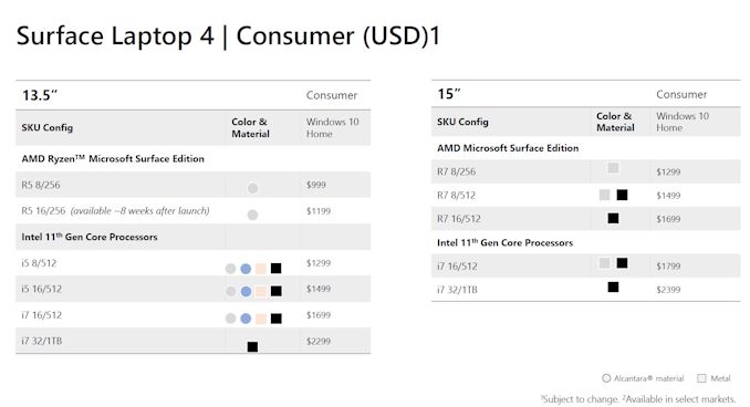
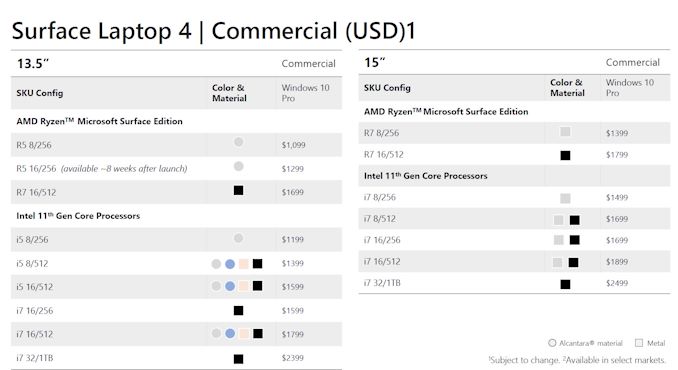
Foundries started limited usage of extreme ultraviolet (EUV) lithography for high-volume manufacturing (HVM) of chips in 2019. At the time, ASML’s Twinscan NXE scanners were good enough for production, but the full EUV ecosystem was not quite there. One of the things that impacted EUV was the lack of protective pellicles for photomasks, which limited usage of EUV tools and affected yields. Fortunately, the situation with pellicles has finally improved thanks to the recent introduction of production-ready EUV pellicles, and matters promise to get even better in the coming years.


Protecting Precious Reticles


ASML has made a great progress with its Twinscan NXE EUV lithography tools in the recent years, improving performance of light source, availability time, and productivity. Its industry peers have also done a lot to make high-volume manufacturing (HVM) using EUV equipment possible. Still, the EUV ecosystem needs to develop further. One of the most notorious challenges the semiconductor supply chain faced with EUV is development of pellicles that were not available two years ago, which is why TSMC and Samsung Foundry had to invent ways how to use their EUV scanners without protective films.


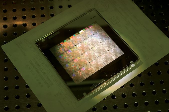
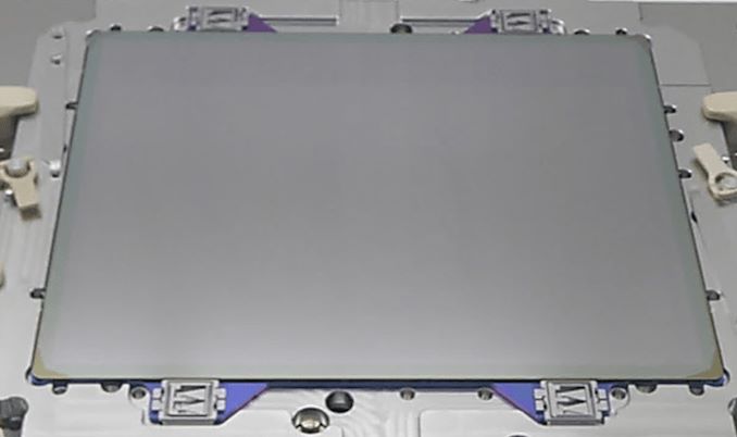
For Reference: A 16nm TSMC Pellicle With Reticle


Pellicles protect 6×6-inch photomasks (reticles) during the chip production flow by sealing them away from particles that could land on their surface, which would otherwise damage them or introduce defects to wafers in production. Each reticle for an EUV tool costs $300,000, so chipmakers are eager to protect them against damage by particles or even the EUV radiation itself as this lowers their costs. Meanwhile, reducing risks associated with yields is perhaps even more important.


The need for pellicles, in turn, varies depending on the manufacturer and the types of photomasks employed. Intel, which is known for its big CPU dies, tends to use single-die reticles, which means that just one mask defect introduced by a particle automatically kills the whole die. Meanwhile, if a 25-die photomask is used, a particle adder will ‘only’ result in 4% lower yield (one dead die), which is why it’s been possible to get away without pellicles for smaller chips and multi-die photomasks.


ASML Leading the Pack. For Now


The industry started to develop protective films for EUV tools relatively late after it transpired that nobody can guarantee that an ultra-complex EUV scanner is 100% free of harmful particles, which is why they were not ready in 2019.


Pellicles for photomasks to be used with deep ultraviolet (DUV) lithography equipment are common and cheap. By contrast, since photomasks for EUV are different from photomasks for DUV (EUV masks are essentially 250 to 350-nm thick stacks featuring 40 to 50 alternating layers of silicon and molybdenum on a substrate), pellicles for such reticles are also quite different. In particular, the very short wavelength of EUV means that pellicles for it have a number of requirements that make them uneasy to produce and expensive. EUV pellicles have to be extremely thin, should not affect reflection characteristics of reticles, should feature a high transmission rate (the higher the rate, the higher is productivity of a scanner), should sustain high EUV power levels, and withstand extreme temperatures (from 600ºC to 1,000ºC in the future).


ASML’s EUV Pellicle (Image Credit: Semiconductor Engineering)


“Most materials absorb very strongly at the more energetic 13.5nm EUV wavelength and, even when the most EUV-transparent materials are selected, the membranes must be extremely thin to approach 90% transmittance,” said Emily Gallagher, a principal member of technical staff at Imec. “Such thin membranes are not usually capable of maintaining sufficient strength to be free-standing at the required dimensions. Additionally, the EUV scanner environment is not compatible with many materials and will subject the pellicle to pump-vent cycles.”


To date, a number of EUV pellicle options have emerged, according to SemiEngineering:


  • ASML introduced its first EUV pellicles in 2019 and licensed the technology to Mitsui Chemicals, which intends to start their volume sales in Q2 2021. Since then, ASML has improved its pellicles.
  • Imec has disclosed test results of its pellicles based on carbon nanotubes.
  • Graphene Square, Freudenberg Sealing Technologies (FST), and some universities are developing their own pellicles.


So far, only ASML has managed to create commercially viable pellicles for EUV tools that are actually available. ASML’s pellicles are based on polysilicon that is 50 nm thick. Back in 2016, they demonstrated a 78% transmissions rate on a simulated 175W source. Currently ASML can sell a pellicle with an 88% transmission rate. And shortly, Mitsui will start supplying such pellicles in volume.


ASML’s latest prototypes made of metal silicide demonstrate a 90.6% transmission rate with 0.2% non-uniformities and less than 0.005% reflectivity on a 400W source.


“This upgrade supports our roadmap, which eventually will take source power up to 400 Watts,” said Raymond Maas, ASML’s product manager for pellicles, in an interview with Bits&Chips.nl. “The pellicle heats up to 600ºC at that power level, which the polysilicon couldn’t withstand.”


By contrast, Imec’s prototype pellicles have a transmission rate of 97.7%. In fact, in the long term, when more advanced light sources are available, more sophisticated pellicles will be needed and this is where Imec’s carbon nanotubes-based pellicles will come into play.


“Few materials have the potential of high EUV transmission beyond 90% and even fewer materials are at the same time compatible with EUV powers beyond 600W. In addition, the pellicle needs to be strong to be suspended over a large area of the mask (~110mm x 140mm),” said Joost Bekaert, a researcher from Imec.


Unfortunately, it is unclear when Imec’s carbon nanotube-based pellicles will be ready for primetime.


Summary


TSMC and Samsung Foundry have invented ways to use EUV lithography tools without pellicles on multi-die photomasks for smaller chips, but such methods are risky as any particle adder can become a yield killing defect. Furthermore, such methods are risky for bigger chips and single-die photomasks, so pellicles are critical for enabling large dies to be made with EUV tools. That said, regardless of the photomask size, pellicles are needed to improve EUV yields and reduce risks across the board.


Overall then, the use of and improvements in EUV pellicles will be a gradual process. The initial pellicles developed and made by ASML and soon to be made by Mitsui are good enough for some of today’s needs, but there is room for improvement with their transmission levels, as evidenced by the next-generation prototypes developed by ASML and Imec. Better pellicles will be needed to account for future scanners as well, since those machines will have more powerful sources. Nonetheless, since such pellicles have a number of indisputable advantages, they are going to be used by chipmakers as they can help to improve yields even at the cost of some productivity.


Source: AnandTech – EUV Pellicles Ready For Fabs, Expected to Boost Chip Yields and Sizes

Computex 2021 Physical Show Cancelled; Virtual Event Still Taking Place

When it comes to technology tradeshows, one of the biggest early victims of the coronavirus outbreak was Computex, the annual PC-centric trade show in Taiwan. After the 2020 show was delayed and then canceled entirely, event organizer TAITRA vowed to come back with a proper tradeshow in 2021. However, even with vaccinations well underway, it’s become clear that it’s not going to be possible to hold the physical show this year either. As a result, the physical Computex tradeshow has once again been cancelled.


In a very brief news release, TAITRA noted that with the pandemic still ongoing, and border controls preventing international travel, it would not be possible to hold the show in 2021.


With another wave of coronavirus pandemic across the world, it doesn’t look like we are close to the end. The majority of the show’s stakeholders, including international exhibitors, visitors, and media, cannot join the show due to border control. Therefore, the organizers of COMPUTEX have decided to cancel the onsite exhibition this year.


The silver lining, at least, is that while the physical show TAITRA wanted to hold won’t be happening, their parallel virtual show, #COMPUTEXVirtual, will continue on as planned. Scheduled to run for a full month, from May 31st to June 30th, #COMPUTEXVirtual will be the show’s first attempt at doing a large-scale virtual event. The virtual show was originally scheduled to run alongside the physical show, but now with the physical show cancelled, it has become the de facto plan B. At this point it’s not clear who will be presenting and what with the virtual show, and undoubtedly vendors and organizers are scrambling to draw up new plans in light of the physical show’s cancellation.


None the less, even a virtual Computex could stand to be a major show. With a strong and ongoing demand for electronics, the lack of a 2020 show, and CES 2021 being a relatively modest event earlier this year, vendors have been eager to roll out new products – and to do so in front of an audience. So we’ll see how things pan out over the next two months.


Source: AnandTech – Computex 2021 Physical Show Cancelled; Virtual Event Still Taking Place

Kingston Introduces NV1 Entry-Level NVMe SSD

As previewed at CES, Kingston’s newest entry-level consumer NVMe SSD is now shipping. The new NV1 uses a similar strategy to Kingston’s entry-level SATA drives like the A400, where Kingston is not guaranteeing a specific set of internal components and expects to mix controllers and NAND to hit the cheapest price points. That results in very conservative performance and endurance specifications: sequential transfers around 2GB/s and endurance ratings around 0.2 DWPD for three years.


Kingston NV1 SSD Specifications
Capacity 500 GB 1 TB 2 TB
Form Factor M.2 2280 PCIe 3.0 x4
Sequential Read (MB/s) 2100
Sequential Write (MB/s) 1700
Warranty 3 years
Write Endurance 120 TB

0.2 DWPD
240 TB

0.2 DWPD
480 TB

0.2 DWPD
Launch Price $63.70

(13¢/GB)
$115.70

(12¢/GB)
$224.90

(11¢/GB)


The Kingston NV1 uses DRAMless SSD controllers like the Phison E13T and Silicon Motion SM2263XT, which are both getting a bit old but are still sufficient to offer a step up from SATA performance. The NAND will tend to be TLC on the smaller capacities and QLC for at least the 2TB model, but realistically Kingston could use either type of NAND on any of the capacities depending on what kind of leftover NAND they have lying around.


The NV1 is a more low-end drive than Kingston’s existing A2000 NVMe SSD, which uses TLC NAND and has DRAM, but uses the 4-channel SM2263 controller. The NV1 does reflect the market’s shift toward higher capacities, with the product line starting at 500GB and going up to 2TB. We expect retail prices for the NV1 will end up cheaper than the A2000, but for the moment the pricing direct from Kingston is only marginally cheaper.


Source: AnandTech – Kingston Introduces NV1 Entry-Level NVMe SSD