Intel Licenses SiFive’s Portfolio for Intel Foundry Services on 7nm

Today’s announcement from SiFive comes in two parts; this part is significant as it recognizes that Intel will be enabling SiFive’s IP portfolio on its 7nm manufacturing process for upcoming foundry customers. We are expecting Intel to offer a wide variety of its own IP, such as some of the x86 cores, memory controllers, PCIe controllers, and accelerators, however the depth of its third party IP support has not been fully established at this point. SiFive’s IP is the first (we believe) official confirmation of specific IP that will be supported.


Source: AnandTech – Intel Licenses SiFive’s Portfolio for Intel Foundry Services on 7nm

AMD Moves GCN 1, 2, & 3-based GPUs and APUs To Legacy; Also Drops Win7 Support

Alongside today’s release of their new Radeon Software Adrenalin 21.6.1 driver – the first to bring support for FidelityFX Super Resolution tech – AMD is also using this opportunity to clean house on supported graphics products. As announced in a new blog post and effective immediately, AMD is moving all of its 1st, 2nd, and 3rd generation Graphics Core Next (GCN) based GPUs and APUs to legacy status. As a result, pre-RX 400 series video cards and pre-Ryzen APUs are no longer supported by AMD’s current drivers, and AMD’s previous 21.5.2 driver set will be the final release for those products. 21.5.2 will also be the final driver that supports Windows 7, as AMD is also using this opportunity to drop support for that already-retired OS.


This week’s change in support marks the first time since 2015 that AMD has moved any video hardware to legacy support. At the time, the company retired its pre-GCN hardware, leaving AMD’s GCN-based Radeon HD 7000 series and newer products as their support baseline. And, after nearly 10 years of support for the oldest pieces of GCN hardware – the then-revolutionary Radeon HD 7970 was launched at the very start of 2012 – AMD is finally winding down support for the first couple of waves of GCN hardware.


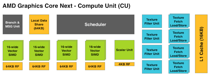
First introduced in 2011, GCN was a major overhaul of AMD’s graphics architecture, moving from an ILP-centric design to a more modern and compute-friendly TLP-centric design. GCN itself has since been supplanted by the RDNA family, but many of the basic design principles of GCN are still alive today in AMD’s enterprise compute-focused CDNA architecture.


As for this week’s product support changes, AMD is essentially retiring all graphics hardware – GPU and APU – that pre-dates 2016’s Polaris (GCN 4) architecture. Consequently, AMD’s lengthy legacy list includes the Radeon 7000 and 8000 series, as well as the 200, 300, and Fury series. Even a few pieces of mobile-focused M400 hardware are on there, since those low-end parts were based on older GCN chips. Overall, this marks a roughly 5-year span of hardware being retired this week, with the youngest parts just turning 5.


On the APU front, the legacy list includes several of AMD’s popular pre-Ryzen APUs, including Bristol Ridge, Carrizo, and Kaveri, which were predominantly sold under the AMD A-series moniker (e.g. A10-9700). It’s worth noting that the resulting support window for these products does end up being a bit shorter than the discrete GPUs, since AMD didn’t release their first Ryzen + Vega APUs until 2018.


The Dearly Departed
Desktop Mobile
AMD A-Series APUs with Radeon R4, R5, R6, or R7 Graphics AMD A-Series PRO processors with Radeon Graphics
AMD Pro A-Series APUs with Radeon R5 or R7 Graphics AMD FX-Series APUs with Radeon R7 Graphics
AMD Athlon Series APUs with Radeon R3 Graphics AMD E-Series APUs with Radeon R2 Graphics
AMD Sempron Series APUs with Radeon R3 Graphics AMD Radeon R7 M400 Series Graphics
AMD Radeon R9 Fury Series, R9 Nano Series Graphics AMD Radeon R9 M300 Series Graphics
AMD Radeon R9 300 Series Graphics AMD Radeon R7 M300 Series Graphics
AMD Radeon R9 200 Series Graphics AMD Radeon R5 M300 Series Graphics
AMD Radeon R7 300 Series Graphics AMD Radeon R9 M200 Series Graphics
AMD Radeon R7 200 Series Graphics AMD Radeon R7 M200 Series Graphics
AMD Radeon R5 300 Series Graphics AMD Radeon R5 M200 Series Graphics
AMD Radeon R5 200 Series Graphics AMD Radeon HD 8500M – HD 8900M Series Graphics
AMD Radeon HD 8500 – HD 8900 Series Graphics AMD Radeon HD 7700M – HD 7900M Series Graphics
AMD Radeon HD 7700 – HD 7900 Series Graphics  


As things stand, I’m not surprised to see AMD lump together GCN 1/2/3 from a driver support standpoint. Despite some very material architecture tweaks among those successive generations, from a product development standpoint they all represent one extended product family, as AMD introduced and replaced GPUs in a piecemeal fashion. Combined with the fact that AMD continued using early GCN parts in newer cards for years, it wasn’t until Polaris in 2016 that AMD finally executed a complete top-to-bottom refresh of its entire GPU product stack. In other words, GCN 1/2/3 are being retired in the same way they lived: together.


Otherwise, as previously mentioned, AMD is also using this opportunity to retire support for their last pre-Windows 10 OS. Like most other hardware vendors, AMD had opted to continue developing drivers for Windows 7 even after the OS itself was retired at the start of 2020, owing to the fact that it was still seeing significant use in some locales. But, after another 18 months of extended support, Windows 7 support is also being dropped. As of today’s 21.6.1 drivers, the only versions of Windows supported are 64-bit editions of Windows 10.


For their part, AMD’s blog post on the retirement notes that “This change enables AMD to dedicate valuable engineering resources to developing new features and enhancements for graphics products based on our latest graphics architectures.” It’s also worth noting that this announcement comes less than 2 weeks after NVIDIA’s own legacy announcement, where the company announced that the similarly aged Kepler architecture will be moved to legacy status later this summer.


Closing out support for all these legacy products then will be AMD’s 21.5.2 driver. The company has posted a fresh “legacy” version of the driver just for these retired products, though it doesn’t look like there’s anything new versus AMD’s existing drivers. According to the company, there are no further driver released planned, and the announcement makes no mention of a security update support period.


Overall, AMD’s early GCN architecture parts marked an important transition for AMD, and the resulting hardware, for all of its merits and weaknesses, kept AMD in the game during a very tough period for the company. So for GCN 1, 2, and 3, this is a retirement that’s well-earned.


Source: AnandTech – AMD Moves GCN 1, 2, & 3-based GPUs and APUs To Legacy; Also Drops Win7 Support

GlobalFoundries To Build New 450K Wafer-per-Year Fab in Singapore

Looking to capitalize on the ongoing chip crunch, GlobalFoundries this morning is announcing that the company is building a new chip fab in Singapore, with the groundbreaking taking place immediately. The unnamed fab will be joining the company’s existing cluster of fabs in Singapore, and once fully ramped up in late 2023, will be capable of processing 450K 300mm wafers per year. The fab is the first of a larger, three phase plan for the foundry, which with investments from customers and the Singapore government, will be spending $4 billion to construct the new fab.


Like the rest of the chip lithography industry, GlobalFoundries is currently enjoying a booming market where they can’t make chips fast enough to satisfy customer demand. Even with multiple fabs located in Singapore, Dresden, and the US, the company is running at capacity and could be selling more chips if they could make them. To that end, the company is preparing to make the first of several planned capacity expansions, starting with its fab cluster in Singapore.


Keeping in line with GlobalFoundries’ pivot towards more specialized processes for specific classes of chips, the new fab is going to be focused on larger process nodes. GloFo is principally investing in capacity for their automotive, 5G mobility and secure device customers, which means adding capacity for their 55nm BiCMOS process for RF, as well as their 40nm processes for embedded memory and RF. A small part of the fab’s capacity is also being set aside for 90nm. And, since this fab is being built with modern tools, the company is being quick to emphasize that these allocations aren’t static, and that many of their tools are fungible, allowing them to be moved between different lines as dictated by demand.


Owing to the unique processes being employed and the overall chip crunch – which even after it diminishes isn’t expected to fully abate any time soon – GloFo is fast-tracking the development of this new fab. With construction already underway (and the formal groundbreaking set for today), the company expects the fab to produce its first commercial wafers in early 2023, only around 18 months from now. And by the time the fab is fully ramped up at the end of 2023, the 250,000 square feet of clean room space will be capable of processing 450K wafers per year (~38K/month). Overall, this marks a nearly 50% increase in GloFo Singapore’s capacity, bringing the total capacity for operations there to 1.5M 300mm wafers per year.


Funding for the $4 billion fab, in turn, is coming from a few sources. According to GlobalFoundries, part of the funding for the fab is coming directly from customers, who are pre-paying for the capacity. As well, Singapore’s Economic Development Board is being listed as a partner. And finally, with GlobalFoundries easily turning a profit, the company has much easier access to loans and other forms of borrowing than it has in previous years.


Overall, this marks the next step in an important turnaround for the contract fab, which was spun-off from AMD almost 13 years ago. Though GlobalFoundries’ plans to compete as a bleeding-edge fab eventually fell to the wayside thanks to the ever-increasing costs of R&D, the company has found a new role as a large-scale provider of older and more specialized manufacturing processes. As a result, GloFo is finally a financially successful chip fab, and with that success comes the need to expand. Once finished, the new Singapore fab will be the first brand-new (and not acquired) fab to be built by the company in several years.


Meanwhile, Singapore is just the first of several planned additions for the contract chip fab. Mindful of the current political climate and every major nation’s desire to secure local chip manufacturing capacity, the company is aiming to expand capacity in all three of its fab sites, ideally splitting capacity equally between Singapore, the US, and Dresden. Singapore, in turn, has become the first major expansion on the basis of need – it’s the oldest fab complex and the first to run out of room – but it won’t be the last. GloFo is already in the middle of its previously-announced $1.4B capacity expansion across all of its sites, and the company wants to invest upwards of 6 billion dollars more over the next couple of years. So, as GlobalFoundries’ fortunes continue to rise, so will the additional fab capacity needed to support the company.


Source: AnandTech – GlobalFoundries To Build New 450K Wafer-per-Year Fab in Singapore

Mobile Flagship Phone Cameras 2021 H1 Review: Megapixels & Telephotos

It’s been well over a year now since our last extensive camera round-up article, and it’s also been a few months now since the release of most of 2021’s flagship device releases, and it’s time to take a snapshot of the current smartphone photography landscape.


Source: AnandTech – Mobile Flagship Phone Cameras 2021 H1 Review: Megapixels & Telephotos

DIY on Intel Ice Lake Xeon Just Got A Little Closer

Since the launch of Intel’s Third Generation Xeon Scalable Ice Lake processors in April, it was widely expected that the initial volumes of hardware would be going towards Intel’s biggest customers through their OEM partners. Users who want retail hardware would have to wait a while, although exactly how long was a bit of a mystery. The answer to this seems to be that Ice Lake Xeon hardware is now available at retail: both motherboards and a CPU or two.


Source: AnandTech – DIY on Intel Ice Lake Xeon Just Got A Little Closer

An AnandTech Interview with Jim Keller: 'The Laziest Person at Tesla'

I’ve spoken about Jim Keller many times on AnandTech. In the world of semiconductor design, his name draws attention, simply by the number of large successful projects he has worked on, or led, that have created billions of dollars of revenue for those respective companies. His career spans DEC, AMD, SiByte, Broadcom, PA Semi, Apple, AMD (again), Tesla, Intel, and now he is at Tenstorrent as CTO, developing the next generation of scalable AI hardware. Jim’s work ethic has often been described as ‘enjoying a challenge’, and over the years when I’ve spoken to him, he always wants to make sure that what he is doing is important in the global context. Today we’re publishing a transcript of a recent chat with Jim, now five months into his role at Tenstorrent, but moreso to talk about Jim the person, rather than simply Jim the engineer.


Source: AnandTech – An AnandTech Interview with Jim Keller: ‘The Laziest Person at Tesla’

Google Announces AMD Milan-based Cloud Instances – Out with SMT vCPUs?

Today Google is announcing a new Cloud instance based on AMD Milan – but beyond the new hardware, it’s really what’s behind the new performance numbers which is what should shake the cloud system – is Google abandoning SMT vCPUs?


Source: AnandTech – Google Announces AMD Milan-based Cloud Instances – Out with SMT vCPUs?

SPEC Updates SERT Suite for ISO-Compliant Server Energy Efficiency Benchmarking

The Standard Performance Evaluation Corporation’s SPEC SERT Suite has evolved as the industry-standard for measuring the energy efficiency of servers over the last decade. Regulatory authorities such as the U.S EPA and Japan’s METI are some of the many who have adopted the suite to determine thresholds for various energy-efficiency programs.


In August 2020, the International Organization for Standardization (ISO) published the ISO/IEC 21836:2020 standard to specify the measurement methodology for assessment and reporting of a server’s energy efficiency. Today, SPEC is announcing SERT Suite 2.0.4, an update to enable its incorporation into the ISO standard. It must be noted that the SERT suite was already compliant with ISO 21836. The new version also brings in ISO compliance report links. In addition to including latest PTDaemon software (v1.9.2) that interfaces with SPEC-approved power analyzers and temperature sensors, and GUI optimizations, the SPEC SERT Suite 2.0.4 also supports servers based on the latest ARM processors from Ampere, Fujitsu, and Marvell.


The SERT 2.0.4 suite is priced at USD 2800, and is available for immediate download. Being a minor version update, it is free for SERT 2 licensees to upgrade. Similar to all other benchmarks developed by SPEC, the SERT Suite from the SPECpower Committee has been developed in a vendor-agnostic manner with representatives from across the industry. Needless to say, this greatly increases the credibility of the benchmark. The SERT Suite allows consumers / cloud service providers to determine the energy efficiency (and, the TCO indirectly) of a particular offering for their workloads. The latest offering keeps up with the evolving industry requirements.


Source: AnandTech – SPEC Updates SERT Suite for ISO-Compliant Server Energy Efficiency Benchmarking

Razer Announces Ultra-Compact "Razer GaN" 130W USB Type-C Charger

Alongside their new AMD-powered Blade 14 laptop, Razer today also used E3 2021 to announce a new, high-powered USB-C charger. The Razer GaN USB Type-C charger is a compact charging solution that is pocket-sized and can deliver up to 130 W of combined charging power across its two USB-C and two USB-A outputs.


If you’ve ever owned one of the latest smartphones or Bluetooth 5.1 devices, it’s likely to come with a USB Type-C charging port. The Type-C connector has become more popular as more and more powered devices come with Type-C. With the USB-IF announcing its specifications for the new USB-PD standard with support for up to 240 W, power supply engineers are increasingly using Gallium Nitride (GaN) semiconductors for more efficient and compact designs.


GaN by name and GaN by nature, the Razer GaN is powered by using Gallium Nitride, which has allowed Razer to cut down on the size of the charger. Razer claims that their GaN charger is small enough to fit inside a pocket, measuring 7.7 x 3.2 x 6.2 mm (W x D x H) in size with a weight of 349 g. Looking at the aesthetics, the GaN includes a black plastic chassis with Razer’s trademark green accent color being used in the USB Type-A ports as well as the power indicator light. And in case you’re still not sure who made it, there’s a Razer logo embossed onto the side as well.


The Razer GaN has a foldable fork for plugging directly into a plug socket and comes supplied with global power adapters. Users can charge devices in regions such as North America, Europe, the UK, and Asia. Also included in the accessories is a 2 meter USB cable, although Razer didn’t specify Type-C or Type-A.


In terms of charging ports, the Razer GaN has two Type-C outputs and two Type-A outputs. Each pair of outputs are on a shared power plane, allowing the charger to power several devices at once, though at a reduced rate if used with multiple high-powered devices. This works out to the two Type-C ports sharing 100 W of capacity, while the two Type-A ports share another 18 W. And since this is a universal power supply, the Razer GaN can charge everything from phone and tablets to Razer Blade laptops, Apple MacBooks, as well as smartwatches and Windows laptops that support Type-C charging. 


Razer GaN Charger
  Max Port Power Max Group Power Max Charger Power
USB-C #1 100W 100W 130W
USB-C #2 100W
USB-A #1 18W 18W
USB-A #2 18W


The Razer GaN USB Type-C 130 W charger can be pre-ordered at the Razer Store from the 14th of June, with shipping of stock expected within 30 days of the date. Though don’t mistake the diminutive size of the charger for a diminutive price tag; the charger carries an MSRP of $180.


Source: AnandTech – Razer Announces Ultra-Compact “Razer GaN” 130W USB Type-C Charger

Razer Unleashes Blade 14 Gaming Laptop: Ryzen 5000 Mobile with GeForce Graphics

During their E3 2021 gaming event this afternoon, Razer has launched the latest variant of its popular Blade 14 gaming laptop. For the first time, Razer is using an AMD processor to power its latest Blade 14 thin gaming laptop. Marking a milestone within the company, the Razer Blade includes plenty of features, including Wi-Fi 6E, dual USB 3.2 G2 Type-C, and multiple options with NVIDIA’s GeForce RTX graphics for fine-tuning the laptop’s portable gaming performance.


Back in 2011, when Razer first entered the gaming laptop market, the competition between Intel and AMD in the desktop and mobile space wasn’t like it is now. Since then, a lot has changed with the emergence of AMD’s Ryzen architecture, and at present, it is doing very well. With Ryzen Mobile offering powerful performance and in January, it launched its Ryzen 5000 Mobile parts at CES 2021.


With Razer commanding a niche market in the laptop space with all of its models designed for gaming, the latest Razer Blade 14 comes equipped with AMD’s Ryzen 9 5900HX processor, with eight cores, sixteen threads, a maximum boost clock speed of 4.6 GHz, and is unlocked allowing users to apply overclocks. While the Blade 14 isn’t an ‘AMD Advantage’ system benefiting from both AMD processor and graphics, it marks a big step for a brand typically associated specifically with Intel chips. 


The AMD Ryzen powered Razer Blade 14 comes with two choices in regards to panel type. This includes the option of a 1080p 144 Hz 100% sRGB display, or a more premium 1440p 165 Hz 100% DCI-P3 display. Both panels are IPS-based and come with variable refresh rate support. For storage, the Razer Blade 14 includes a 1 TB PCIe 3.0 x4 NVMe SSD, while memory comes in the form of 16 GB of DDR4-3200. Unfortunately for buyers looking at later-life upgrades, the memory is fixed onto the motherboard, so 16 GB is all it ever will have.


Buyers can select between three NVIDIA options in terms of graphics. This includes a GeForce RTX 3060 mobile GPU with 6 GB of VRAM, an RTX 3070 with 8 GB of VRAM, or an RTX 3080 also with 8 GB of VRAM. All three models have their GPUs set to 100 W TGP (total graphics power). Keeping the components cool is a vapor chamber cooling solution, and Razer is advertising up to 12-hours battery life and comes with a compact 230 W power adapter.


Razer is also touting the Blade 14 as the world’s thinnest gaming laptop, and the dimensions make it rather sleek indeed. It’s 16.8 mm thick, with a 220 mm x 319.7 mm footprint. Although Razer didn’t provide us with details on the weight, the frame itself is custom CNC milled from a single block of T6 grade aluminum, commonly used for aircraft parts, and comes with a matte black anodized finish. Other design aspects include per-RGB backlit keys powered by Razer Chroma and features an N-Key rollover keyboard. The keys themselves have a 1 mm actuation, and keys can be programmed via Razer Synapse 3. Also included is a large glass precision trackpad, which is Windows Precision-capable and adapts to usage and can respond to multiple finger gestures. 


I/O connectivity include two USB 3.2 G2 Type-C ports with DP alt-mode and 100 W charging capabilities, two USB 3.2 G2 Type-A ports, one HDMI 2.1 video output, and a single 3.5 mm combo audio port. Along the top of the bezel is a Windows Hello 720p webcam and comes with THX-certified Spatial Audio with two premium speakers. The Blade 14 also comes with a Kensington lock for security on the go.


The AMD Ryzen 5900HX powered Razer Blade 14 will start shipping from June 14th, with prices starting at $1799.


Related Reading


Source: AnandTech – Razer Unleashes Blade 14 Gaming Laptop: Ryzen 5000 Mobile with GeForce Graphics

Sponsored Post: Keep Your App’s Memory Safe with Arm Memory Tagging Extension (MTE)

Subtle memory bugs, including buffer overruns and pointer errors, create ticking time bombs inside your applications. Malicious actors can exploit these bugs to execute unauthorized code, take over systems to add them to malware botnets, or simply cause applications and systems to crash. The notorious Morris Worm of 1988 was one of the earliest examples of a malicious application exploiting a buffer overflow. Announcements of memory safety issues creating potential exploits arrive with alarming frequency, either from security researchers or found loose in the wild.


The impact on users can be substantial. Rogue applications can take advantage of unsafe memory in order to gain access to sniff out sensitive data, such as user credentials and passwords, enabling access to higher levels of privilege in the system. This allows bad actors to gain access to confidential data or make the system part of a larger botnet. It’s not always outside forces that cause problems – sometimes unsafe memory results in unpredictable system crashes due to memory leaks and related issues, frustrating users. It’s estimated that two-thirds of all Android vulnerabilities happen due to unsafe memory practices.


Arm Memory Tagging Extension


Software-based solutions, including Address Sanitizer (Asan), help mitigate these memory issues by integrating memory corruption detection into modern compilers. However, Asan requires adding software instrumentation to application code, which can significantly slow down app runtime and increase memory usage, particularly problematic in mobile and embedded systems.


What’s needed is a solution to detect and minimize memory bugs with minimal impact on performance and memory use. Properly implementing a hardware-based method for detecting potentially unsafe memory usage results in smaller memory usage and better performance, while improving system reliability and security.


Arm introduced its memory tagging extension as a part of the Armv8.5 instruction set. MTE is now built into Armv9 compliant CPUs recently announced by Arm, such as the Cortex-X2, Cortex-A710, and Cortex-A510. Future CPUs based on Armv9 will also integrate MTE. These all include memory tagging as a basic part of the architecture.


Source: AnandTech – Sponsored Post: Keep Your App’s Memory Safe with Arm Memory Tagging Extension (MTE)

Seagate Signs HAMR Deal with Showa Denko: Secures Second Source for HAMR Platters

Seagate this week signed an agreement with Showa Denko in a bid to secure a second source of platters for its hard drives based on heat assisted magnetic recording (HAMR) technology. Under the terms of the deal, Seagate will evaluate SDK’s existing materials for HAMR media and the two companies will jointly develop future materials. 


Seagate started to ship its Exos HDDs featuring HAMR inside its Lyve storage systems late last year. These hard drives use key components, such as recording heads with a near field transducer that heats up the media as well as glass platters with an FePt magnetic layer, developed and made entirely in-house. Being a vertically integrated company, Seagate has enough production capacities to continue building platters for HAMR drives internally, but having a second source for a crucially important component makes a lot of sense for high-volume products. 


Having spent over 10 years on HAMR pathfinding and research, Showa Denko formally began to develop its glass platters for HAMR HDDs in February, 2020. Back then, the company said that HAMR would achieve areal density of 5-6 Tb/in2 in the future, enabling 3.5-inch hard drives with eight or nine platters to store 70 TB – 80 TB of data. 


By now, Showa Denko has finished development of its first HAMR media material featuring a FePt magnetic alloy and technology to mass-produce hard drive platters. Under the terms of the agreement between SDK and Seagate, the hard drive maker will evaluate the material designed by the Japanese company. Going forward, Seagate and SDK will jointly develop new magnetic alloys for HAMR HDDs.


For now, Seagate will continue using its own FePt glass media inside its HAMR HDDs, but if it finds Showa Denko’s HAMR media good enough, it might use it for future hard drives.


The contract between Seagate and Showa Denko ensures that the hard drive maker will have two sources of HAMR platters in the future, which will be important if Seagate significantly expands usage of its HAMR technology. In fact, once HAMR media hits certain areal density (i.e., significantly higher than PMR’s 1.14 Tb/inch2), it will make a great sense to adopt the technology nor only for highest-capacity HDDs, but also for midrange HDDs to cut down their costs.


“[HAMR] is not only about the highest capacity point,” said David Mosley, CEO of Seagate, at a conference last year. “If we can save a disk and two heads in a 16 TB drive, we will look at doing that as well. So, it is really across the whole portfolio, which is why we think that this platform play is so important. We can introduce HAMR into the same platform. The cost increases are really nominal.”


Furthermore, Seagate will also ensure that SDK-made HAMR platters will be compatible with its HAMR implementation, which might become the company’s competitive advantage against Toshiba and Western Digital once they adopt this technology.


“We expect this alliance will further accelerate technological development pioneered by the two companies,” a statement by Showa Denko reads.


For Showa Denko, the world’s largest independent maker of HDD platters, it is important to maintain close relationship with all makers of hard drives. Nowadays the bulk of SDK’s shipments are platters designed for PMR and SMR HDDs, but it is also ramping up production of media for Toshiba’s MAMR-based drives. The pact with Seagate ensures that Showa Denko will also be a part of upcoming HAMR HDDs.


Related Reading:


Source: Showa Denko


Source: AnandTech – Seagate Signs HAMR Deal with Showa Denko: Secures Second Source for HAMR Platters

Xilinx Expands Versal AI to the Edge: Helping Solve the Silicon Shortage

Today Xilinx is announcing an expansion to its Versal family, focused specifically on low power and edge devices. Xilinx Versal is the productization of a combination of many different processor technologies: programmable logic gates (FPGAs), Arm cores, fast memory, AI engines, programmable DSPs, hardened memory controllers, and IO – the benefits of all these technologies means that Versal can scale from the high end Premium (launched in 2020), and now down to edge-class devices, all built on TSMC’s 7nm processes. Xilinx’s new Versal AI Edge processors start at 6 W, all the way up to 75 W.


Source: AnandTech – Xilinx Expands Versal AI to the Edge: Helping Solve the Silicon Shortage

An AnandTech Interview with TSMC: Dr. Kevin Zhang and Dr. Maria Marced

In the past week, TSMC ran its 2021 Technology Symposium, covering its latest developments in process node technology designed to improve the performance, costs, and capabilities for its customers. In this event, TSMC discussed its increasing use of Extreme Ultra Violet (EUV) lithography for manufacturing, enabling it to scale down to its 3nm process node, well beyond that of its competitors. TSMC also addressed the current issues surrounding demand for semiconductors, along with announcing that it is building new facilities for advanced packaging production. Joining CEO Dr. CC Wei as part of the keynote presentation was AMD’s CEO Dr. Lisa Su, Qualcomm’s President (and soon to be CEO) Cristiano Amon, and Ambiq’s Founder and CTO Scott Hanson.

As part of the proceedings, TSMC offered AnandTech a 30-minute interview with Dr. Kevin Zhang, SVP of Business Development, and Dr. Maria Marced, President of TSMC EU, as an opportunity to learn more about TSMC’s driving directions as well as cooperation with industry partners.


Source: AnandTech – An AnandTech Interview with TSMC: Dr. Kevin Zhang and Dr. Maria Marced

Computex 2021: G.Skill Trident Z Royal Elite With DDR4-4000 CL14, Tight Latencies

During Computex 2021, G.Skill has announced a couple of new memory kits featuring its regal-looking Trident Z Royal Elite heatsinks. Available with super tight primary latencies of CL14, the new Trident Z Royal Elite kits will be available in DDR4-4000 and DDR4-3600, with various capacities available, including 16, 32, 64, and 128 GB kits.


There are many different parts of a system that can add varying levels of aesthetic glamor, including the motherboard, CPU cooler, fans, anything with RGB on it, but almost everything struggles to be as bling as G.Skills Trident Z Royal Elite memory. Launched back in April, the G.Skill Trident Z Royal Elite comes available in gold and silver. Both color variants feature eight customizable RGB LED lighting zones, with a patented crystalline patterning across for that regal touch.


Touching on the specifications, the top kit features speeds of DDR4-4000 with CL14-14-14-35, at a larger-than-expected operating voltage of 1.55 V. It will be available in two varieties, including a 16 GB (2 x 8 GB), and a 32 GB (2 x 16 GB) kit. The DDR4-3600 kits come with equally tight CL14 latencies, with a slightly lower 1.45 V operating voltage, and will be available in 16 GB (2 x 8 GB), 32 GB with the option for 2 x 16 GB or 4 x 8 GB kits. For users looking for more capacity, there are options at 64 GB with 4 x 16 GB and a large 128 GB kit with 8 x 16 GB. 


G.Skill says the new Trident Z Royal Elite DDR4-4000 and DDR4-3600 CL14 kits will be available from June but haven’t provided us with pricing at the time of writing.


Source: AnandTech – Computex 2021: G.Skill Trident Z Royal Elite With DDR4-4000 CL14, Tight Latencies

Apple Announces iOS 15 and iPadOS 15: The Highlights

Today at Apple’s 2021 WWDC event, the company unveiled the new iOS 15, iPadOS 15 operating systems. This year, Apple presented a large number of new features and improvements across both the main OS components as well as Apple’s core ecosystem apps. While we are just scratching the surface, we picked out a few highlight features that are looking forward to test later in the year once the new versions will be hitting consumers in their final versions.


Source: AnandTech – Apple Announces iOS 15 and iPadOS 15: The Highlights

Computex 2021: TeamGroup Announces its First DDR5-4800 Memory Module

Back in December 2020, TeamGroup announced its intentions for the switch to DDR5 memory on future platforms. During Computex 2021, TeamGroup claims it has ‘successfully taken the lead over competing PCB manufacturers’, with the first of its announced products for DDR5, the Elite DDR5-4800 16 GB module. Back at CES 2021, ADATA claimed that it has a DDR5 module in hand, but it sent us rendered images. We ultimately disapprove of this practice – don’t state you have it in hand until you are ready to provide us actaul photographs of the thing. Unfortunately, TeamGroup has done the same here, providing renders. not photographs.


The Road to DDR5


Over the last year, we’ve highlighted certain aspects of DDR5 memory and what users can expect, including features, memory latency, and technological advancements over the current DDR4 memory. Some of which can be seen below:


TeamGroup’s announcement hasn’t come as a surprise given how long DDR5 has been speculated and discussed over the last year. One of the first platforms to supposedly feature DDR5 support is Intel’s Alder Lake microarchitecture, which is expected to land in Q4 2021/Q1 2022. The first series of DDR5 from TeamGroup will be based on its ‘Elite’ memory series, with the first kit to feature speeds of 4800 MT/s, sub-timings of CL40-40-40-77, and will feature an operating voltage of 1.1 V.


One of the primary features of DDR5 is integrated on-die ECC, which is designed to improve overall system stability (but is actually more to do with yield). This is different to module-wide ECC, which DDR5 does not support by default (you still need a module-wide ECC module to support ECC technology). The information provided by TeamGroup say the Elite DDR5-4800 has double the banks compared to DDR4, with an all-black PCB. It is unclear whether or not the Elite DDR5-4800 will feature heatsinks, or they will operate with a bare PCB. We also know that it will feature 16 GB of capacity and will likely be sold as a dual-channel kit, and perhaps individually.


At present, there’s no information on latency timings or how much the Elite DDR5-4800 16 GB module will cost, but TeamGroup does state that it will be unveiling its ‘new generation’ of products in September 2021.


Source: AnandTech – Computex 2021: TeamGroup Announces its First DDR5-4800 Memory Module

NXZT Announces N7 Z590 Motherboard For Rocket Lake

In July last year, we reviewed NZXT’s N7 Z490 motherboard for Intel’s 10th generation Comet Lake processors. Typically later to the market than other vendor’s key models, NZXT has announced its latest option which aims to benefit from the PCIe 4.0 support in Rocket Lake. Enter the N7 Z590. Some of the features include a full-cover panel across the PCIe slot area, Wi-Fi 6E, 2.5 GbE, dual M.2, support for DDR4-4600 memory, and is advertised with a 14-phase power delivery.


NZXT entered the motherboard market for the first time back in 2018 with the N7 Z370, which we also reviewed. Typically known more for its clean-cut chassis and cooling products, NZXT first tasked the job of providing the PCB and componentry to ECS for the Z370, and then switched to ASRock for Z490. It is unclear which vendor NZXT relies on for the N7 Z590, but we expect the relationship with ASRock is still intact, but we will confirm this when we know.


The N7 Z590 is similar to the previous model in terms of aesthetics, with models available in either matte black or white and uses a full cover PCIe slot armor and more armor covering the right-hand side of the board. Despite not including any integrated RGB LED lighting onboard, NZXT is using its CAM software to control the four RGB LED headers located on the board, with an integrated fan controller adding control of cooling with a total of seven 4-pin headers located on the board.


In terms of specification, the NZXT N7 Z590 has two full-length PCIe slots, one operating at PCIe 4.0 x16 and the other at PCIe 3.0 x4, with three PCIe 3.0 x1 slots. In the top right-hand corner is four memory slots, with support for DDR4-4600 and a total capacity of up to 128 GB. Storage capabilities include two M.2 slots, one featuring support for PCIe 4.0 x4 drives and the second slot supporting PCIe 3.0 x4 and SATA drives. There are four SATA ports for conventional storage and optical devices that also support RAID 0, 1, 5, and 10 arrays.


The rear panel has a much better selection of input and output than the N7 Z490, with one USB 3.2 G2x2 Type-C, three USB 3.2 G2 Type-A, four USB 3.2 G1 Type-A, and two USB 2.0 ports. A Realtek ALC1220 HD audio codec controls the five 3.5 mm audio jacks and S/PDIF optical output, while wireless capability comes from Intel’s latest AX210 Wi-Fi 6E CNVi. Taking care of wired networking is a Realtek RTL8125BG 2.5 GbE controller, while also on the rear panel is an HDMI 2.0 video output and a small clear CMOS button.


The NZXT N7 Z590 is currently available on NZXT’s website for $280.


Source: NZXT


Related Reading


Source: AnandTech – NXZT Announces N7 Z590 Motherboard For Rocket Lake

Noctua NH-P1 Passive CPU Heatsink Spotted at Newegg for $100

Back at Computex 2019, when we visited Noctua at its booth, we saw a concept CPU heatsink, a monolith, with a passive design. In many circles including fans of silent and passively cooled systems, this is a highly anticipated announcement, and although there’s nothing official from Noctua yet, the new NH-P1 has been spotted on a listing at Newegg by FanlessTech.


The Noctua NH-P1 features a completely fanless design, and although there’s no official word on its TDP rating yet, we saw the concept cooler at Computex 2019 keeping an Intel Core i9-9900K cooled in a test system. The 9900K for reference has a PL1 rating of 95 W, and a PL2 rating of 210 W, so we know it has some serious cooling potential for a passive cooler.


The Noctua Concept Fanless CPU Cooler at Computex 2019


As with other Noctua CPU coolers, it includes its SecuFirm2+ mounting system which is compatible with Intel’s LGA1200, LGA115x, and LGA1200xx sockets, and also allows support for AMD’s AM4, AM3+, AM3, AM2, and FM2 sockets. The finer specifics of the design are currently unclear, but Noctua does supply a tube of its latest NT-H2 thermal paste with it, as well as a limited six-year warranty. Noctua doesn’t recommend overclocking due to the limited cooling properties of a passive design, but it can also be used with Noctua’s fans, with grooves that allow users to add fans with its retention brackets.


At the time of writing, Newegg has pulled the listing from its website, which means it could have jumped the gun, but we do expect the Noctua NH-P1 to be announced imminently. The Newegg listing had the Noctua NH-P1 at $100, which means it’s not going to be cheap, but it targets a niche market.


Source: FanlessTech


Source: AnandTech – Noctua NH-P1 Passive CPU Heatsink Spotted at Newegg for 0