Samsung: Deployment of 3nm GAE Node on Track for 2022

Samsung Foundry has made some changes to its plans concerning its 3 nm-class process technologies that use gate-all-around (GAA) transistors, or what Samsung calls its multi-bridge channel field-effect transistors (MBCFETs). Based on new information direct from Samsung, it would appear that its first version of 3nm, 3GAE (3nm gate-all-around early), is coming to high volume manufacturing a year later than expected, but also it seems to have removed this technology from its public roadmap, suggesting it may be for internal use only.


Meanwhile, 3GAE’s successor 3GAP (3nm gate-all-around plus) node is still in the roadmap, it is on track for volume manufacturing in 2023.


3GAE on Track for 2022, Maybe Just Not for Everyone


At its recent Foundry Forum 2021 in China, Samsung Foundry presented its updated public technology roadmap which was then republished by bloggers at Baidu and Weibo.


On its FinFET technologies, both 5LPP and 4LPP nodes are new to the roadmap, and set for high-volume manufacturing (HVM) in 2021 and 2022, respectively.


For GAA technology, 3GAE is absent from the roadmap, but 3GAP is there. We reached out to Samsung and a representative confirmed that the 3GAE technology is still on track for ramp in 2022. From the slide, we can see that MBCFET-based 3GAP will enter its HVM phase sometime in 2023.


“As for the 3GAE process, we’ve been in discussion with customers and expect to mass-produce 3GAE in 2022,” the spokesperson said.


The absence of 3GAE process from the public roadmap may be explained by the fact that it will only be available to Samsung’s own LSI division, just like some other (E)arly nodes. That being said, previous generation (E)arly nodes are still mentioned in the slides that the company demonstrated.


Samsung originally announced its MBCFET-based 3GAE and 3GAP nodes in May 2019. Back then, the company promised a 35% performance increase, a 50% power consumption reduction, and a 45% area reduction for 3GAE compared to 7LPP. Furthermore, the company announced the availability of v0.1 of its 3nm PDK and at the time said that volume production using 3GAE was set to start in late 2021. With that moving to 2022 based on the latest information, one might interpret this as either a delay or miscalculation based on enabling GAA designs at scale.


However on the plus side, Samsung taped out the first 3 nm test chip several weeks ago. It also announced the availability of Synopsys EDA tools compatible with the new fabrication technologies. The use of fabrication processes that rely on brand-new transistors is always a challenge – in addition to new electronic design automation (EDA) tools, chip developers need all-new IP. We look forward to hearing more disclosures on that front.


A New 4LPP Node on FinFETs


While it looks like general customers are not going to use Samsung’s 3 nm nodes until 2023, the newly announced 4LPP is set to meet the requirements of the company’s clients in 2022. Since 4LPP relies on familiar FinFETs, it will be much easier for Samsung’s customers to use this node when compared to any 3nm GAA nodes early in their lifecycle.


It is noteworthy that Samsung now considers its 5 nm and 4 nm-class technologies as different node branches on its slides. Previously, the foundry considered its 4LPE as an evolution of its 7LPP process. Perhaps this is because 4 nm is set to offer very tangible PPAc (power, performance, area, cost) advantages over 5 nm, or because there are substantial internal changes (e.g., new materials, significantly higher usage of extreme ultraviolet lithography, etc.). 


For example, one of Samsung’s slides specifically mentions density and performance improvements for 5LPE and 5LPP, but only mentions power and performance improvements for 4LPP. The overlapping technologies will also help to mitigate risks if one of the nodes does not meet certain expectations.


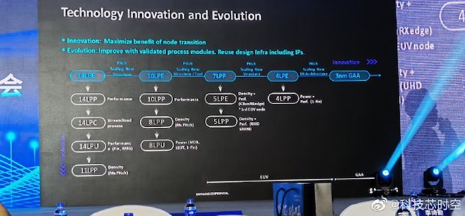
Surprisingly, Samsung Foundry is set to ramp production using its 4LPE and 5LPP technologies at around the same time in 2021, which could enable it to offer different PPAc advantages for different chip designs. 


Summary


While Samsung Foundry’s GAAFET/MBCFET 3 nm plans appear to have changed and slipped by a year, it is unlikely a big problem for the company as its (E)arly nodes were never widely adopted. To cover that additional year, the company’s new 5LPP and 4LPP FinFET-based technologies are set to enable PPA advantages for Samsung Foundry’s clients and enable the company to gain more experience with EUV equipment before using it for its 3GAE/3GAP nodes.


Source: AnandTech – Samsung: Deployment of 3nm GAE Node on Track for 2022

ASUS ROG Maximus XIII Hero Review: Everything for Rocket Lake

On our test bench today is one of ASUS ROG’s mid-range models designed for Intel’s Rocket Lake processors. The ASUS ROG Maximus XIII Hero brings plenty of premium controllers and connectivity to the table including dual 2.5 GbE, dual Thunderbolt 4 Type-C, Wi-Fi 6E, four M.2 slots, and a robust 14-phase power delivery capable of pushing Rocket Lake above its capabilities. We have put the Z590 Hero through its paces to see if it is the champion model in the sub $500 Z590 market.


Source: AnandTech – ASUS ROG Maximus XIII Hero Review: Everything for Rocket Lake

ASUS Announces "Smartphone for Snapdragon Insiders" – A Real Product, or Just A Marketing Showcase?

Today ASUS and Qualcomm are announcing the “Smartphone for Snapdragon Insiders” – a ASUS designed phone with extensive Snapdragon branding – a ROG Phone 5 spin-off, or just a pointless marketing exercise?


Source: AnandTech – ASUS Announces “Smartphone for Snapdragon Insiders” – A Real Product, or Just A Marketing Showcase?

Intel Hybrid CPU Starts 'End of Life' Process

As I opened my inbox this morning, I was surprised. I keep track of when Intel puts products on End of Life (or starts the process through something called Product Discontinuance), and so I usually see a run of 3-5 year old CPUs or storage or servers pass through without much of a worry. When I opened up my daily brief today however, the headline read ‘Core Processor with Hybrid Technology Discontinued’, which immediately struck me as a bit crazy.


Intel announced Lakefield, its only Hybrid CPU on the market, in January 2019. It pairs one of its big cores with four smaller Atom cores in a small 12mm square package. Not only this, Lakefield is one of Intel’s first Foveros packaging processors, with a 10nm compute piece of silicon sitting on top of an IO die, all packaged together with DRAM on top. The goal of the Lakefield design was to produce a processor with a super low idle power, but also have enough performance for hand-held devices. Intel quoted 1.2 mW when in idle, meeting that goal.


Lakefield came to market in June 2020 in two products: the Samsung Galaxy Book S 13.3-inch clamshell laptop, and the Lenovo ThinkPad X1 Fold, a foldable display-based design. Both of these products were premium priced, particularly the Fold with its display, however reported performance was more akin to a quad-core Atom notebook than the $2000 quad-core mobile devices they were aiming for. Battery life sounded good, although we have never tested it at AnandTech due to lack of access to review samples from Samsung, Lenovo, or Intel.


The key thing was the Hybrid CPU design. By pairing one of Intel’s big cores with four of its smaller Tremont Atom cores, the goal was to run the device almost exclusively on the Atom cores for efficiency and then call on the big core when anything latency related was required, such as when the user touches the screen or the keyboard. Within 16 milliseconds (or one frame at 60 Hz), the processor would switch over to the big core for the touch screen interaction, do what it needed to do (often in under 16 ms), and then power back down.


In principle, the concept is sound and makes a lot of sense, especially if the goal is to save battery. As Intel’s first Hybrid CPU design however, there were some initial teething issues as managing threads between the different performance levels required adjustments to Windows’ scheduler. Microsoft already has experience with this when dealing with Windows on Snapdragon devices using the Arm architecture, however it was a first for x86 and the first implementations were reportedly quite rough.


In reality, because of the price of the device, it was compared to hardware that had only big cores. Even if it was compared to Atom based notebooks in the $400 range, because the processor was a low powered device, often lower than the Atom notebooks it was being compared to, it didn’t fall favorably in those benchmarks either. The goal of Lakefield for Intel wasn’t performance, but experience and form factor innovation, which benchmarks never indicate.


The note today from Intel indicates that Lakefield is now on the path to End of Life. This means the following milestones:


  • Start of Product Discontinuance: July 6th 2021
  • Last Corporate Assurance: October 8th 2021
  • Last Product Discontinuance Order: October 22nd 2021
  • Orders are Non-Cancellable from October 22nd 2021
  • Last Shipment Date: April 29th 2022


The start of the process means announcing that they will stop manufacturing processors (July 6th) and if a company wants to put in an order, they have until October 22nd. However that’s also the date where orders can’t be canceled or returned, and all orders will be shipped by April 29th. That means that products could still come out with Lakefield after April 29th, however the OEM partners will not have any means to secure additional stock.


Intel has set its sights on its future Hybrid CPU designs, with the upcoming Alder Lake platform set to launch end of this year in either desktops or notebooks. There is also talk that Windows 11 is better suited to deal with Intel’s hybrid designs from a scheduler perspective. Overall, to see its only public Hybrid CPU suddenly go on product discontinuance after only a year in the market isn’t a great commitment to the technology from OEM partners. Intel’s own Product Change Notification states that ‘market demand for the products listed has shifted to other Intel products’.


Related Reading


Source: AnandTech – Intel Hybrid CPU Starts ‘End of Life’ Process

Intel Continues to Rehire Veterans: At Some Point They’ll Run Out

News on the wire today is that Intel has rehired 28-year veteran Shlomit Weiss into the position of Senior VP and Co-General Manager of Intel’s Design Engineering Group (DEG), a position recently vacated by Uri Frank who left to head up Google’s SoC development. As reported in Tom’s Hardware and confirmed in her own LinkedIn announcement, Weiss will be working at Intel’s Israel design center alongside Sunil Shenoy and is ‘committed to ensure that the company continues to lead in developing chips’. Weiss is the latest in an ever growing list of ‘re-hiring’ Intel veterans, which leads to the problem that at some point Intel will run out of ex-employees to rehire and instead nurture internal talent for those roles.


Source: AnandTech – Intel Continues to Rehire Veterans: At Some Point They’ll Run Out

Cristiano Amon Takes over as Qualcomm CEO: Reiterates Focus on Custom CPUs

As of June 30th, Qualcomm’s Cristiano Amon has taken over as the company’s CEO, replacing his predecessor Steve Mollenkopf which has now retired. In statements to Reuters, Amon had made comments regarding the company’s future CPU roadmap, which come to further contextualise the company’s completed acquisition of NUVIA last March.


Source: AnandTech – Cristiano Amon Takes over as Qualcomm CEO: Reiterates Focus on Custom CPUs

ASUS Launches Zenfone 8 in US: Starting at $599

Following the phone’s initial announcement mid-May, this week ASUS has officially launched their new ZenFone 8 in the US starting at a price of $599. The ZenFone 8 is a bit unusual in the market as it is trying to fit itself in the niche of a small flagship device – at least in terms of performance.


Source: AnandTech – ASUS Launches Zenfone 8 in US: Starting at 9

Micron Sells Lehi 3D XPoint Fab to Texas Instruments for $900M

Back in March of this year, Micron announced that it would be getting out of the 3D XPoint business entirely, abandoning the technology and putting its sole 3D XPoint fab up for sale. Now a short few months later, Micron has secured a buyer for the fab – and it’s not Intel. Rather it will be Texas Instruments who picks up the fab, buying it off of Micron for $900 million with plans to convert it over to analog and embedded processors.


The sale of the Lehi fab is the latest and final chapter in Micron’s years-long efforts to unwind its non-volatile memory joint venture with Intel, IM Flash. Over the last decade Micron has acquired Intel’s share of the business in multiple stages, culminating in acquiring the crown jewel of the former partnership, the Lehi, Utah 3D XPoint fab, in 2018. Since then, Micron decided that it would dissolve its 3D XPoint partnership with Intel entirely, culminating with the company abandoning the technology entirely, leaving Micron with a modern fab that it didn’t have an immediate need for.


To that end, Micron put the fab up for sale earlier this year, and has quickly found a buyer amidst the ongoing chip crunch. And while former partner (and current customer) Intel was the most likely candidate, they were not a shoe-in. As our own Billy Tallis put it at the time “Intel is not guaranteed to be the buyer of the Lehi, UT fab. They’ve doubtless had opportunities to do so before as Intel and Micron unwound their partnership”.


Instead, the memory fab will be going to Texas Instruments, who is buying the building – but not all of the tools. Though designed for 3D XPoint production, the Lehi fab is otherwise a modern, 2 million square foot fab that can process 300mm wafers and is readily capable of being converted to other uses; and this is the direction TI will be taking things. The company is currently planning to equip the fab for the production of analog and embedded processors on the 65nm and 45nm nodes, with the ability to take the fab “beyond those nodes as required.” For Texas Instruments this will be their fourth 300mm fab.


Meanwhile the remaining memory tools that TI isn’t buying will be further assets for Micron, who will be keeping some of them and selling the rest. According to the company’s press release, some of these tools are getting redeployed to other Micron fabs, some have been sold, and yet other tools are still up for sale. Micron doesn’t mention who the tool buyers are, but given the specialized nature of the equipment, it wouldn’t be too surprising if Intel were among them. Overall, Micron is valuing the tools at $600 million, bringing the total value of the transaction to a cool $1.5 billion.


The sale is expected to close at the end of the year, at which point TI will be putting out offers to retain all of the Lehi staff as the fab gets converted over to TI’s analog and logic processes.


Finally, for the sole company to actually use 3D XPoint memory, the sale of the Lehi leaves in question Intel’s own 3D XPoint production plans. Having sold their share of the fab to Micron, Intel transitioned to being a customer of the world’s only 3D XPoint fab in late 2019 – an arrangement that left the fab operating in the red for Micron, as Intel’s 3D XPoint orders weren’t enough to fully utilize the fab. IM Flash jointly developed Intel’s current (second-generation) 3D XPoint memory technology as well, and it’s believed that the Lehi fab has been producing all of that memory for Intel.


So it remains to be seen just how Intel will be impacted, as the sale puts a running clock on how much longer they can buy 3D XPoint memory from the third-party fab. Eventually Intel will need to setup their own fab – likely in Rio Rancho, NM, where their 3D XPoint R&D takes place – but so far the company hasn’t announced any such plans.


Sources: Texas Instruments, Micron


Source: AnandTech – Micron Sells Lehi 3D XPoint Fab to Texas Instruments for 0M

Update on Intel Sapphire Rapids in 2022: Q1 for Production, Q2 for Ramp, H1 Launch

In the news cycle today, Intel is announcing an update to its planned deployment of its next generation Xeon Scalable platform known as Sapphire Rapids. Sapphire Rapids is the main platform behind the upcoming Aurora supercomputer, and set to feature support for leading edge technologies such as DDR5, PCIe 5.0, CXL, and Advanced Matrix Extensions. The announcement today is Intel reaffirming its commitment to bringing Sapphire Rapids to market for wide availability in the first half of 2022, meanwhile early customers are currently operating with early silicon for testing and optimization.


Source: AnandTech – Update on Intel Sapphire Rapids in 2022: Q1 for Production, Q2 for Ramp, H1 Launch

Netgear Launches WAX630 AX6000 Wi-Fi 6 Access Point for SMBs

Netgear has been slowly building up its Wi-Fi 6 business portfolio over the last couple of years. Today, the company is launching its flagship SMB access point in its Insight-managed series – the WAX630. The consumer Wi-Fi market segment has received extra focus over the last year or so with the onset of the pandemic-induced work-from-home (WFH) trend. As businesses move towards reopening in many parts of the world, there is bound to be an investment in upgrading the networking infrastructure of many SMB / microbusinesses to gear up for the increased workloads. Netgear is hoping to ride this upgrade wave to increase the market share of its Insight-based networking equipment in the SMB market.


In 2020, Netgear released the Orbi SXK80 and the WAX610 AP to introduce Wi-Fi 6 into their SMB portfolio. The company has been far more busy this year, with the launch of the WAX214 AX1800 and WAX218 AX3600 APs under the Essentials brand, the Orbi SXK30 AX1800 mini and the WAX620 AX3600 Insight-managed AP back in March. Today’s WAX630 launch rounds off its launches for the first half of 2021.


The WAX630 is the new flagship, and builds upon the 802.3at as well as 2.5GBASE-T support of the WAX610 and WAX620. A second wired LAN port (GbE) is included. It supports up to 600 active clients with 100 concurrent devices. The coverage area is also more, coming it at 3500 sq. ft. compared to 2500 for the WAX610 and 3000 for the WAX620. This tri-band solution (2x 5GHz + 1x 2.4 GHz 4×4) comes under the AX6000 class (1200 Mbps in the 2.4 GHz band and 2 x 2400 Mbps in the 5GHz one), pointing to the use of a Qualcomm chipset. The lack of full 160 MHz support is not a big deal in this market segment, at least not until Wi-Fi 6E becomes more widespread.


Almost all SMB and enterprise Wi-Fi solutions are enabled with cloud-management. This greatly simplifies management on-the-go by IT administrators. However, this carries a premium for the additional firmware features and cloud servers maintenance from the vendor’s perspective. Netgear’s business lineup also includes an ‘Essentials’ product line that does away with the app and cloud-based management for a lower price point.


On the Orbi Pro front, one of the challenges for market acceptance has been the pricing due to its multi-device nature. The SXK80 was introduced last year at $770 for a router and a satellite. Last month, the SXK30 Orbi Pro Wi-Fi 6 Mini was introduced at $300 for a pair. To meet this price point, the SXK30 does away with the second 5GHz band and the 2.5GBASE-T port. The coverage area and capacity metrics are also a notch lower than the SXK80.


In SMB Wi-Fi, the focus is not on peak throughput – rather, security and reliability are primary concerns. Scalability and ease of management come in a close second. With their current portfolio of products and suggested pricing structure, Netgear is carving a niche for itself in this market segment. While not going head-to-head against the Cisco Merakis and Arubas, it does need to compete against other vendors such as Ubiquiti Networks, Linksys Business, EnGenius, and the like. However, none of these vendors seem to have a product in the market currently to go head-to-head against the WAX630’s specifications. It will be interesting to track how the market evolves over the coming months. The WAX630 is priced at $330 and available for purchase today.


Source: AnandTech – Netgear Launches WAX630 AX6000 Wi-Fi 6 Access Point for SMBs

Intel to Launch Next-Gen Sapphire Rapids Xeon with High Bandwidth Memory

As part of today’s International Supercomputing 2021 (ISC) announcements, Intel is showcasing that it will be launching a version of its upcoming Sapphire Rapids (SPR) Xeon Scalable processor with high-bandwidth memory (HBM). This version of SPR-HBM will come later in 2022, after the main launch of Sapphire Rapids, and Intel has stated that it will be part of its general availability offering to all, rather than a vendor-specific implementation.


Source: AnandTech – Intel to Launch Next-Gen Sapphire Rapids Xeon with High Bandwidth Memory

NVIDIA Unveils PCIe version of 80GB A100 Accelerator: Pushing PCIe to 300 Watts

As part of today’s burst of ISC 2021 trade show announcements, NVIDIA this morning is announcing that they’re bringing the 80GB version of their A100 accelerator to the PCIe form factor. First announced in NVIDIA’s custom SXM form factor last fall, the 80GB version of the A100 was introduced to not only expand the total memory capacity of an A100 accelerator – doubling it from 40GB to 80GB – but it also offered a rare mid-generation spec bump as well, cranking up the memory clockspeeds by a further 33%. Now, after a bit over 6 months, NVIDIA is releasing a PCIe version of the accelerator for customers who need discrete add-in cards.

The new 80GB version of the PCIe A100 joins the existing 40GB version, and NVIDIA will continue selling both versions of the card. On the whole, this is a pretty straightforward transfer of the 80GB A100 over to PCIe, with NVIDIA dialing down the TDP of the card and the number of exposed NVLinks to match the capabilities of the form factor. The release of the 80GB PCIe card is designed to give NVIDIA’s traditional PCIe form factor customers a second, higher-performing accelerator option, particularly for those users who need more than 40GB of GPU memory.


Source: AnandTech – NVIDIA Unveils PCIe version of 80GB A100 Accelerator: Pushing PCIe to 300 Watts

Marvell Announces OCTEON 10 DPU Family: First to 5nm with N2 CPUs

It’s been a little over a year since we covered Marvell’s OCTEON TX2 infrastructure processors, and since then, the ecosystem has been evolving in an extremely fast manner – both within Marvell and outside. Today, we’re covering the new generation OCTEON 10 family of DPUs, a whole new family of SoCs, built upon TSMC’s 5nm process node and also for the featuring for the first time Arm’s new Neoverse N2 processors.


Source: AnandTech – Marvell Announces OCTEON 10 DPU Family: First to 5nm with N2 CPUs

Qualcomm Announces Snapdragon 888+ 5G Speed Bin at 3GHz

Today for the first day of Mobile World Congress, Qualcomm is announcing its usual yearly mini-refresh of its flagship Snapdragon SoC in the form of the new Snapdragon 888+. As in the previous few generations, right around the summer period, Qualcomm is taking advantage of the completed spring device cycle and shifting focus onto newer devices in the second half of the year with, and a new SoC that’s slightly boosts performance.


Source: AnandTech – Qualcomm Announces Snapdragon 888+ 5G Speed Bin at 3GHz

AMD EPYC Milan Review Part 2: Testing 8 to 64 Cores in a Production Platform

It’s been a few months since AMD first announced their new third generation EPYC Milan server CPU line-up. We had initially reviewed the first SKUS back in March, covering the core density optimised 64-core EPYC 7763, EPYC 7713 and the core-performance optimised 32-core EPYC 75F3. Since then, we’ve ben able to get our hands on several new mid and lower end SKUs in the form of the new 24-core EPYC 7443, the 16-core 7343, as well as the very curious 8-core EPYC 72F3 which we’ll be reviewing today.


Source: AnandTech – AMD EPYC Milan Review Part 2: Testing 8 to 64 Cores in a Production Platform

Seagate Announces FireCuda 530 PCIe 4.0 SSD at SG21

The gaming segment continues to experience rapid growth in the PC market, and we have seen PC component vendors come  up with launch events specifically targeting gamers. Seagate’s inaugural Virtual Gaming Event (SG21) is the latest in this list, and the company is announcing its latest flagship SSD – the FireCuda 530 at this event. With its PCIe 4.0 x4 interface, there is a significant jump in sequential access speeds (reads up to 7300 MBps). This has has an ideal target market in the gaming segment, with the fast load times making a visible difference in the user experience.


The drives in Seagate’s FireCuda SSD series have typically been based on Phison controllers using custom firmware (with the company’s preferred term being ‘Seagate-validated’), and the FireCuda 530 is no different. It is based on Phison’s PS5018-E18 using the latest 3D TLC NAND (Micron’s B47R 176L). A number of E18-based SSDs have hit the market over the 6 months, and we also reviewed the Inland Performance Plus a few weeks back. It was held back a bit by the use of 96L 3D TLC – an aspect that should be addressed by the latest 176-layer NAND.


Similar to other flagship M.2 PCIe 4.0 x4 NVMe SSDs, the FireCuda 530 also comes with a heatsink option. Unlike the ridged designs common for this application, Seagate has gone in for a minimalist option designed by EKWB – a finely-textured aluminum block weighing more than the usual finned heatsinks, while still retaining a slim profile for wide compatibility.


Seagate FireCuda 530 SSD Specifications
Capacity 500 GB 1 TB 2 TB 4 TB
Controller Phison PS5018-E18 (PCIe 4.0 x4)
NAND Flash 176L 3D TLC NAND (Micron B47R)
Form-Factor, Interface Single-Sided M.2-2280, PCIe 4.0 x4, NVMe 1.4 Double-Sided M.2-2280, PCIe 4.0 x4, NVMe 1.4
Sequential Read 7000 MB/s 7300 MB/s
Sequential Write 3000 MB/s 6000 MB/s 6900 MB/s
Random Read IOPS 400K 800K 1M
Random Write IOPS 700K 1M
Pseudo-SLC Caching Supported
TCG Opal Encryption No
Warranty 5 years (with 3 year DRS)
Write Endurance 640 TB

0.7 DWPD
1275 TB

0.7 DWPD
2550 TB

0.7 DWPD
5100 TB

0.7 DWPD
MSRP (non-heatsink) $140 (25¢/GB) $240 (25¢/GB) $490 (21¢/GB) $950 (21¢/GB)


While the FireCuda 520 came with 1 DWPD ratings, Seagate has returned to conservative roots with the consumer-standard 0.7 DWPD for the write endurance of the FireCuda 530 SSDs. The heatsink is optional, since most new motherboards are providing their own M.2 cooling solution. It does add a $50 premium to the barebones version. In addition to the 5-year warranty, Seagate also includes a 3-year Rescue Data Recovery Service plan with the SSD.


Pricing is par for the course with other E18 SSDs, and the added DRS tends to pull up the value for money aspect in the high-end space. Seagate also appears to be one of the very few vendors with a 512GB option in this performance class (E18-based SSDs). This is understandable, as the amount of parallelism available in 512GB-class drives is not high enough to sustain the link bandwidth for sequential writes (The 512GB SKU tops out at 3GBps, while the 2TB and 4TB ones reach up to 6.9GBps). On the power consumption front, the average active power ranges from 5.8W for the 500GB SKU to 8.4W for the 4TB one.


Overall, the product appears to check all the right boxes for gamers and content creators looking to purchase a new PCIe 4.0 SSD this summer.


Source: AnandTech – Seagate Announces FireCuda 530 PCIe 4.0 SSD at SG21

Using AI to Build Better Processors: Google Was Just the Start, Says Synopsys

In light of the rate of innovation, chip design teams have spent tens of thousands of hours honing their skills over the decades. But getting the best human-designed processor in this fashion can take six months or more, because the number of arrangements possible is equivalent to the number of atoms in the known universe… multiplied by the number of atoms in the known universe. With numbers so large, using computers to brute force the best configuration is impossible. At least, it was thought to be. 

Synopsys’ CEO Aart de Geus is set to take the keynote presentations at two upcoming technical semiconductor industry events this year and as part of these talks, Aart will discuss what was considered impossible only a few years ago – the path to finding a better and automated way into chip design through the use of machine learning solutions. Within the context of EDA tools, as Google has demonstrated recently, engineers can be assisted in building better processors using machine learning algorithms.


Source: AnandTech – Using AI to Build Better Processors: Google Was Just the Start, Says Synopsys

Intel to Create RISC-V Development Platform with SiFive P550 Cores on 7nm in 2022

As part of SiFive’s announcements today, along with enabling SiFive IP on Intel’s Foundry Service offerings, Intel will be creating its own RISC-V development platform using its 7nm process technology. This platform, called Horse Creek, will feature several of SiFive’s new Performance P550 cores also being announced today, and will be paired with Intel’s DDR and PCIe IP technology.


Source: AnandTech – Intel to Create RISC-V Development Platform with SiFive P550 Cores on 7nm in 2022