Hot Chips 2021 Live Blog: CPUs (Alder Lake, Zen3, IBM Z, Sapphire Rapids)

Welcome to Hot Chips! This is the annual conference all about the latest, greatest, and upcoming big silicon that gets us all excited. Stay tuned during Monday and Tuesday for our regular AnandTech Live Blogs. Today we start at 8:45am PT, so set your watches and notifications to return back here! The first set of talks is all about CPUs: Intel Alder Lake, AMD Zen 3, IBM Z, and Intel Sapphire Rapids.


Source: AnandTech – Hot Chips 2021 Live Blog: CPUs (Alder Lake, Zen3, IBM Z, Sapphire Rapids)

Intel Foundry Services Drafted By US Department of Defense For Next-Gen Fab Needs

Over the last couple of years, a great deal of concern has developed around the future of semiconductor manufacturing, both with respect to total capacity and where the next generation of fabs will be hosted. The current chip crunch has underscored that current fab capacity is too small for a world where there’s a silicon chip in practically everything, and meanwhile geopolitical matters have made nations increasingly worried about where today’s cutting-edge fabs are located – mostly in Taiwan and South Korea. Consequently, we’ve seen governments kick-start initiatives to woo fab companies or otherwise incentivize the domestic construction of next-generation fabs, including the United States Department of Defense, whom today is awarding Intel an agreement to provide commercial foundry services for the DoD.


As announced by Intel this morning, Intel’s Foundry Services group has secured an agreement with the United States Department of Defense to provide fab services under the Rapid Assured Microelectronics Prototypes – Commercial (RAMP-C) program. RAMP-C is one of several US government programs to encourage domestic chip production, with this program focused on chip production for defense needs. In short, the DoD wants to ensure it will be able to have its chips (and other necessary commercial hardware) fabbed within the United States on a leading-edge commercial manufacturing node, and it is tapping a consortium of companies lead by Intel to develop the necessary foundry ecosystem.


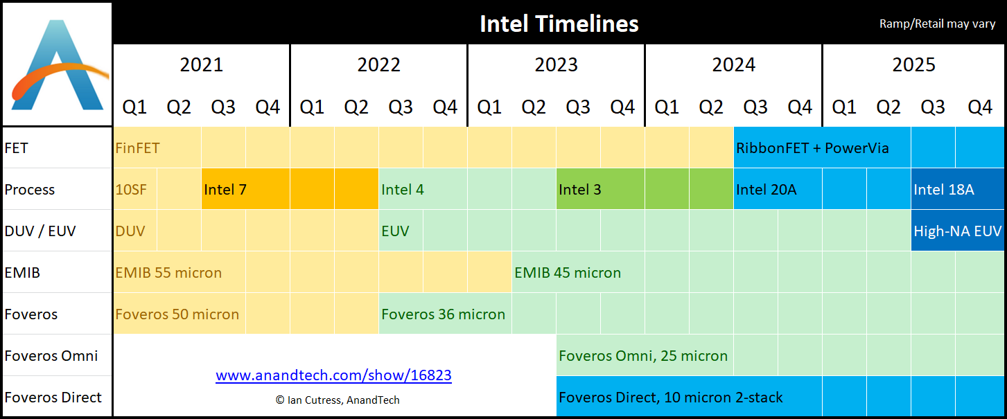
Along with Intel, the consortium also includes IBM, Cadence, Synopsys and other companies, all of whom will be providing their relevant expertise and technologies to the project. These companies will be working together on what’s a fairly forward-looking service agreement, as the DoD is looking at fab needs several years down the line.  Ultimately, the group is being tasked with establishing a semiconductor IP ecosystem around Intel’s forthcoming 18A process – the most advanced process on their development roadmap – which isn’t due to start ramping until 2025.


At this point Intel and the DoD are not announcing the value of the services agreement. There is no doubt some hedging going on, and there are multiple milestones Intel & co will need to hit between now and 2025 as part of their participating in the RAMP-C program.


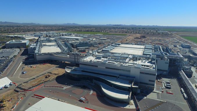
But in the meantime, even being able to claim the DoD as a major customer for Intel Foundry Services is a big win for the group, which is still in the early stages of lining up customers and proving that it has learned from past mistakes, both with regards to offering contract foundry services, and in operating a leading-edge fab ecosystem. As a reminder, Intel has previously announced that it will be spending around $20 billion to build a pair of new fabs in Arizona, so success for IFS hinges on finding big customers like the DoD to fill those fabs with orders.


Source: AnandTech – Intel Foundry Services Drafted By US Department of Defense For Next-Gen Fab Needs

Samsung Teases 512 GB DDR5-7200 Modules

This week as part of the annual Hot Chips semiconductor conference, Samsung’s memory division has presented a poster/slides on a project it is currently working on with impressive end-point results. The company details a 512 GB module of DDR5 memory, running at DDR5-7200, designed for server and enterprise use. This is a step up from the 256 GB modules at the top end of the market today, but to get there, Samsung has been introducing some new features and functionality.


Source: AnandTech – Samsung Teases 512 GB DDR5-7200 Modules

An AnandTech Interview with Jim Anderson, CEO of Lattice Semiconductor

In our coverage of the semiconductor space, we typically think of two main vectors of hardware – the CPU and the GPU. Beyond that, we look at FPGAs, microcontrollers, and this decade is bringing the advent of the dedicated AI processor. What ties all of these products together is actually the FPGA – a field programmable gate array that allows a skilled technician to essentially build a custom circuit out of configurable gates. This means an FPGA can be used to design and simulate a full CPU or GPU, but also an FPGA offers a reconfigurable way to offer optimized compute power that adapts to the needs of its users without the cost of millions or tens of millions to design dedicated silicon. One of the first FPGA companies on the market was Lattice Semiconductor, which now focuses on small power efficient FPGA designs that end up in everything from consumer devices to servers.


Over the last three years at Lattice, Jim has initiated a cultural shift that is playing out in the company roadmaps – new products, a more agile approach, and a need to focus on enabling machine learning at every part of its product stack. The recent financial disclosures at Lattice show an increasing demand for its hardware, as well as the company making strides to double its addressable market over the next five years. I thought this would be a good time to reconnect with Jim to find out exactly what he’s doing at Lattice to earmark the next generation of growth at this foundational FPGA company.


Source: AnandTech – An AnandTech Interview with Jim Anderson, CEO of Lattice Semiconductor

Intel Architecture Day 2021: Intel Unveils XeSS Image Upscaling Technology

Alongside a sneak peek at their forthcoming Xe-HPG architecture, the other big reveal today from Intel’s consumer graphics group comes from the software side of the business. Along with preparing Intel’s software stack for the 2022 launch of the first Arc products, the group has also been hard at work at their own take on modern, neural net-driven image upscaling techniques. The product of that research is Xe Super Sampling, or XeSS, which Intel is pitching as the best solution yet for high image quality and low processing cost image upscaling.


Source: AnandTech – Intel Architecture Day 2021: Intel Unveils XeSS Image Upscaling Technology

Intel Architecture Day 2021: Alder Lake, Golden Cove, and Gracemont Detailed

This week Intel held its annual Architecture Day event for select press and partners. As with previous iterations, the company disclosed details about its next generation architectures set to come to the market over the next twelve months. Intel has promised the release of its next-generation consumer and mobile processor family, Alder Lake, to come by the end of the year and today the company is sharing a good number of details about the holistic design of the chips as well as some good detail about the microarchitectures that form this hybrid design: Golden Cove and Gracemont. Here is our analysis of Intel’s disclosure.


Source: AnandTech – Intel Architecture Day 2021: Alder Lake, Golden Cove, and Gracemont Detailed

Intel Architecture Day 2021: A Sneak Peek At The Xe-HPG GPU Architecture

For Intel’s 2021 Architecture Day presentations, the yin to the CPU company’s traditional yang is GPUs. Intel has spent the last few years preparing to enter the market for discrete GPUs, with aims of competing in everything from consumer video cards up to HPC-class accelerators. And now, as the company already begins preparing for 2022, those efforts are finally coming to a head. Intel’s big breakout effort in the discrete GPU space starts in earnest next year with Xe-HPG and Xe-HPC, so for their 2021 architecture day, Intel is opening up a bit more about the GPU architectures that will be driving their first wave of high-performance products next year.


Source: AnandTech – Intel Architecture Day 2021: A Sneak Peek At The Xe-HPG GPU Architecture

MSI Launches MEG X570S Ace Max Motherboard, Max Out Ryzen 5000

On the back of a myriad of new motherboard launches based on AMD’s X570 chipset, we have the MSI MEG X570S Ace Max. The new Max motherboard supersedes the previous X570 Ace, and fittingly has lots of new and improved features. Some of the biggest features of the new Ace Max include a large 18-phase power delivery with premium 90 A power stages and the inclusion of an Intel Wi-Fi 6E wireless interface. Other features include four PCIe 4.0 x4 M.2 slots, support for DDR4-5300 memory, and 2.5 Gigabit Ethernet.


Perhaps on par with MSI’s flagship X570 model, the Godlike, the MSI MEG X570S Ace Max looks to take things to the next level with a stylish all-black design with contrasting gold stripes and multiple areas of integrated RGB lighting. Looking at PCIe support on the X570S Ace Max, it includes three full-length PCIe 4.0 slots that operate at x16 or x8/x8/+x4, with a single PCIe 4.0 x1 slot. The latter of which unfortunately shares bandwidth with the Wi-Fi 6E module, so when that is in use, the slot is disabled.


Looking at storage options, the MSI MEG X570S Ace Max has four PCIe 4.0 x4 M.2 slots, including three with support for SATA drives, as well as eight SATA ports with support for RAID 0, 1, and 10 arrays. MSI also includes an M.2 Xpander-Z Gen4 S M.2 PCIe 4.0 addon card for users looking to add more M.2 storage. Memory support is also impressive, with support for up to DDR4-5300 and a maximum supported capacity of up to 128 GB across four memory slots. Keeping the system cool is a combined total of eight 4-pin headers, including one designated to a CPU fan, one for a water pump, and six for chassis fans. MSI also has a premium power delivery, with an 18-phase design using 90 A power stages versus the 60 A power stages used on the original MEG X570 Ace.


The rear panel has a solid array of input and output befitting a premium model, including one USB 3.2 G2x2 Type-C, three USB 3.2 G2 Type-A, four USB 3.2 G1 Type-A, and four USB 2.0 ports. It uses a Realtek RTL8125B 2.5 GbE controller for Ethernet, and Intel’s latest AX210 Wi-Fi 6E wireless interface for Wi-Fi, offering access to the 6 GHz band and support for BT 5.2 devices. There’s also a premium onboard audio pairing of a Realtek ALC4082 HD audio codec and an ESS Sabre 9018Q2C DAC.


At the time of writing, we don’t have pricing information or when the MSI MEG X570S Ace Max will be available at retail, but we expect this to be within the coming months. 


Source: MSI


Related Reading


Source: AnandTech – MSI Launches MEG X570S Ace Max Motherboard, Max Out Ryzen 5000

SanDisk Extreme PRO and Crucial X6 4TB Portable SSDs Review: Contrasting High-Capacity Storage Options

The portable SSD market has been steadily expanding thanks to the increasing digital footprint of consumers. Technological advancements such as 3D NAND with high layer counts and the emergence of QLC have enabled SSD capacities to increase substantially over the last few years. And with those economies of scale kicking in, multiple vendors are finally able to offer consumer-focused flash-based storage devices in capacities up to 4TB.

At the 2021 CES, Western Digital introduced 4TB variants of almost all their portable SSD families, including their flagship SanDisk Extreme PRO v2 and the WD_BLACK P50 lines. In March, Crucial updated its affordable X6 lineup to include a 4TB version. WD’s flagships and Crucial’s mainstream X6 offerings represent two ends of the pricing spectrum. At the same capacity point, they present an interesting view of the tradeoffs involved in bringing a portable SSD to the market. Read on for an analysis of the performance and value propositions of the SanDisk Extreme PRO v2 and the Crucial X6 4TB portable SSDs.


Source: AnandTech – SanDisk Extreme PRO and Crucial X6 4TB Portable SSDs Review: Contrasting High-Capacity Storage Options

SK Hynix Releases 2TB Version of Gold P31 NVMe SSD

Coming off of the popular reception of their first family of retail NVMe SSDs, SK hynix this morning is adding another model to the Gold P31 family: the long-awaited 2TB version. The higher capacity drive, still using SK hynix’s in-house controller and 128L NAND, is being launched with immediate availability today, with retail pricing set at $280.


Source: AnandTech – SK Hynix Releases 2TB Version of Gold P31 NVMe SSD

Colorful Launches Two White Mini-ITX Motherboards For Intel Rocket Lake

Colorful has unveiled two new motherboards designed for Intel Rocket Lake and Comet Lake processors. The CVN B560I Gaming V20 and CVN B560I Gaming Frozen are based on the Mini-ITX form factor, and both share the same feature set; the only difference is in the aesthetics. The most prominent features include one PCIe 4.0 x4 M.2 slot, four SATA ports, and a Gigabit Ethernet controller.


Designed around the budget-friendly Intel B560 chipset for 11th and 10th generation Intel desktop processors, both the Colorful CVN B560I Gaming V20 and Frozen models include an unspecified 8-phase power delivery (6+2), with one 8-pin 12 V ATX CPU power input and a 24-pin 12 V ATX motherboard inputs. On the right-hand side of the board are a pair of memory slots with support for up to DDR4-4266 and can accommodate up to 64 GB. 


At the time of writing, Colorful hasn’t divulged its controller set, but we know it has one PCIe 4.0 x4 M.2 slot and one full-length PCIe 4.0 x16 slot along the bottom of the board. For cooling, both boards include three 4-pin fan headers with four straight-angled SATA ports, which can be found on the right-hand side of the PCB. The only difference between both models is that the Frozen variant has a white PCB, and the V20 uses a black PCB. This gives users the option to find a solution to fit their systems aesthetic; However, Colorful doesn’t specify if either model includes integrated RGB LED lighting. We would assume neither does based on the images.


Both models share the same rear panel I/O layout and include one USB 3.2 G2 Type-C, two USB 3.2 G2 Type-A, and two USB 2.0 ports. Colorful provides a pair of video outputs, including HDMI and DisplayPort, while an unspecified HD audio codec powers three 3.5 mm audio jacks. Regarding networking, there’s one Gigabit Ethernet port and a Wi-Fi 6 CNVi, which also includes support for BT 5.0 devices. 


At present, Colorful hasn’t provided pricing or when the CVN B560I Gaming V20 and Gaming Frozen models will hit retail shelves.


Source: Colorful


Related Reading


Source: AnandTech – Colorful Launches Two White Mini-ITX Motherboards For Intel Rocket Lake

ASUS Unveils N5105I-IM-A, Intel Jasper Lake in Mini-ITX Form

Back in January, Intel launched its Jasper Lake platform with a range of dual-core and quad-core Tremont Atom-based processors.. Primarily aimed at the notebook and Chromebook market, Intel’s Jasper Lake Celeron and Pentium Silver chips are using 10nm Tremont Atom cores as low as 6 W. Today we have learned that ASUS has unveiled its first Jasper Lake system via the N5105I-IM-A mini-ITX motherboard for the DIY market, with a passively cooled design, and supports the Intel Celeron N5105 4-core 4-thread processor.


Based on the small form factor mini-ITX platform, the ASUS N5105I-IM-A includes two SO-DIMM memory slots, although ASUS hasn’t revealed a full list of the specifications. It is using a 4-pin 12 V ATX power input, with an additional 4-pin 12 V power output. The N5105I-IM-A is designed to support Intel’s Celeron N5105 processor, which features four Tremont Atom cores, four threads, and features a base frequency of 2 GHz, a turbo frequency of 2.9 GHz, and has a 10 W TDP. 


Due to the low power by the Intel Celeron N5105, ASUS has opted for a gold-colored copper CPU heatsink, which comes supplied with the board. Looking at onboard connectivity, ASUS includes what looks like a single PCIe 3.0 x1 slot, with two SATA ports and one 4-pin fan header for a chassis fan. Video is provided by the graphics on the CPU.


On the rear panel is a range of input and output, including two video outputs consisting of an HDMI and D-sub output, with three Serial ports. The board also includes support for an RJ11/DIO connector that is regularly used for cash registers and an MSR/RFID reader for credit and debit card payments. In terms of USB, four Type-A ports are likely USB 3.0, and it also includes one Ethernet port that an unspecified controller powers. 


At the time of writing, we don’t have any information on the pricing or the availability of the ASUS N5105I-IM-A motherboard.


Source: FanlessTech


Related Reading


Source: AnandTech – ASUS Unveils N5105I-IM-A, Intel Jasper Lake in Mini-ITX Form

The "Smartphone for Snapdragon Insiders" vs ROG5 Preview: Branded vs Original

Today we’re reviewing a rather unusual device, the new ASUS “Smartphone for Snapdragon Insiders”. The device had been first announced a month ago by Qualcomm and ASUS, and represents a sort of weird kind of collaboration between the two companies. 


Source: AnandTech – The “Smartphone for Snapdragon Insiders” vs ROG5 Preview: Branded vs Original

Intel Video Cards Get a Brand Name: Arc, Starting with "Alchemist" in Q1 2022

After several months of various teasers, Intel is finally starting to put the band together for their first high-performance discrete GPUs and video cards. This morning the company is kicking its pre-launch marketing game into high gear by announcing a new brand name that these video cards will sold under: Arc. As well, the company is finally giving us our first real (albeit wide) launch window for the hardware. The first Arc video cards, based on the “Alchemist” generation of hardware, will be released in the first quarter of 2022, kicking off Intel’s formal foray into high-performance discrete consumer graphics for desktop and mobile.


Source: AnandTech – Intel Video Cards Get a Brand Name: Arc, Starting with “Alchemist” in Q1 2022