Apple Announces M1 Pro & M1 Max: Giant New Arm SoCs with All-Out Performance

Today’s Apple Mac keynote has been very eventful, with the company announcing a new line-up of MacBook Pro devices, powered by two different new SoCs in Apple’s Silicon line-up: the new M1 Pro and the M1 Max.


The M1 Pro and Max both follow-up on last year’s M1, Apple’s first generation Mac silicon that ushered in the beginning of Apple’s journey to replace x86 based chips with their own in-house designs. The M1 had been widely successful for Apple, showcasing fantastic performance at never-before-seen power efficiency in the laptop market. Although the M1 was fast, it was still a somewhat smaller SoC – still powering devices such as the iPad Pro line-up, and a corresponding lower TDP, naturally still losing out to larger more power-hungry chips from the competition.


Today’s two new chips look to change that situation, with Apple going all-out for performance, with more CPU cores, more GPU cores, much more silicon investment, and Apple now also increasing their power budget far past anything they’ve ever done in the smartphone or tablet space.


Source: AnandTech – Apple Announces M1 Pro & M1 Max: Giant New Arm SoCs with All-Out Performance

The Apple 2021 Fall Mac Event Live Blog 10am PT (17:00 UTC)

Following last month’s announcement event of Apple’s newest iPhone and iPad line-ups, today we’re seeing Apple hold its second fall event, where we expect the company to talk about all new things Mac. Last year’s event was a historic one, with Apple introducing the M1 chip and new powered Mac devices, marking the company’s move away from x86 chips from Intel, taking instead their own future in their hands with their own custom Arm silicon. This year, we’re expecting more chips and more devices, with even more performance to be release. Stay tuned as we cover tonight’s show.


Source: AnandTech – The Apple 2021 Fall Mac Event Live Blog 10am PT (17:00 UTC)

TSMC Roadmap Update: 3nm in Q1 2023, 3nm Enhanced in 2024, 2nm in 2025

TSMC has introduced a brand-new manufacturing technology roughly every two years over the past decade. Yet as the complexity of developing new fabrication processes is compounding, it is getting increasingly difficult to maintain such a cadence. The company has previously acknowledged that it will start producing chips using its N3 (3 nm) node about four months later than the industry is used to (i.e., Q2), and in a recent conference call with analysts, TSMC revealed additional details about its latest process technology roadmap, focusing on their N3, N3E, and N2 (2 nm) technologies.


N3 in 2023


TSMC’s N3 technology will provide full node scaling compared to N5, so its adopters will get all performance (10% – 15%), power (-25% ~ -30%), and area (1.7x higher for logic) enhancements that they come to expect from a new node in this day and age. But these advantages will come at a cost. The fabrication process will rely extensively on extreme ultraviolet (EUV) lithography, and while the exact number of EUV layers is unknown, it will be a greater number of layers than the 14 used in N5. The extreme complexity of the technology will further add to the number of process steps – bringing it toto well over 1000 – which will further increase cycle times. 


As a result, while mass production of the first chips using TSMC’s N3 node will begin in the second half of 2022, the company will only be shipping them to an undisclosed client for revenue in the first quarter of 2023. Many observers, however, expected these chips to ship in late 2022.


“N3 risk production is scheduled in 2021, and production will start in second half of 2022,” said C.C. Wei, CEO of TSMC. “So second half of 2022 will be our mass production, but you can expect that revenue will be seen in first quarter of 2023 because it takes long — it takes cycle time to have all those wafer out.”


N3E in 2024


Traditionally, TSMC offers performance-enhanced and application-specific process technologies based on its leading-edge nodes several quarters after their introduction. With N3, the company will be changing their tactics somewhat, and will introduce a node called N3E, which can be considered as an enhanced version of N3. 


This process node will introduce an improved process window with performance, power, and yield enhancements. It is unclear whether N3 meets TSMC’s expectations for PPA and yield, but the very fact that the foundry is talking about improving yields indicates that there is a way to improve it beyond traditional yield boosting methods. 


“We also introduced N3E as an extension of our N3 family,” said Wei. “N3E will feature improved manufacturing process window with better performance, power and yield. Volume production of N3E is scheduled for one year after N3.”


TSMC has not commented on whether N3E will be compatible with N3’s design rules, design infrastructure, and IPs. Meanwhile, since N3E will serve customers a year after N3 (i.e., in 2024), there will be quite some time for chip designers to prepare for the new node.


N2 in 2025


TSMC’s N2 fabrication process has largely been a mystery so far. The company has confirmed that it was considering gate-all-around field-effect transistors (GAAFETs) for this node, but has never said that the decision was final. Furthermore, it has never previously disclosed a schedule for N2. 


But as N2 gets closer, TSMC is slowly locking down some additional details. Particularly, the company is now formally confirming that the N2 node is scheduled for 2025. Though they are not elaborating on whether this means HVM in 2025, or shipments in 2025.


“I can share with you that in our 2-nm technology, the density and performance, will be the most competitive in 2025,” said Wei.


Source: AnandTech – TSMC Roadmap Update: 3nm in Q1 2023, 3nm Enhanced in 2024, 2nm in 2025

TSMC to Build Japan's Most Advanced Semiconductor Fab

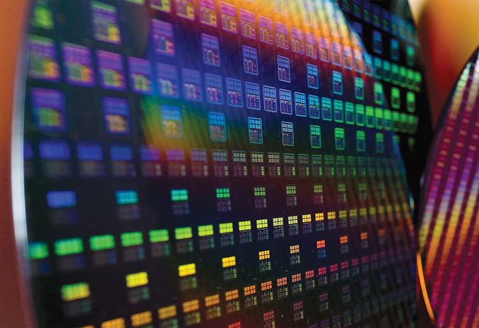
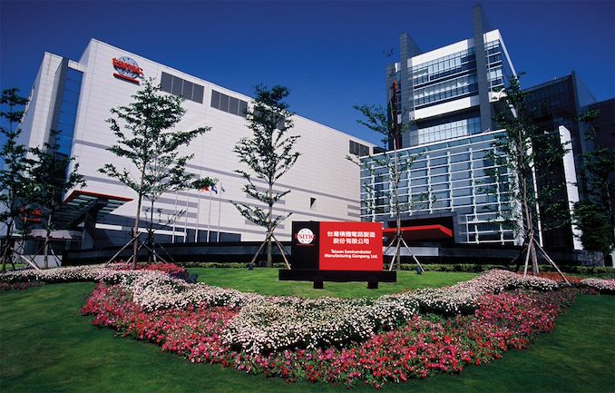
Fabs are well-known for being an expensive business to be in, so any time a new fab is slated for construction, it tends to be a big deal – especially amidst the current chip crunch. To that end, TSMC this week has announced plans to build a new, semi-specialized fab in Japan to meet the needs of its local customers. The semiconductor manufacturing facility will focus on mature and specialty fabrication technologies that are used to make chips with long lifecycles for automakers and consumer electronics. The fab will be Japan’s most advanced fab for logic when it becomes operational in late 2024 and if the rumors about planned investments are correct, it could also be Japan’s largest fab for logic chips.


“After conducting due diligence, we announce our intention to build a specialty technology fab in Japan, subject to our board of directors approval,” announced CC Wei, chief executive officer of TSMC, during a conference call with investors and financial analysts. “We have received a strong commitment to support this project from both our customers and the Japanese government.”


Comes Online in Late 2024


TSMC’s fab in Japan will process 300-mm wafers using a variety of specialty and mature nodes, including a number of 28 nm technologies as well as 22ULP process for ultra-low-power devices. These nodes are not used to make leading-edge ASICs and SoCs, but they are widely used by automotive and consumer electronics industries and will continue to be used for years to come not only for existing chips, but for upcoming solutions as well. 


“This fab will utilize 20 nm to 28 nm technology for semiconductor wafer fabrication,” Wei added. “Fab construction is scheduled to begin in 2022 and production is targeted to begin in late 2024, further details will be provided subject to the board approval.”


While TSMC disclosed the specialized nature of the fab, its schedule, and the fact that it gained support from clients and the Japanese government, the company is not revealing anything beyond that. In fact, while it confirmed that the cost of the semiconductor production facility is not included in its $100 billion three-year CapEx plan, it refused to give any estimates about its planned investments in the project.


Meanwhile, there are many things that make this fab special for TSMC, Japan, and the industry.


The Most Advanced Logic Fab in Japan


It was late 2005, AMD and Intel started to ship their first dual-core processors and the CPU frequency battle was officially over. Intel was getting ready to introduce its first 65nm chips in early 2006 and all of a sudden Panasonic said that it had started volume production of the world’s first application processors using a 65 nm technology, which it co-developed with Renesas, putting Panasonic a couple of months ahead of mighty Intel. In mid-2007, Panasonic again beat Intel to punch by several months with its 45 nm fabrication process.


But with their 32 nm node, Panasonic was 9 – 10 months behind Intel. And while the company did a half-node shrink of this process, it ultimately pulled the plug on 22nm following other Japanese conglomerates that opted out from the process technology race even earlier. By now, all Japanese automotive and electronics companies outsource their advanced chips to foundries, who in turn, build the majority of them outside of Japan.


By bringing a 22ULP/28nm-capable fab to Japan, TSMC’s plans will not only brings advanced logic manufacturing back to the country, but it would also amount to the most advanced fab in Japan. TSMC is also constructing an R&D center in Japan and cooperates with the University of Tokyo on various matters, so its presence in the country is growing, which is good news for the local semiconductor industry.


Previously TSMC concentrated its fabs and R&D facilities in Taiwan, but it looks like its rapid growth fueled by surging demand for semiconductors as well as geopolitical matters are compelling the foundry to diversify its production and R&D locations. 


What is particularly interesting is that according to a Nikkei report, the Japanese production facility will be co-funded by TSMC, the Japanese government, and Sony. This marks another major strategy shift for TSMC, which tends to fully own its fabs. In fact, if the Nikkei report is to be believed, the whole project will cost around $7 billion (though it is not said whether this is the cost of first phase of the fab, or a potential multi-year investment).


To put the number into context, SMIC recently announced plans to spend around $8.87 billion on a fab with planned capacity of around 100,000 300-mm wafer starts per month (WSPM). TSMC’s facility will presumably cost less and will be built in a country with higher operating costs, so it may well not be a GigaFab-level facility (which have capacity of ~100K WSPM). But still, we are talking about a sizable fab that could have a capacity of tens of thousands of wafer starts per month, which would make it Japan’s biggest 300-mm logic facility ever. Just for comparison, the former Panasonic fab in Uozo (now controlled by Tower Semiconductor and Nuvoton) has a capacity of around 8,000 WSPM.


TSMC has not formally confirmed any numbers about its Japanese fab, but the company tends to build rather large production facilities that can be expanded if needed. Meanwhile, a fab in Japan that well serve needs of local automotive and electronics conglomerates promises to help them to avoid shortages of chips in the future. This would also leave TSMC free to assign its 28nmTaiwanese and Chinese production lines to other applications, including PCs, which is important for the whole industry.


Source: AnandTech – TSMC to Build Japan’s Most Advanced Semiconductor Fab

G.Skill Unveils Premium Trident Z5 and Z5 RGB DDR5 Memory, Up To DDR5-6400 CL36

With memory manufacturers clamoring over themselves to push out DDR5 in time for the upcoming launch of Intel’s Alder Lake processors, G.Skill has unveiled its latest premium Trident Z5 kits. The latest Trident kits are based on Samsung’s new DDR5 memory chips and range in speed from DDR5-5600 to DDR5-6400, with latencies of either CL36 or CL40. Meanwhile, G.Skill has also opted to use this opportunity to undertake a complete design overhaul from its previous DDR4 memory, with a fresh new look and plenty of integrated RGB, and is .


G.Skill Trident Z5 DDR5 Memory Specifications
Speed Latencies Voltage Capacity
DDR5-6400 36-36-36-76

40-40-40-76
??? 32 GB (2 x 16 GB)
DDR5-6000 36-36-36-76

40-40-40-76
??? 32 GB (2 x 16 GB)
DDR5-5600 36-36-36-76

40-40-40-76
??? 32 GB (2 x 16 GB)


Looking at performance, the top SKU comes with fast speeds of DDR5-6400, with either a latency of CL 36-36-36-76 or CL 40-40-40-76. Both the lower-rated kits of DDR5-6000 and DDR5-5600 are available with the same latencies, while all of the six combinations will be available in 32 GB kits, with 2 x 16 GB memory modules. The new G.Skill Trident Z5 and Z5 RGB memory kits will also feature the latest Samsung memory ICs, with G.Skill hand screening the memory chips themselves to ensure maximum stability and performance.


At the time of writing, G.Skill hasn’t confirmed the operating voltages of each kit. G.Skill also hasn’t unveiled its pricing at this time, but it did say that the Trident Z5 and Trident Z5 RGB kits will be available from November.


Meanwhile in terms of aesthetics, the G.Skill Trident Z5 DDR5 memory features a new design compared with previous Trident Z series kits. The Trident Z5 comes with a new dual texture heat spreader design and is available either with a black top bar (Z5) or a new translucent RGB light bar (Z5 RGB). It’s also available in black and silver, with a black brushed aluminum insert across both colors, making it stand out.


With the RGB enabled G.Skill Trident Z5 RGB DDR5 memory kits, the lighting can be customized via its Trident Z lighting control software or synced with other third-party software supplied by vendors such as ASRock, ASUS, GIGABYTE, and MSI’s own RGB software.


Gallery: G.Skill


Related Reading


Source: AnandTech – G.Skill Unveils Premium Trident Z5 and Z5 RGB DDR5 Memory, Up To DDR5-6400 CL36

The EVGA Z590 Dark Motherboard Review: For Extreme Enthusiasts

Getting the most out of Intel’s Core i9-11900K primarily relies on two main factors: premium cooling for the chip itself, and a solid motherboard acting as the foundation. And while motherboard manufacturers such as EVGA can’t do anything about the former, they have quite a bit of experience with the latter.

Today we’re taking a look at EVGA’s Z590 Dark motherboard, which is putting EVGA’s experience to the test as one of a small handful of LGA1200 motherboards geared for extreme overclocking. A niche market within a niche market, few people really have the need (or the means) to overclock a processor within an inch of its life. But for those that do, EVGA has developed a well-earned reputation with its Dark series boards for pulling out all of the stops in helping overclockers get the most out of their chips. And even for the rest of us who will never see a Rocket Lake chip pass 6GHz, it’s interesting to see just what it takes with regards to motherboard design and construction to get the job done.


Source: AnandTech – The EVGA Z590 Dark Motherboard Review: For Extreme Enthusiasts

The Be Quiet! Pure Loop 280mm AIO Cooler Review: Quiet Without Compromise

Today we’re taking our first look at German manufacturer Be Quiet’s all-in-one (AIO) CPU liquid coolers, with a review of their Pure Loop 280mm cooler. True to their design ethos, Be Quiet! has built the Pure Loop to operate with as little noise as is reasonably possible, making for a record-quiet cooler that also hits a great balance between overall performance, an elegant appearance, and price.


Source: AnandTech – The Be Quiet! Pure Loop 280mm AIO Cooler Review: Quiet Without Compromise

AMD Launches Radeon RX 6600: More Mainstream Gaming For $329

AMD this morning is once again expanding its Radeon RX 6000 family of video cards, this time with the addition of a second, cheaper mainstream offering: the Radeon RX 6600. Being announced and launched this morning, the Radeon RX 6600 is aimed at the mainstream 1080p gaming market, taking its place as a second, cheaper alternative to AMD’s already-released Radeon RX 6600 XT. Based on the same Navi 23 GPU as its sibling, the Radeon RX 6600 comes with 28 CUs’ worth of graphics hardware, 8GB of GDDR6 VRAM, and a 32MB Infinity Cache, with prices starting at $329.


Source: AnandTech – AMD Launches Radeon RX 6600: More Mainstream Gaming For 9

Netgear Updates Orbi Lineup with RBKE960 Wi-Fi 6E Quad-Band Mesh System

Mesh networking kits / Wi-Fi systems have become quite popular over the last few years. Despite competition from startups such as eero (now part of Amazon) and Plume (with forced subscriptions), as well as big companies like Google (Google Wi-Fi and Nest Wi-Fi), Netgear’s Orbi continues to enjoy popularity in the market. Orbi’s use of a dedicated backhaul provides tangible benefit over other Wi-Fi systems using shared backhauls. However, the costs associated with the additional radio have meant that the Orbi Wi-Fi systems have always carried a premium compared to the average market offerings in the space.


Netgear introduced their first Wi-Fi 6E router – the Nighthawk RAXE500 – at the 2021 CES. Priced at $600, the router utilized a Broadcom platform (BCM4908 network processing SoC + BCM46384 4-stream 802.11an/ac/ax radio). Today, the company is updating the Orbi lineup with a Wi-Fi 6E offering belonging to the AXE11000 class. Based on Qualcomm’s Hawkeye (IPQ8074) / Pine (QCN9074) platform, the company is touting their RBKE960 Orbi series to be the world’s first quad-band Wi-Fi 6E mesh system.


Netgear’s high-end Orbi kits have traditionally been tri-band solutions, with a second 5 GHz channel as a dedicated backhaul. With Wi-Fi 6E, a tri-band solution is mandated – 2.4 GHz, 5 GHz, and 6 GHz support are all needed for certification. The 6 GHz channel, as discussed previously, opens up multiple 160 MHz channels that are free of interference. The RBKE960 series supports the three mandated bands, and also retains a dedicated 5 GHz backhaul, making it a quad-band solution with combined Wi-Fi speeds of up to 10.8 Gbps across all four considered together.


Netgear has opted to retain 5 GHz for the backhaul in order to maximize range. While the 6 GHz band is interference-free, the power restrictions prevent the communication in those channels from having as much range as the existing 5 GHz ones. Having a dedicated backhaul ensures that all the ‘fronthaul’ channels are available for client devices (shared backhauls result in a 50% reduction in speeds available for client devices for each additional node / satellite). The benefits of Wi-Fi 6E and what consumers can expect from the 6GHz band have already been covered in detail in our Nighthawk RAXE500 launch piece. The Orbi RBKE960 series supports up to seven 160 MHz channels, allowing for interference-free operation even in dense apartments with multiple neighbors.


The RBKE960 supports 16 Wi-Fi streams, making for an extremely complex antenna design. Netgear has made improvements based on past experience to the extent that the new Orbi RBKE960 performs better than the Orbi RBK850 even for 5GHz communication (the larger size of the unit also plays a part in this).


In terms of hardware features, the router sports a 10G WAN port, 3x 1GbE, and 1x 2.5GBASE-T ports. The satellite doesn’t have the WAN port, but retains the other three. The 2.5GBASE-T port can be used to create an Ethernet backhaul between the router and the satellite. On the software side, the new Orbi creates four separate Wi-Fi networks for different use-cases.


The reduced range in the 6GHz band means that large homes might require multiple satellites to blanket the whole area with 6GHz coverage.


Installation and management is via the Orbi app. Netgear also includes the NETGEAR Armor cyber-security suite with integrated parental controls – some features in Armor are subscription-based.


Netgear is also introducing an ‘Orbi Black Edition’ available exclusively on Netgear’s own website. With the RAXE500 setting the stage with its $600 price point, it is no surprise that the RBSE960 satellite costs the same (trading the WAN port and other features for an extra 4×4 radio). A kit with a router and a single satellite (RBKE962) is priced at $1100, while the RBKE963 (an additional satellite) bumps up the price tag to $1500. With home Wi-Fi becoming indispensable thanks to the work-from-home trend among other things, Netgear believes consumers will be ready to fork out what is essentially the price of a high-end smartphone or notebook for a reliable and future-proof Wi-Fi solution.


Source: AnandTech – Netgear Updates Orbi Lineup with RBKE960 Wi-Fi 6E Quad-Band Mesh System

SanDisk Professional G-DRIVE SSD and ArmorLock SSD Review

Western Digital introduced the SanDisk Professional branding in May 2021 for its G-Technology products targeting the content-capture market. The company has taken the opportunity to update some of the hardware in the process of transitioning from G-Technology to the new branding. The G-DRIVE family represents the lineup of single-disk direct-attached storage units from SanDisk Professional. Today’s review takes a look at the G-DRIVE SSD and G-DRIVE ArmorLock SSD – two bus-powered portable SSDs with a USB 3.2 Gen 2 interface that target very different use-cases.


Source: AnandTech – SanDisk Professional G-DRIVE SSD and ArmorLock SSD Review

Apple's iPhone 13 Series Screen Power, Battery Life Report – Long Lasting Devices

Following our last week’s preview into the new iPhone 13 series’ A15 chip, which impressed us tremendously due to its efficiency gains, we promised next to have a closer look at the new phone’s battery life and how the new display generation and screen efficiency ties in with the SoC efficiency and increased battery capacities this generation.


Source: AnandTech – Apple’s iPhone 13 Series Screen Power, Battery Life Report – Long Lasting Devices

The EVGA X570 Dark Motherboard Review: A Dark Beast For Ryzen

Quite a few of the motherboards we have reviewed over the last month have been aimed at enthusiasts with a penchant for extreme overclocking. Today’s review focuses on the EVGA X570 Dark that is more than the usual desktop AM4 motherboard. It’s EVGA’s first entry into the market for AMD’s Ryzen processors, focusing on performance and overclocking more than most other X570/X570S boards currently available. Some of the EVGA X570 Dark’s most notable features include two memory slots with support for DDR4-4800, dual PCIe 4.0 x4 M.2, eight SATA, dual 2.5 GbE, and support for Wi-Fi 6. Is EVGA, which had previously been an Intel and NVIDIA only deal until now, enough to tempt you to the ‘DARK’ side? Time to take a look and see if the X570 Dark has enough about it to justify the combination of an unconventional design and premium price tag.


Source: AnandTech – The EVGA X570 Dark Motherboard Review: A Dark Beast For Ryzen

Seagate Updates Game Drive SSD for Xbox with New Look and Internals

Seagate has been maintaining a line of Xbox-certified external SSDs since late 2016. The current Game Drive for Xbox SSD is based on the Seagate Fast SSD’s internals and industrial design. With the USB 3.2 Gen 1 (BarraCuda) Fast SSD reaching EOL (that market segment has since moved on to USB 3.2 Gen 2), the time has now come for Seagate to revamp the internals of the Game Drive for Xbox SSD and give it a new look.


The company is introducing a new Game Drive for Xbox SSD that takes inspiration from the currently available HDD equivalent – sporting a sleek all-black look with a green LED bar. The 96mm x 50mm x 11mm bus-powered portable SSD weighs just 51g, and sports a USB 3.2 Gen 1 micro-Binterface. It is compatible with Xbox Series X, Series S, and all generations of Xbox One. The package includes a 46cm USB 3.0 cable (micro-B to Type-A).


Seagate is planning to launch only a single SKU of the new product – a 1TB version (STLD1000400) for $170. Interestingly, the 3-year warranty is also accompanied by data-loss protection using Seagate’s Rescue Data Recovery Services. Availability is slated for later this month, well in time for the holiday season.


The article will be updated with additional information once we hear back from Seagate regarding details of the SSD’s internals.


Source: AnandTech – Seagate Updates Game Drive SSD for Xbox with New Look and Internals

Samsung Foundry: 2nm Silicon in 2025

One of the key semiconductor technologies beyond 3D FinFET transistors are Gate-All-Around transistors, which show promise to help extend the ability to drive processors and components to higher performance and lower power. Samsung has always announced that its first generation GAA technology will align with its ‘3nm’ nodes, with its 3GAE and 3GAP processes. As part of the Samsung Foundry Forum today, some more insight was put into the timeline for the rollout, as well as talk of its 2nm process.


Source: AnandTech – Samsung Foundry: 2nm Silicon in 2025

Samsung Foundry’s New 17nm Node: 17LPV brings FinFET to 28nm

Despite most discussion about chip manufacturing focusing on the leading edge and blazingly fast and complex side of the industry, the demand for the ‘legacy’ process technologies is also higher than ever, but also by volume a lot bigger than the latest and greatest. These legacy processes form the backbone of most modern electronics, and so being able to offer equivalent technology at lower cost/power is often a win-win for manufacturers and chip designers alike. To that end, Samsung is announcing a new 17nm process node, designed for customers still using a planar 28nm process, but want to take advantage of 14nm FinFET technology.


Source: AnandTech – Samsung Foundry’s New 17nm Node: 17LPV brings FinFET to 28nm

Samsung Foundry to Almost Double Output by 2026

It’s hard not to notice that we’re in the middle of a semiconductor crunch right now. Factories are running at full steam, but pinch points in the supply chain are causing chaos and bottlenecks – whether that means not enough packaging materials, the cost of shipping has increased 10x, or additional tariffs, it’s causing various industries that rely on semiconductors to wait for supply and then pay over expected prices. Nonetheless, everything that is made is being sold, and so all of the big foundries are driving more investment into their supply chain ecosystem as well as raw manufacturing, and Samsung is no different.


Source: AnandTech – Samsung Foundry to Almost Double Output by 2026

The Microsoft Surface Laptop Studio Review: Dynamic Design

Microsoft’s Surface team has produced some amazing designs over the years, taking to focusing on convertible devices to highlight the adaptability of Windows. That being said, over the last several years the design team has been largely held in check, as Microsoft has opted to focus on further refining their convertible designs. Thankfully, for 2021 the team is back to innovation as well as refinement with their latest device, the Surface Laptop Studio. With its dynamic woven hinge, the Laptop Studio is a true convertible device, as well as the spiritual successor to the now-defunct Surface Book.


Source: AnandTech – The Microsoft Surface Laptop Studio Review: Dynamic Design

What to Expect with Windows 11: A Day One Hands-On

Tomorrow, Microsoft is officially launching Windows 11, the next installment of their operating system which underpins the majority of PCs in use today. Windows 10 has an install base of over 1 billion devices, and Windows 11 comes into existence in a much different place than its predecessor. After the much-maligned Windows 8 there was a sense of urgency and necessity which ushered Windows 10 into the world. Windows 11, on the other hand, comes into a market where most people are happy with Windows 10. So it raises the question: Why now?


Source: AnandTech – What to Expect with Windows 11: A Day One Hands-On

ASUS GeForce RTX 3070 Noctua Edition Announced

One thing Noctua is famed for, other than its high-end design and engineering team delivering top quality air-cooling products, is the brown/beige color scheme. Some users may detest the off-key and non-conventional color, which rarely goes with other colors inside their PC, and so they have to shun Noctua and look elsewhere. Others swear by the design, and ASUS has gone one step further by teaming up with Noctua to create an NVIDIA GeForce RTX 3070 graphics card. The ASUS GeForce RTX 3070 Noctua Edition features two NF-A12x25 PWM cooling fans with a semi-passive design and aims to be one of the coolest and quietest air-cooled RTX 3070 on the market.


ASUS x Noctua: The Start of Something Bigger?


In August, Twitter user @KOMACHI_ENSAKA spotted that an ASUS and Noctua collaboration may have been in the works via a listing on the Eurasian Economic Commission (EEC) website. Putting the rumors to rest, ASUS and Noctua have announced their collaboration today, and they both present the ASUS GeForce RTX 3070 Noctua Edition, with a slightly higher clocked OC version too.


The most striking thing visually with the ASUS GeForce RTX 3070 Noctua Edition models is the dual beige Noctua NF-A12x25 PWM cooling fans attached to a custom heatsink design with multiple fins and heat pipes behind the beige. Noctua and ASUS have opted for an extensive cooling design as the RTX 3070 Noctua Edition and OC version take up 4.3 slots worth of space and measure in at 12.2 inches in length.


Both the regular and OC models operate with a semi-passive design which means that whenever the temperature drops below 50°C, the fans will switch off. Both models have a standard I/O, including dual HDMI 2.1 and three DisplayPort 1.4a video outputs. Providing power to the graphics cards is a pair of 8-pin PCIe power inputs and comes with a recommendation that users install a 750 W power supply or greater.


The ASUS GeForce RTX 3070 Noctua Edition with a dual-branded backplate


Touching on the specifications of the base model, it features a GPU base frequency of 1500 MHz, with a gaming mode boost clock of 1725 MHz and an OC mode boost clock of 1755 MHz. The OC variant features the same base clock of 1500 MHz but with more aggressive boost clocks of 1815 MHz in gaming mode and 1845 MHz in OC mode. Both models share a memory speed of 14 Gbps effective, with 5888 CUDA cores on a 256-bit memory interface and 8 GB of GDDR6 video memory. 


The ASUS GeForce RTX 3070 Noctua and OC version will be available from mid-October, although no pricing has been given at the time of writing.


Source: Noctua


Related Reading


Source: AnandTech – ASUS GeForce RTX 3070 Noctua Edition Announced