Intel Alder Lake-H Core i9-12900HK Review: MSI's Raider GE76 Goes Hybrid

At CES this year, Intel officially announced its expanded Alder Lake lineup including the performance-laptop focused H-Series processors, which traditionally fit in the 45-Watt range. Today we finally get to take a look at the 12th generation H-Series processors, the first mobile incarnation of Alder Lake, and see how Intel’s fastest mobile platform stacks up to not only Intel’s previous 11th generation Tiger Lake platform, but also AMD’s Ryzen 5000 series.


Source: AnandTech – Intel Alder Lake-H Core i9-12900HK Review: MSI’s Raider GE76 Goes Hybrid

Interview with Intel’s Dan Ragland, Head of Overclocking: Tuning Alder Lake For Performance

The topic of overclocking has been an interesting one to track over the years. Over a decade ago, when dealing with 2-4 core processors, an effective overclock gave a substantial performance uplift, often allowing a $200 processor to perform like the one that cost $999. However, core counts have increased over the last couple of years, but also companies like Intel are getting better at understanding their silicon, and are able to ship it out of the box almost at the silicon limit anyway. So what use is overclocking? We turned to Dan Ragland, who runs Intel’s Overclocking Lab in Hillsboro, Oregon, to find out what overclocking now means for Intel, what it means for Alder Lake, but also how Intel is going to approach overclocking in the future.


Source: AnandTech – Interview with Intel’s Dan Ragland, Head of Overclocking: Tuning Alder Lake For Performance

Intel Announces Ohio Fab Complex: 2 New Fabs For $20B, And Space For More

With fab expansions on tap across the entire semiconductor industry, Intel today is laying out their own plans for significantly increasing their production capacity by announcing their intention to build a new $20 billion fab complex in Ohio. With the paperwork already inked and construction set to begin in late 2022, Intel will be building two new leading-edge fabs in their new Ohio location to support future chip needs. And should further demand call for it, the Ohio complex has space to house several more fabs.


Intel’s announcement follows ongoing concerns about chip fab capacity and national security, as like other chip fabs, Intel is looking to expand their capacity in future years amidst the current chip crunch. All the while, the United States government has become increasingly mindful about how much chip production takes place in geopolitically tricky Taiwan, placing additional pressure on firms to build additional fabs within the US. To that end, Intel has been not-so-secretly undertaking a search to find a good location for a new fab campus, and they have finally found their answer in Ohio.


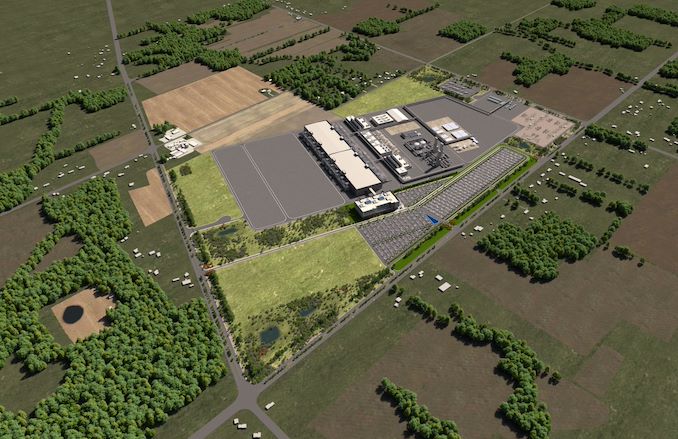
The new site, Intel’s first new manufacturing site location in 40 years, is located in New Albany, Ohio, just outside of Columbus. Up until now, all of Intel’s major chip fab sites have been in the western United States – Oregon, Arizona, and at one point, Silicon Valley – so the Ohio site is a significant move for the company. All told, the Ohio “mega-site”, as Intel likes to call it, covers nearly 1000 acres. And while Intel is only initially planning for two fabs, the site offers plenty of room to grow, offering enough space for a total of 8 fabs.


The immediate goal of the company – and the crux of today’s announcement – revolves around the building of two new leading-edge fabs at the Ohio location. According to Intel, these two fabs will begin construction late this year, with production coming online in 2025. The company isn’t formally stating what the initial process node will be – instead saying that it will be using the “industry’s most advanced transistor technologies” – however if the company is indeed building truly bleeding-edge fabs, then 2025 lines up with Intel’s 18A process, which will be 4 generations newer than what Intel is using now (Intel 7).


Altogether, Intel expects the project to cost about $20 billion, which is similar to what Intel will be spending for its two new Arizona fabs, which were announced just under a year ago. And further down the line, should Intel opt to fill the rest of the property with the other 6 fabs that the site can support, the company expects that the total price tag could reach nearly $100 billion. Ultimately, the company is making it clear that they are priming the site not just to met their mid-term production needs with the initial two fabs, but are making sure to have the space ready for further capacity expansion over the long-term.


As to whether Intel eventually builds those further 6 fabs, that will depend on a few factors. Key among these will be demand from Intel Foundry Services clients; while Intel will be using some of the Ohio site’s capacity for their own needs, the site will also be used to fab chips for IFS customers. If Intel’s bid to break into the contract fab business is successful, and the company is able to woo over additional clients/orders, then they will need to build additional fabs to meet that demand.


Also hanging in the balance is what the US Government opts for, both in terms of orders and incentives. The Ohio fabs will be used for domestic production of sensitive chips, as the US looks to secure its supply lines. Meanwhile the CHIPS for America Act and its 53 billion in incentives will also be a. Intel for its part isn’t playing coy about its interest in the CHIPS money, explicitly stating that “The scope and pace of Intel’s expansion in Ohio, however, will depend heavily on funding from the CHIPS Act”. In some respects Intel is taking a bit of a gamble by investing in the Ohio location before any CHIPS funding is approved – on a pure cost basis, overseas production is traditionally cheaper – so there is certainly a political element in announcing these fabs and selecting an Ohio location. And as an added incentive to the US Government, Pat Gelsinger has told Time that Intel would even be interested in bringing some chip packaging, assembly, and testing back to the US if the CHIPS Act were funded, which in turn would allow Intel to do every last step of production within the US.


But more immediately, Intel’s focus is on getting its first two Ohio fabs up and running. Along with building the facilities they’ll need a workforce to operate them, and as a result the company is also pledging $100M over a decade in funding for local educational efforts. As with similar local industry efforts, that investment would be focused on helping local colleges and universities establish semiconductor manufacturing curricula to help train the technical workforce required.


And while outside of Intel’s own investment scope, the creation of their Ohio fab complex means that Intel’s suppliers are also coming along for the ride. According to the company, Air Products, Applied Materials, LAM Research and Ultra Clean Technology have all indicated that they’ll be setting up facilities in the area. All of which the company is using to further underscore the size of the project and the value it brings to the area – and why they deserve that CHIPS Act funding.


Ultimately, the addition of a third US fab site and two more fabs to Intel’s portfolio is the latest step Intel has taken under Pat Gelsinger’s IDM 2.0 strategy. Gelsinger opted to go all-in on having Intel fab chips for themselves and others, and this is the kind of expansion that Gelsinger has been alluding to as necessary to make IDM 2.0 a reality. Taken altogether, Intel now has 4 leading-edge fabs set to come online in the 2024-2025 timeframe, and with any luck on Intel’s part, there will be room for several more to come.


Source: Intel


Source: AnandTech – Intel Announces Ohio Fab Complex: 2 New Fabs For B, And Space For More

Intel’s Next Gen Bitcoin ASIC called BZM2: Built on 7nm, 137 GigaHash/sec at 2.5 W

It has been noted in the media that at the upcoming ISSCC conference at the end of February, Intel is set to give a talk entitled ‘Bonanza Mine: An Ultra-Low Voltage Energy Efficient Bitcoin Mining ASIC’. It already has a lot of attention, as it confirms the fact that Intel is working towards blockchain-enabling hardware. Through a number of channels, we’ve been able to acquire more details about this chip ahead of the conference.


Source: AnandTech – Intel’s Next Gen Bitcoin ASIC called BZM2: Built on 7nm, 137 GigaHash/sec at 2.5 W

Launching Today: AMD's Radeon RX 6500 XT, Starring Navi 24

Following its announcement back at CES, today AMD is formally launching the entry-level member of its Radeon RX 6000 series of video cards: the Radeon RX 6500 XT. Based on AMD’s new Navi 24 GPU – the first GPU made on TSMC’s N6 process – AMD is broadening their desktop video card lineup by adding a new low-end option. And while the $199 price tag is unlikely to arouse much enthusiasm, the addition of another video card SKU – and one that’s relatively useless for crypto mining – is likely to be a welcome relief for the capacity-constrained discrete video card market.


Source: AnandTech – Launching Today: AMD’s Radeon RX 6500 XT, Starring Navi 24

Intel Expands 12th Gen Core to Ultraportable Laptops, from 5-cores at 9 W to 14-cores at 28 W

Over the years Intel has prided itself on its ability to provide processors that fit into the ultraportable, professional market. We’re talking thin and light designs with obscene levels of performance and battery life for the form factor. It’s so important to Intel, that over the years they’ve produced several design and validation standards relating to how the best ultraportables should be developed, such as low power displays, the best connectivity standards, and approaching all-day battery life. It surprised me somewhat that Intel didn’t really discuss its next generation of processors for these devices at CES at the beginning of the year, focusing their keynote almost entirely on the 45 W prosumer and workhorse designs instead. To find out about the more mainstream and ultraportable silicon, we had to dig into the back end of our press deck to get details.


Source: AnandTech – Intel Expands 12th Gen Core to Ultraportable Laptops, from 5-cores at 9 W to 14-cores at 28 W

The MSI MEG Z690 Unify (DDR5) Motherboard Review: The All-Black Option

With the Unify, we are looking at a premium model with support for DDR5 memory, but it doesn’t feature any RGB LED lighting. The MSI MEG Z690 Unify represents MSI’s Enthusiast Gaming series, which combines elements of an enthusiast-level motherboard, but with all the features designed for users to make the most of the latest controller sets and 12th gen features. Some of the features include five M.2 slots, support for DDR5-6666 memory, dual 2.5 GbE and Wi-Fi 6E networking, as well as an advertised 21-phase power delivery.


Source: AnandTech – The MSI MEG Z690 Unify (DDR5) Motherboard Review: The All-Black Option

ASRock Unveils DeskMeet SFF PC Platform with Intel B660 / AMD X300 Chipsets

ASRock has been at the forefront of the small form-factor (SFF) PC revolution right from the Sandy Bridge days. Starting with the Core HT series in the early 2010s, the company moved on to the Beebox (NUC clones) , and recently settled on the DeskMini lineup (based on mini-STX boards). At the 2022 CES, the company is introducing a new SFF PC – the DeskMeet. It is meant to be a step up from the DeskMini – allowing for a custom motherboard, more RAM slots, and space for discrete GPUs.


ASRock is delivering all this in a chassis with a 8L volume with two configurations – one based on the Intel B660 platform, and another based on the AMD X300 chipset (AM4 socket). The key specifications of the two systems are summarized in the table below.


ASRock DeskMeet SFF PCs – 2022 Lineup
  DeskMeet B660 DeskMeet X300
CPU Intel 12th Gen Core Processors AMD AM4 Socket Ryzen Desktop APUs / CPUs (Ryzen 2000/3000/4000/5000) (up to 65W)
Cooler Stock coolers / up to 54mm in height
Chipset Intel B660 AMD X300
Memory Dual-Channel DDR4

4x DDR4 DIMM Slots (up to 128GB)

non-ECC, un-buffered
Dual-Channel DDR4

4x DDR4 DIMM Slots (up to 128GB)

ECC / non-ECC, un-buffered
Discrete GPU Support Up to 200mm in length
Networking 1x RJ-45 Gigabit LAN (Intel I219V)

M.2 2230 Slot for Wi-Fi + BT Module
1x RJ-45 Gigabit LAN (Realtek RTL8111H)

M.2 2230 Slot for Wi-Fi + BT Module
Storage 3x SATA III 6Gbps

1x Hyper M.2 2280 (PCIe Gen 4 x4 / SATA III 6Gbps)

1x Hyper M.2 2280 (PCIe Gen 4 x4)
2x SATA III 6Gbps

1x Ultra M.2 2280 (PCIe Gen 3 x4)
Expansion Slots 1x PCIe 4.0 x16 1x PCIe 3.0 x16
Audio Codec Realtek ALC897
Front I/O 1x Headset

1x USB 3.2 Gen 1 Type-C

2x USB 3.2 Gen 1 Type-A

2x USB 2.0 Type-A
Rear I/O 1x DP 1.4a

1x HDMI 2.0a

1x D-Sub

2x USB 2.0 Type-A

2x USB 3.2 Gen 1 Type-A

1x RJ-45<

HD Audio Jack (Line In / Speaker / Microphone)/td>
1x DP 1.4a

1x HDMI 2.0a

1x D-Sub

2x USB 2.0 Type-A

2x USB 3.2 Gen 1 Type-A

1x RJ-45<

HD Audio Jack (Line Out)/td>
Power Supply 500W (80+ Bronze / 550W Peak)
Dimensions 168mm x 219.3mm x 218.3mm


While the absence of high-end I/O ports like Thunderbolt 4 and USB 3.2 Gen 2×2 or high-end wired networking is a tad disappointing, ASRock is making up for that by supporting PCIe expansion cards and quad-DIMM configurations for up to 128GB of RAM. ASRock calls these boards -ITX, but they are not truly mini-ITX in size.


The space inside the chassis allows for multiple configurations – with or without a discrete GPU, ability to mount multiple 3.5″ drives etc. The DeskMeet aims to provide as many features and flexibilities as possible within the constraints dictated by the chipsets.


In other ASRock SFF PC news, the company has also released a new mini-STX platform using the Intel B660 chipset for Alder Lake. The DeskMini B660 retains the chassis design of the previous generations.


Thanks to the use of the B660 chipset, the front Type-C port is now USB 3.2 Gen 2×2 (20 Gbps). The rear Type-C port supports 10 Gbps data transfer alone with DP 1.4a, and 60W PD. The other interesting aspect is the availability of a PCIe 5.0 M.2 2280 SSD slot, in addition to a PCIe 4.0 M.2 2280 one. A M.2 2230 slot for Wi-Fi, and a gigabit Ethernet slot are the regular features retained from the previous DeskMini units.


After a couple of years of staid SFF PCs with rather unimpressive updates, ASRock is promising interesting offerings in 2022. No specific launch prices or retail availability timelines were provided for the new systems.


Source: AnandTech – ASRock Unveils DeskMeet SFF PC Platform with Intel B660 / AMD X300 Chipsets

How Low Cost Can Chiplets Go? Depends on the Optimization, says AMD’s CEO Dr. Lisa Su

While not the absolute first company in the market to talk about putting different types of silicon inside the same package, AMD’s launch of Ryzen 3000 back in July 2019 was a first in bringing high performance x86 computing through the medium of chiplets. The chiplet paradigm has worked out very well for the company, having high performance cores on optimized TSMC 7nm silicon, while farming the more analog operations to cheaper GlobalFoundries 14nm silicon, and building a high speed interconnect between them. Compared to a monolithic design, AMD ends up using the better process for each feature, smaller chips that afford better yields and binning, and the major cost adder becomes the packaging. But how low cost can these chiplet designs go? I put this question to AMD’s CEO Dr. Lisa Su.


In AMD’s consumer-focused product stack, the only products it ships with chiplets are the high-performance Ryzen 3000 and Ryzen 5000 series processors. These range in price from $199 for the six-core Ryzen 5 3600, up to $799 for the 16-core Ryzen 9 5950X.


Everything else consumer focused is a single piece of silicon, not chiplets. Everything in AMD’s mobile portfolio relies on single pieces of silicon, and they are also migrated into desktop form factors in AMD’s desktop APU strategy. We’re seeing a clear delineation between where chiplets make financial sense, and where they do not. From AMD’s latest generation of processors, the Ryzen 5 5600X is still a $299 cost at retailers.


One of the issues here is that a chiplet design requires additional packaging steps. The silicon from which these processors are made have to sit in a PCB or substrate, and depending on what you want to do with the substrate can influence its cost. Chiplet designs require high speed connections between chiplets, as well as power and communications to the rest of the system. The act of putting the chiplets on a singular substrate also has an effective cost, requiring accuracy – even if 99% accurate placement per chiplet on a substrate means a 3 chiplet product as a 3% yield loss from packaging, raising costs. Beyond this, AMD has to ship its 14nm dies for its products from New York to Asia first, to package them with the TSMC compute dies, before shipping the final product around the world. That might be reduced in future, as AMD is set to make its next-generation chiplet designs all within Asia.


Ultimately there has to be a tipping point where simply building a monolithic silicon product becomes better for total cost than trying to ship chiplets around and spend lots of money on new packaging techniques. I asked the question to Dr. Lisa Su, acknowledging that AMD doesn’t sell its latest generation below $300, as to whether $300 is the realistic tipping point from the chiplet to the non-chiplet market.


Dr. Su explained how in their product design stages, AMD’s architects look at every possible way of putting chips together. She explained that this means monolithic, chiplet, packaging, process technologies, as the number of potential variables in all of this have direct knock-on effects for supply chain and cost and availability, as well as the end performance of the product. Dr. Su stated quote succinctly that AMD looks for what is best for performance, power, cost – and what you say on the tipping point may be true. That being said, Dr. Su was keen not to directly say this is the norm, detailing that she would expect in the future that the dynamic might change as silicon costs rise, as this changes that optimization point. But it was clear in our discussions that AMD is always looking at the variables, with Dr. Su ending on a happy note that at the right time, you’ll see chiplets at the lower end of the market.


Personally, I think it’s quite telling that the market is very malleable to chiplets right now in the $300+ ecosystem. TSMC D0 yields of N7 (and N5) are reportedly some of the industry best, which means that AMD’s mobile processors in the ~200 sq mm range can roll off the production line and cater for everything up to that $300 value (and perhaps some beyond). Going bigger brings in die size yield constraints, where chiplets make sense. We’re now in at a stage where if Moore’s Law continues, how much compute can we fit in that 200 sq mm sized silicon, and which markets can benefit from it – or are we going to get to a point where so many more features are added that silicon sizes would increase, necessarily pushing everything down the chiplet route. As part of the discussion, Dr. Su mentioned economies of scale when it comes to packaging, so it will be interesting to see how this dynamic shakes out. But for now it seems, AMD’s way to address the sub-$300 market is going to be with either last generation hardware, or monolithic silicon.


Source: AnandTech – How Low Cost Can Chiplets Go? Depends on the Optimization, says AMD’s CEO Dr. Lisa Su

PCIe 6.0 Specification Finalized: x16 Slots to Reach 128GBps

This morning the PCI Special Interest Group (PCI-SIG) is releasing the much-awaited final (1.0) specification for PCI Express 6.0. The next generation of the ubiquitous bus is once again doubling the data rate of a PCIe lane, bringing it to 8GB/second in each direction – and far, far higher for multi-lane configurations. With the final version of the specification now sorted and approved, the group expects the first commercial hardware to hit the market in 12-18 months, which in practice means it should start showing up in servers in 2023.


Source: AnandTech – PCIe 6.0 Specification Finalized: x16 Slots to Reach 128GBps

NVIDIA Quietly Launches GeForce RTX 3080 12GB: More VRAM, More Power, More Money

NVIDIA this morning is quietly adding to its menagerie of high-end video cards with a third version of the GeForce RTX 3080, the simply-named GeForce RTX 3080 12GB. Just as the name says on the tin, this latest GeForce card is more or less a version of the existing RTX 3080 with 12GB of memory, and the additional capacity and memory bandwidth benefits that come from that. This latest video card launch is relatively subdued launch for the company, and NVIDIA is not making much fanfare for the new card – nor are they announcing a price for it.


Source: AnandTech – NVIDIA Quietly Launches GeForce RTX 3080 12GB: More VRAM, More Power, More Money

Intel Changes Senior Executives: VP That Led CES is Out, New CFO

At the close of play today, Intel is announcing two major changes at the top of its organization. The big one is that EVP and GM of Intel’s Client Computing Group, Gregory Bryant, who led the company in their CES messaging only last week, is moving on to new ventures. After his 30-year stint at Intel, he is to be replaced by 25-year veteran Michelle Johnston Holthaus, currently EVP and Intel’s Chief Revenue Officer in charge of Communications, Sales, and Marketing. There’s also a new CFO coming in from Micron.


It’s a big surprise, seeing Gregory Bryant leave Intel. He has been leading the consumer platform team for a number of years, since June 2017, covering the last few generations of CPU and mobile launches through Intel’s tough times with bringing 10nm to revenue. He has overseen the launch of the Intel Evo initiative, and comes from an engineering background, although preferred to let other senior engineers talk to their strengths. Greg will leave Intel at the end of the month, for a new opportunity. It’s actually quite a strange announcement, given that he led Intel’s presentations at CES only last week – a time when he must’ve known that one foot was out the door. Analysts are reporting that his goals involve becoming a CEO somewhere, and that the opportunity he is leaving for is a big one. It also reduces the number of Bryants at senior levels of Intel down from three to one (Diane Bryant left in 2017).


Bryant’s replacement is Intel EVP and Chief Revenue Officer Michelle Johnston Holthaus. She is another Intel lifer, having spent 25 years at the company, joining in 1996. She has held multiple roles in reseller management, HQ central marketing and operations, global account management, and currently sits as GM of the Sales, Marketing, and Communications group. In recent memory Holthaus was the keynote speaker at Intel’s Partner Summit. Bringing her to the role is likely a move to strengthen Intel’s bonds with its OEM partners, an aspect that is seeing increased competition in traditional client OEM markets. It also means that Intel has two women leading its largest business units – Holthaus for Client Computing, and Sandra Rivera for Datacenter.


During the transition, Intel will be searching for a new leader of Intel’s sales, marketing, and communications group.


Also announced today is that Intel is to get a new Chief Financial Officer. It was already announced that current CFO, George Davis, was to retire in 2022 and the search was on for a replacement. That replacement has been found in the form of David Zinsner, who comes from his role as CFO at Micron. This position is effective January 17th, which is shortly before Intel’s end-of-year financial results on January 26th. George Davis is to remain at Intel in an advisory role until May to ensure a seamless transition. It’s key to point out that Intel’s search for a new CFO has been thought to aim to find an individual who has the same CAPEX expenditure aspirations as CEO Pat Gelsinger.


Source: AnandTech – Intel Changes Senior Executives: VP That Led CES is Out, New CFO

AMD: We’re Using an Optimized TSMC 5nm Process

When AMD started using TSMC’s 7nm process for the Zen 2 processor family that launched in November 2019, one of the overriding messages of that launch was that it was important to be on the leading edge of process node technology to be competitive. That move to TSMC N7 was aided by the small chiplets used in the desktop processors at the time, ensuring a higher yield and better binning curves for desktop and enterprise processors. However, between now and then, we’ve seen other companies take advantage of TSMC’s 5nm, 4nm, and talk about TSMC’s 3nm process coming to market over the next 12-24 months. During our roundtable discussion with CEO Dr. Lisa Su, I asked if the need to stay on the leading edge still held true.


To put this into perspective, AMD announced late in 2021 that it would be using TSMC’s 5nm process for its Zen 4 chiplets in enterprise CPUs in the second half of 2022. Then in early 2022, the company reiterated the use of Zen 4 chiplets, but this time in desktop processors again by the end of 2022. This is a significant delay between the first use of TSMC 5nm by the smartphone vendors, which reached mass production in Q3 2020, with Apple and Huawei being the first to take advantage. Even today, if we go beyond 5nm, Mediatek has already announced that its upcoming Dimensity 9000 smartphone chip is on TSMC 4nm and will come to market earlier this year. TSMC’s 3nm process is expected to ramp production at the end of 2022, for a consumer launch in early 2023. By those metrics, AMD is behind a process node or two by the time Zen 4 chiplets come to market later this year.


I asked Dr. Su in our roundtable about whether the need to be on the leading edge process is critical to be competitive for them. Having innovated around chiplets, I asked whether being the lead partner with foundry partners and packaging partners (known as OSATs) is of major importance, especially when the lead competition seem ready to throw money at TSMC to take that volume. How would AMD be able to aggressively assert a market-leading position in light of the complexity of manufacturing and the financial power of the competition?


Dr. Su stated that AMD is continuing to innovate in all areas. For AMD it seems, leading the chiplet technology has helped to bring the package together. She went on to say that AMD has had strong delivery of 7nm, is introducing 6nm, followed by Zen 4 and 5nm, talking about 2D chiplets and 3D chiplets – AMD has all these things in the tool chest and are using the right technology for the right application. Dr Su reinforced that technology roadmaps are all about making the right choices and the right junctures, and explicitly stated that our 5nm technology is highly optimized for high-performance computing – it’s not necessarily the same as some other 5nm technologies out there.


While not explicitly stating that the need to be leading edge is no longer critical, this messaging follows the enhanced narrative from AMD that in the era of chiplets, it’s how they’re combined and packaged that is becoming important, arguably more important than exactly what process node is being used. We’ve seen this messaging before from AMD’s main competitor Intel, where back in 2017 the company stated that it will heavily rely on optimized chiplets for each use case – this was crystallized further in 2020 suggesting 24-36 chiplets on a single consumer desktop processor for purpose-built client designs. That being said, it has been constantly rumored that Intel will be a big customer of TSMC 3nm in the following years, so it will be interesting to see where AMD can take advantage of several years of chiplet expertise and packaging tools by comparison.


Source: AnandTech – AMD: We’re Using an Optimized TSMC 5nm Process

AMD Expanding Into Tesla Model 3 and Model Y

One constant theme throughout AMD’s recent resurgence into high-performance computing has been the messaging around the scalability of its platform. Building a processor that can scale both from single digit watts all the way up to big water cooled compute servers is no easy task, but also combining multiple types of processors into a single chip to also scale just adds layers of difficulty. AMD were keen to point this out at its recent CES presentation, stating that the RDNA2 graphics architecture is immensely scalable, from mobile to notebook to desktop to server, but also through to embedded, industrial, and automotive. It’s that last part I asked CEO Dr. Lisa Su about.


Last year it was announced, and subsequently confirmed through model numbers, that the Tesla infotainment systems in the Model X and Model S are using AMD’s embedded platform to drive the display and graphics in those vehicles. Our understanding is that the first versions of that silicon in those vehicles are based on Zen plus Vega, so I asked Dr Su about what she meant by RDNA2 being in automotive solutions. Beyond that, I also asked about the AMD and Tesla relationship.


Dr Su reaffirmed that RDNA2 was ever-prevalent in the ecosystem, from consoles to PCs, but she also mentioned the Samsung [partnership] in the mobile space. She stated that Tesla is always pushing the envelope and that [AMD] appreciates that they’ve chosen Ryzen and Radeon in vehicles like the Model S and Model X. She went on to say that they’ve also started with the Model 3 and Model Y, adopting [AMD] technologies for their infotainment solutions. There was no explicit detailing about the depth of the relationship or the extent of the agreements between the two, but it seems clear that four of Tesla’s major vehicles using AMD are a sizeable win for the company.


From an outside perspective, it’s interesting just how, where, and which embedded technologies are used in different markets. We hear about so few (AMD plays big in gambling machines, for example) because of the nature of those markets and how accessible they are to the public. At one stage AMD showcased me around their showroom in the Santa Clara HQ that had a number of these implementations, even going back as far as the old G-series embedded silicon, given that the silicon has to be supported for 10-15 years. I wonder if AMD has updated that showroom – I’m going to have to go visit again soon.


*AMD after the interview with Dr Su clarified that Tesla using Ryzen embedded + Navi (RDNA2) in Model S and X. They just started shipping Model 3 and Y (higher volume vehicles) with Ryzen embedded. 


Source: AnandTech – AMD Expanding Into Tesla Model 3 and Model Y

How Privacy Has Come To the Forefront of Laptop Design At CES 2022

Over the last several years there has been a renewed push towards privacy features from the laptop industry. With the majority of PC sales being laptops, and battery life improving dramatically, use of laptops in public spaces for business use has increased accordingly. Quite a few business laptops now offer things like privacy shutters for the webcam, as an example, but much more can be done to protect business information from prying eyes in public.


Sure View Privacy Screen from HP


One of the recent solutions has been integrated privacy screens, which dramatically reduce the viewing angle of displays so that if someone attempts to glance over at your screen while you are working, they will see almost nothing. While a good solution, these privacy screens can impact the device usage as well to the detriment of the user experience, which is why, for example, HP’s Sure View integrated privacy screen can be toggled on and off.


A new solution has popped up this year at CES from several manufacturers, and that is to actively reject shoulder surfing by use IR cameras to detect unwanted eyes and then blur the display if they are detected. I remember first seeing Tobii Eye Tracking hardware and software at MSI’s booth at CES in, I believe, 2015. Tobii uses IR cameras to track eye movements, and at the time, was touted as a gaming feature. Tobii as a brand is still best known in the consumer space for their gaming efforts, but they are now partnering with MSI on their business lineup to provide Tobii Aware, which leverages the concepts of their gaming products for business privacy functionality.


With Tobii Aware, the laptop will be able to continuously provide authentication for the correct user, so if that user turns their head, the display will blur, then when they turn back, it will come back into focus. Presence detection is another feature that has become a focus, including in Windows itself, and the device can automatically lock itself if you step away. Tobii will also allow you to have either visual clues, or privacy screen activation or blurring if someone is trying to shoulder surf your work.


Lenovo ThinkPad Webcam


Tobii is not the only player in this space. Lenovo has partnered with Lattice Semiconductor to integrate FPGAs for Computer Vision into the new Lenovo ThinkPad X1 for presence detection, which will not only increase privacy and allow for more accurate screen unlocks – even with a mask on – but also is touted as a battery saving feature since the PC will only wake up when the right person walks up to it, and not just a pet walking by or someone else in the area. The ThinkPad X1 will also automatically dim the display when it is not being looked at, and as the display is the largest power draw in the entire system, it can further improve battery life. This is even more important for OLED displays which are becoming more common in the laptop space.


AMD is also in this game, partnering with a company called Eyeware to bring a downloadable application for Radeon users in the first half of 2022. The AMD/Eyeware solution is a little different, in that rather than using cameras to actively spot shoulder surfers, it’s based around watching what the user is doing. Eyeware wants to use real-time eye tracking to determine what the user is looking at, and then blur/dim everything else, essentially fuctioning as a form of passive rejection of shoulder surfing.


While laptop privacy has certainly been an active development feature for several manufacturers over the last few years, there is little doubt that the current working environment, with the dramatic shift to remote work over the last two years, has pushed the idea of protecting business information further along than perhaps would have happened organically. With the data now being accessed out of the office with a much higher frequency, containing that data from curious eyes is most certainly something that all businesses would want. The new upcoming hardware and software combinations from several players should help to alleviate some of the concern, although of course the protection of business data is still, even with these protections, something that workers will need to be trained on.


Source: AnandTech – How Privacy Has Come To the Forefront of Laptop Design At CES 2022

The Be Quiet! Dark Power Pro 1500W PSU Review: Big Power

It has been over three years since Corsair released the monstrous AX1600i and today still very few manufacturers even dared to release any digital PSU designs, let alone top-tier products. Today we are reviewing the newly released Dark Power Pro 12 1500W PSU by Be Quiet!, one of the very few companies audacious enough to bring out a 1500W digital PSU during the mess for the industry that was 2021.


Source: AnandTech – The Be Quiet! Dark Power Pro 1500W PSU Review: Big Power

CES 2022: ASUS Unveils ROG Strix B660-I Gaming WIFI Mini-ITX Motherboard

During CES 2022, ASUS announced its H670, B660, and H610 motherboards designed for Intel’s 12th generation Alder Lake processors. Among the launch of five new ROG Strix models for Intel’s more budget-friendly B660 chipset, perhaps the most interesting of these is the ROG Strix B660-I Gaming WIFI. With its small mini-ITX sized frame, it boasts support for DDR5-6200 memory, 2.5 GbE, and Wi-Fi 6 networking, as well as support for two PCIe 4.0 x4 M.2 drives.


Much of the motherboard announcements at CES 2022 have been around Intel’s latest 600 series chipsets, the H670, B660, and H610. For the most part, these new motherboards have been focused on users looking for an affordable entry point onto Intel’s 12th generation Alder Lake desktop platform. The vast majority of these either come with ATX or micro-ATX sized PCBs. One designed for the small form factor enthusiasts looking to build a cheaper mini-ITX system compared to Z690 is the ASUS ROG Strix B660-I Gaming WIFI.


Some of the most notable features of the ASUS ROG Strix B660-I Gaming WIFI include one full-length PCIe 5.0 x16 slot, support for up to two PCIe 4.0 x4 M.2 drives, and four SATA ports that can support RAID 0, 1, 5, and 10 arrays. The board also supports the latest DDR5 memory, with speeds of DDR5-6200 and a total capacity of up to 64 GB supported across two memory slots.


Although we don’t have an image of the rear panel, we know the ROG Strix B660-I Gaming WIFI includes one USB 3.2 G2x2 Type-C, one USB 3.2 G1 Type-C, three USB 3.2 G1 Type-A, and three USB 2.0 ports. For networking, there’s one Ethernet port powered by an Intel I225-V 2.5 GbE controller, as well as an Intel Wi-Fi 6 CNVi. ASUS uses one of its Realtek-based SupremeFX S1220A HD audio codecs that control five 3.5 mm audio jacks. Finishing off the rear panel is a pair of video outputs, including one HDMI 2.1 and one DisplayPort 1.4.


ASUS hasn’t provided us with any information on when the ROG Strix B660-I Gaming WIFI will be available or how much it might cost.


Source: ASUS


Source: AnandTech – CES 2022: ASUS Unveils ROG Strix B660-I Gaming WIFI Mini-ITX Motherboard

CES 2022: ASUS Announces TUF Dash F15 Laptop, Alder Lake with TB4 Connectivity

It has been a busy CES 2022 for laptop and notebook manufacturers, with many new Intel and AMD mobile processors being announced and NVIDIA’s latest GeForce RTX 30 series mobile graphics cards. ASUS has updated a number of its ranges for 2022, including its TUF Gaming series. One of these is the TUF Dash 15, with a 15.6-inch screen available with either a 2560 x 1440p 165 Hz or 1920 x 1080p 300 Hz panel, the latest Intel Alder Lake mobile processor, NVIDIA’s GeForce RTX 30 series graphics, and Thunderbolt 4 connectivity.


Refreshed for 2022, the ASUS TUF Dash F15 has been upgraded with new features. Users have the choice between two different designs, off black or in moonlight white. ASUS claims that the touchpad is 27% bigger than the 2021 version while boasting a new and improved cooling system. The TUF Dash F15 uses ASUS’s new 84-blade Arc Flow fans that ASUS claims improve airflow by up to 13%.


The ASUS TUF Dash F15 features a 15.6-inch display and can be had with either a 165 Hz 2560 x 1440p or fast 300 Hz 1920 x 1080p screen, with both including support for Adaptive Sync and featuring a 3 ms response time. Powering the display is an NVIDIA GeForce RTX 3070 laptop graphics card while computing power is handled by an Intel Core i7-12650H Alder Lake mobile processor.


There’s also support for up to 16 GB of DDR5-4800 memory, up to and including two PCIe 4.0 x4 M.2 NVMe storage drives, and it comes with a 76 Wh battery with support for Type-C charging. ASUS also includes a Thunderbolt 4 Type-C port, but ASUS hasn’t unveiled a complete list of specifications or configurations at the time of writing.


ASUS hasn’t informed us when the TUF Dash F15 (2022) will be available or how much it will retail for.


Source: ASUS


Source: AnandTech – CES 2022: ASUS Announces TUF Dash F15 Laptop, Alder Lake with TB4 Connectivity

CES 2022: Colorful Announces Three Micro-ATX B660 Motherboards

During CES 2022, Colorful has unveiled three new micro-ATX motherboards based on Intel’s latest B660 chipset. Featuring support for Intel’s 12th generation Alder Lake processors, the Colorful CVN B660M Gaming Pro V20 and B660M Gaming Frozen offer PCIe 5.0 support, 2.5 GbE, Wi-Fi 6, and dual M.2 slots. The other model is the Colorful Battle-Ax B660M HD Deluxe V20 which offers a more budget-focused feature set, with PCIe 4.0 and Gigabit Ethernet.


Both the Colorful CVN B660M Gaming Pro V20 and B660M Gaming Frozen V20 share an identical feature set, with the only differences coming in the design. The design follows a military theme based on the US CVN aircraft carriers.


Colorful CVN B660M Gaming Pro V20 and B660M Gaming Frozen V20


The Gaming Frozen V20 has a white PCB with a silver rear panel cover and silver heatsinks, while the Gaming Pro V20 has a black PCB. Both models include RGB LEDs integrated on the right-hand side edge of the board and underneath the chipset heatsink. The feature set of both models includes one full-length PCIe 5.0 x16, one half-length PCIe 3.0 x4, and one smaller PCIe 3.0 x1 slot. Colorful also lists support for DDR4 memory, with support for up to 128 GB across four slots.


The Colorful CVN B660M Gaming Frozen micro-ATX motherboard with white PCB


For storage, there’s one PCIe 4.0 x4 M.2 slot that includes an M.2 heatsink, while the boards also have one PCIe 3.0 x4 M.2 slot and four SATA ports with support for RAID 0, 1, 5, and 10 arrays. In terms of networking, the CVN Pro V20 models both include an Intel I225-V 2.5 GbE controller with an unspecified Intel Wi-FI 6 CNVi. Colorful also doesn’t specify which HD audio codec it is using. Also on the rear panel is one USB 3.2 G2 Type-C, two USB 3.2 G1 Type-A, four USB 2.0 ports, with a DisplayPort and HDMI video output pairing.


Colorful Battle-Ax B660M-HD Deluxe V20


The Colorful Battle-Ax B660M-HD Deluxe V20 has a more modest feature set and aesthetic than the CVN branded models, with no rear panel cover, no power delivery heatsinks, and just a tiny chipset heatsink. Designed as an entry-level option onto Intel’s Alder Lake, Colorful includes one full-length PCIe 4.0 x16 slot and one smaller PCIe 3.0 x1 slot. There are also two memory slots with support for DDR4 and capacities of up to 64 GB.


The Colorful Battle-Ax B660M-HD Deluxe V20 micro-ATX motherboard


Other features of the Battle-Ax B660M-HD Deluxe V20 include two M.2 slots, both with support for PCIe 4.0 x4 drives, with a total of four SATA ports capable of supporting RAID 0, 1, 5, and 10 arrays. The board has an Intel I219-V Gigabit Ethernet controller, although Colorful doesn’t specify which HD audio codec it uses. In terms of rear panel connectivity, Colorful includes four USB 3.2 G1 Type-A, two USB 2.0 ports, three video outputs consisting of a DisplayPort, D-sub, and HDMI, with a PS/2 combo port for legacy keyboard and mice.


Colorful hasn’t informed us of pricing or availability at this time.


Source: Colorful


Source: AnandTech – CES 2022: Colorful Announces Three Micro-ATX B660 Motherboards

Intel Teases NUC12 Extreme Dragon Canyon: Socketed Alder Lake and 10GbE in Q1 2022

Intel provided a teaser of their upcoming NUC12 Extreme product at CES 2022. Complete specifications have been promised closer to launch, but the components layout in their virtual presentation points to a follow-up very similar to the Beast Canyon NUC in terms of form-factor and sizing.


The key update from the Beast Canyon seems to be the use of a socketed processor, which should allow for a wider range of processor choices for the end user. The vapor chamber / CPU blower continues to be the cooling system for the components in the Compute Element ‘add-in card’. The allowed TDP range for the supported processors is something that would be interesting to note while building systems based on the Dragon Canyon platform. Other aspects such as the use of DDR4 SODIMMs and a separate front panel connector board seem to be similar to the Beast Canyon NUC platform introduced last year.


From the I/O perspective, we have Thunderbolt 4 (as expected with Alder Lake) and Wi-Fi 6E. Networking enthusiasts should be quite happy with Intel’s promise of delivering 10GbE LAN in the product. The absence of USB 3.2 Gen 2×2 appears to be a slight dampener in what otherwise seems to be an exciting SFF platform expected to launch in the next few months.


Source: AnandTech – Intel Teases NUC12 Extreme Dragon Canyon: Socketed Alder Lake and 10GbE in Q1 2022