The PowerWalker VI 1500 CSW UPS Review: Trying For True Sinewave on a Budget

While Uninterruptible Power Supplies are hardly a new thing in the PC space, the tried-and-true battery backups for desktop PCs have been undergoing a resurgence in popularity in recent years. Improvements in power delivery technology such as GaNs have been reducing costs and improving reliability, and meanwhile lithium-ion batteries, with their much greater energy density/lower volume, are starting to make inroads on the UPS market as well. All the while, with laptops outselling desktops in the consumer PC market, a PC that doesn’t shut itself down during a power outage is becoming the norm, rather than the exception. So what better time is there to take a look at UPSes?

To kick off our nagual UPS review, we’re starting with a 1500VA unit from BlueWalker. BlueWalker is a company that originates from Germany and specializes on the design and marketing of power-related equipment. The company was founded in 2004, making it one of the oldest household UPS/AVR manufacturers that still exist to this date.

BlueWalker is marketing their retail products under the PowerWalker brand name and has a very wide portfolio of both hardware and software products available. For today’s review, we are taking a look at the PowerWalker VI 1500 CSW, a 1500VA/900W UPS that boasts true sinewave output. Of particular interest with this UPS is the price: true sinewave units have historically carried a significant price premium, but BlueWalker isn’t charging nearly the premium as true sinewave UPSes from other major manufacturers, making the PowerWalker VI 1500 CSW a much cheaper UPS. But can it live up to the same power delivery expectations without the same wallet-busting cost? Let’s find out.


Source: AnandTech – The PowerWalker VI 1500 CSW UPS Review: Trying For True Sinewave on a Budget

Broadcom Launches Wi-Fi 7 Portfolio for Access Points and Client Devices

The last few years have seen heightened consumer focus on wireless networking. The industry has also been quite busy, enabling the operation of Wi-Fi 6 (802.11ax) in the 6GHz band with Wi-Fi 6E. In parallel, the 802.11 Working Group had started work on 802.11be with a focus on extremely high throughput (EHT). Wi-Fi 7 is set to become the consumer-facing moniker for 802.11be.


802.11be aims to achieve high throughput primarily through a combination of three aspects:


  • Support for up to 16 spatial streams
  • Support for 320MHz-wide channels (with operation in 2.4 GHz, 5 GHz, and 6 GHz bands)
  • Support for 4096-QAM (4K-QAM) resulting in better utilization of available spectrum (a faster modulation / coding scheme).


Theoretically, these aspects allow for up to around 46 Gbps of wireless throughput. 802.11be also aims to enable usage of Wi-Fi for real-time applications by including features for low-latency communications such as Multi-link operation (MLO). This allows a client and an access point to simultaneously communicate over multiple channels that might even belong to different bands. Interference and co-existence with non-Wi-Fi users of the same spectrum is handled using automatic frequency coordination (AFC).


A number of additional features targeting these two thrust areas are under consideration for the final standard. However, multiple silicon vendors have already started introducing silicon supporting variations of the aspects included in the first 802.11be draft specifications.


Mediatek was one of the first vendors to demonstrate working 802.11be-compliant silicon earlier this year. Though Mediatek indicated that the products would be marketed under the Filogic lineup, concrete technical details and part numbers were not announced. At MWC 2022, Qualcomm provided details of their 802.11be client silicon targeting mobile devices. The FastConnect 7800 is expected to become available in H2 2022, and integrates Bluetooth 5.3 support with key Wi-Fi 7 features.


Broadcom is announcing a comprehensive portfolio of products targeting various Wi-Fi 7 markets today.


The table below summarize the key features of the products targeting access points. All of these support 4K-QAM and Multi-Link Operation.


Broadcom 802.11be (Wi-Fi) Access Point Radios Specifications
  BCM67263 BCM6726 BCMN43740 BCMN43720
Target Market Residential Wi-Fi APs Enterprise Wi-Fi APs
Operational Band 6 GHz 2.4 GHz (or) 5 GHz (or) 6 GHz
Stream Count 4 2
Max. Channel Width 320 MHz 160 MHz 320 MHz 160 MHz
PHY Rate 11.5 Gbps 5.75 Gbps 11.5 Gbps 2.88 Gbps


The AP products support AFC in order to ensure that 6GHz range is not affected (the APs are mandated to receive regularly scheduled clearance from a central authority to prevent interference with 6 GHz spectrum users). Broadcom has applied to be an AFC operator and will offer AFC service with their chips. This will use Open AFC code. Broadcom also believes a vibrant Wi-Fi 7 ecosystem requires an AFC service that the device makers can use independent of the chip vendor. Organizations such as the Wi-Fi Alliance, and Wireless Broadband Alliance have applied to be AFC operators, with Open AFC already gaining traction in this.


Tying these together in Broadcom’s Wi-Fi 7 router reference design is the BCM4916 network processor. This ARM v8-compatible quad-core SoC includes a dual-issue Runner packet processor (DI-XRDP), an integrated NBASE-T (up to 10G) Ethernet PHY for WAN or LAN, four integrated 1GbE PHYs, three USXGMII interfaces, multiple USB ports, and a 32-bit DDR3/DDR4 DRAM interface.


The quad-core CPU is a custom Broadcom design with 64KB of L1 cache and 1MB of L2 cache, providing up to 24K DMIPS horsepower. Without the knowledge of exact clock speeds, it is difficult to compare against the standard Cortex cores from ARM. Based on the DMIPS number, this appears to slot in-between a Cortex-A53 and an A57, but does not include the ARM v8.2 features of the A55.


Broadcom’s customers can play around with the radio configuration in the above design to create products at different price points. Tri-band support becomes compulsory in Wi-Fi 7. The extremely high throughput enabled by this means that 10G support on the WAN/LAN side and NBASE-T support on the LAN front will become the de-facto standard for routers and APs in the coming years.


Broadcom is also introducing the BCM4398 – an integrated Wi-Fi 7 and Bluetooth 5 combo chip targeting smartphones and other mobile applications. It supports two streams of Wi-Fi 7, channel width of up to 320 MHz, and a 6.05 Gbps PHY rate. On the client side, one of the key user-visible updates is low-latency operation. Broadcom claims that the BCM4398 can achieve sub-millisecond latencies for lightly congested environments in the 6 GHz band. The client multi-link operation feature can keep both uplink and downlink latencies between 5 and 10ms in situations where both 5 and 6 GHz bands are highly congested. This provides determinism for AR/VR knowing that worst case latencies will be down to a few milliseconds even during heavy congestion.


Broadcom is the first vendor to announce a complete portfolio of Wi-Fi 7 products, with sampling for key customers already in progress. The new products should give end-consumers a taste of the values delivered by Wi-Fi 7 for different applications a few quarters from now.


Source: AnandTech – Broadcom Launches Wi-Fi 7 Portfolio for Access Points and Client Devices

Intel Opens D1X-Mod3 Fab Expansion; Moves Up Intel 18A Manufacturing to H2’2024

Intel for the last few years has been undergoing a major period of manufacturing expansion for the company. While the more recent announcements of new facilities in Ohio and Germany have understandably taken a lot of the spotlight – especially given their importance to Intel’s Foundry Services plans – Intel has been working even longer on expanding their existing facilities for their own use. The company’s development of next-generation EUV and Gate-All-Around-style transistors (RibbonFET) not only requires creating and refining the underlying technology, but it also just flat out requires more space. A lot of it.


To that end, Intel today is holding a grand opening in Oregon for the Mod3 expansion of D1X, the company’s primary development fab. The expansion, first announced back in 2019, is the third such mod (module) and second expansion for Intel’s main dev fab to be built since D1X’s initial construction in 2010. And in keeping with tradition for Intel fab launches and expansions, the company is making something of an event of it, including bringing Oregon’s governor out to show off their $3 Billion investment.


But fanfare aside, the latest mod for the fab is a genuinely important one for Intel: not only does it add a further 270,000 square feet of clean room space to the facility – expanding D1X by about 20% – but it’s the only fab module that’s big enough to support the High Numerical Aperture (High NA) EUV tool that Intel will be using starting with its 18A process. ASML’s forthcoming TWINSCAN EXE:5200 EUV tool is designed to be their most powerful yet, but it’s also quite a bit larger than the NXE 3000 series EUV tools Intel is using for their first generation EUV processes (Intel 4/3). It’s so big that D1X’s ceiling is too low to fit the machine, never mind support its weight.


Source: AnandTech – Intel Opens D1X-Mod3 Fab Expansion; Moves Up Intel 18A Manufacturing to H2’2024

DDR5 Demystified – Feat. Samsung DDR5-4800: A Look at Ranks, DPCs, and Do Manufacturers Matter?

The hottest advancement in memory technology for desktop computers in recent years is undoubtedly the release of DDR5 memory and Intel’s 12th Gen Core series of processors. Not only does DDR5 memory yield higher memory bandwidth for many different use cases, but DDR5 also offers a generational increase in memory capacity, allowing for higher capacity UDIMMs over time.

But, as always, the memory market is anything but homogenous. Even with just three actual DRAM manufacturers, DIMM vendors are offering DDR5 at a slew of clockspeeds, both official JEDEC speeds and X.M.P. profile memory that essentially comes overclocked out of the box. There are also notable differences in today’s common DDR5 DIMM configurations, including single-sided UDIMMs (1Rx8), and dual-sided memory (2Rx8), as well as UDIMMs with different capacities.

In today’s piece, we’re looking at DDR5-4800 memory from Samsung, including 2 x 32 GB, 2 x 16 GB, and 4 x 16 GB, to measure the performance differences between single and dual rank memory, as well as any differences between running DDR5 in one DIMM Per Channel (DPC) or two. Finally, as we have DDR5-4800 DIMMs with DRAM from Micron and SK Hynix, too, we’ll also be looking at these in our results, to see if there are any performance differences among the three memory manufacturers.


Source: AnandTech – DDR5 Demystified – Feat. Samsung DDR5-4800: A Look at Ranks, DPCs, and Do Manufacturers Matter?

The ADATA XPG Levante 360 AIO Cooler Review: Stuck in the Middle

A few weeks ago we had a look at ADATA’s first attempt into the PC Power Supply market with the Cybercore PSU. In today’s review we are checking out another of their diversification attempts, this time towards the CPU cooling market, in the form of the XPG Levante 360 all-in-one liquid cooler. Heavily based on an Asetek reference design, the XPG Levante 360 is a very well performing and well built cooler, but it struggles to stand out in a commodity market full of CPU coolers.


Source: AnandTech – The ADATA XPG Levante 360 AIO Cooler Review: Stuck in the Middle

NVIDIA Releases GeForce RTX 3090 Ti: Ampere the All-Powerful

Back in January during their CES 2022 keynote, NVIDIA teased the GeForce RTX 3090 Ti, an even more powerful version of NVIDIA’s flagship card for the high-end gaming and content creation markets. At the time, NVIDIA told us to expect more information later in January, only for January (and February) to come and go without further mention of the card. But now, in the waning days of March, the GeForce RTX 3090 Ti’s day has come, as NVIDIA is launching their new flagship video card today.


Source: AnandTech – NVIDIA Releases GeForce RTX 3090 Ti: Ampere the All-Powerful

The Intel Core i7-12700K and Core i5-12600K Review: High Performance For the Mid-Range

Since Intel announced and launched its 12th Gen Core series of CPUs in to the market, we’ve reviewed both the flagship Core i9-12900K, as well as the entry-level (but still very capable) Core i3-12300 processors. Today, we’re looking at the middle of the stack, with the Core i7-12700K and Core i5-12600K both taking center stage.

Ever since AMD launched its Zen 3 architecture and its Ryzen 5000 series for desktop, Intel has been playing catch up in both performance and pricing. Intel’s hybrid Alder Lake design is its second attempt (Rocket Lake) to dethrone Ryzen 5000 as the go-to processor for consumers building a high-end desktop system for gaming, content creation, and everything in between. It’s time to see if the Core i7-12700K and Core i5-12600K can finally level the playing field, if not outright give Intel an advantage in the always popular mid-range and enthusiast markets.


Source: AnandTech – The Intel Core i7-12700K and Core i5-12600K Review: High Performance For the Mid-Range

Newegg Briefly Lists the Intel Core i9-12900KS: 5.5 GHz Turbo, 5.2 GHz All-Core

Long expected from Intel, the Core i9-12900KS is now out of the bag thanks to an apparently accidental listing from Newegg. The major PC parts retailer listed the uannounced Intel chip for sale and began taking orders earlier this morning. pulling it a couple of hours later. But with the scale and popularity of Newegg – as well as having the complete specifications posted – the cat is now irreversibly out of the bag.


Source: AnandTech – Newegg Briefly Lists the Intel Core i9-12900KS: 5.5 GHz Turbo, 5.2 GHz All-Core

Sponsored Post: OPPO's MariSilicon X Imaging NPU Amps Up Night Video for New Find X5 Smartphones

To bring digital-camera imaging quality to its new smartphones even in challenging captures like high-contrast, low-light, and motion, rather than look for or develop an alternative to established mobile-device CPUs, Global consumer electronics and mobile communications company OPPO designed the new MariSilicon X imaging NPU (Neural Processing Unit) chip.


MariSilicon X combines neural processing hardware with an ISP (“Image Signal Processor”) and a multi-tier memory subsystem into a dedicated component between the smartphone’s cameras and CPU. This lets MariSilicon X run machine learning and AI algorithms many times faster and with a fraction of the energy of previous approaches. The result: jaw-dropping computational photography improvements including superior night and low-light videos, with crisp detail and better color reproduction. OPPO is premiering MariSilicon X and the imaging benefits it brings in its brand-new Find X5 Series smartphones.


Source: AnandTech – Sponsored Post: OPPO’s MariSilicon X Imaging NPU Amps Up Night Video for New Find X5 Smartphones

NVIDIA Hopper GPU Architecture and H100 Accelerator Announced: Working Smarter and Harder

Depending on your point of view, the last two years have either gone by very slowly, or very quickly. While the COVID pandemic never seemed to end – and technically still hasn’t – the last two years have whizzed by for the tech industry, and especially for NVIIDA. The company launched its Ampere GPU architecture just two years ago at GTC 2020, and after selling more of their chips than ever before, now in 2022 it’s already time to introduce the next architecture. So without further ado, let’s talk about the Hopper architecture, which will underpin the next generation of NVIDIA server GPUs.


As has become a ritual now for NVIDIA, the company is using its Spring GTC event to launch its next generation GPU architecture. Introduced just two years ago, Ampere has been NVIDIA’s most successful server GPU architecture to date, with over $10B in data center sales in just the last year. And yet NVIDIA has little time to rest on their laurels, as the the growth and profitability of the server accelerator market means that there are more competitors than ever before aiming take a piece of NVIDIA’s market for themselves. To that end, NVIDIA is ready (and eager) to use their biggest show of the year to talk about their next generation architecture, as well as the first products that will implement it.


Taking NVIDIA into the next generation of server GPUs is the Hopper architecture. Named after computer science pioneer Grace Hopper, the Hopper architecture is a very significant, but also very NVIDIA update to the company’s ongoing family of GPU architectures. With the company’s efforts now solidly bifurcated into server and consumer GPU configurations, Hopper is NVIDIA doubling down on everything the company does well, and then building it even bigger than ever before.


Source: AnandTech – NVIDIA Hopper GPU Architecture and H100 Accelerator Announced: Working Smarter and Harder

The NVIDIA GTC Spring 2022 Keynote Live Blog (Starts at 8:00am PT/15:00 UTC)

Please join us at 8:00am PT (15:00 UTC) for our live blog coverage of NVIDIA’s Spring GTC keynote address. The traditional kick-off to the show – be it physical or virtual – NVIDIA’s annual spring keynote is showcase for NVIDIA’s vision for the next 12 to 24 months across all of their segments, from graphics to AI to automotive. Along with slew of product announcements, the presentation, delivered by CEO (and James Halliday LARPer) Jensen Huang always contains a few surprises.


Looking at NVIDIA’s sizable product stack, with the companys Ampere-based A100 server accelerators about to hit two years old, NVIDIA is arguably due for a major server GPU refresh. Meanwhile there’s also the matters of NVIDIA’s in-development Armv9 “Grace” CPUs, which were first announced last year. And of course, the latest developments in NVIDIA’s efforts to make self-driving cars a market reality.


Source: AnandTech – The NVIDIA GTC Spring 2022 Keynote Live Blog (Starts at 8:00am PT/15:00 UTC)

AMD Releases Instinct MI210 Accelerator: CDNA 2 On a PCIe Card

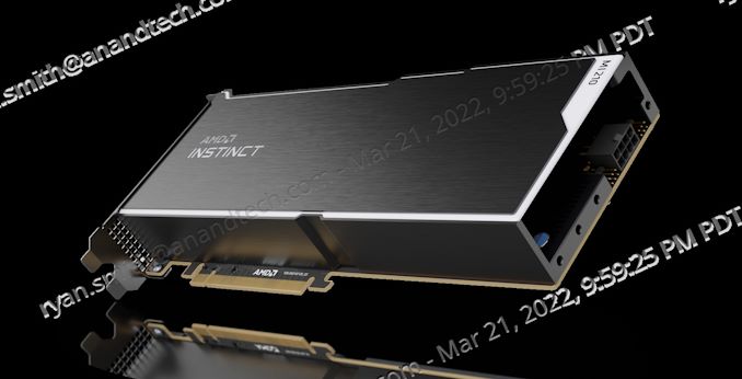
With both GDC and GTC going on this week, this is a big time for GPUs of all sorts. And today, AMD wants to get in on the game as well, with the release of the PCIe version of their MI200 accelerator family, the MI210.


First unveiled alongside the MI250 and MI250X back in November, when AMD initially launched the Instinct MI200 family, the MI210 is the third and final member of AMD’s latest generation of GPU-based accelerators. Bringing the CDNA 2 architecture into a PCIe card, the MI210 is being aimed at customers who are after the MI200 family’s HPC and machine learning performance, but need it in a standardized form factor for mainstream servers. Overall, the MI200 is being launched widely today as part of AMD moving the entire MI200 product stack to general availability for OEM customers.


AMD Instinct Accelerators
  MI250 MI210 MI100 MI50
Compute Units 2 x 10⁴ 104 120 60
Matrix Cores 2 x 416 416 480 N/A
Boost Clock 1700MHz 1700MHz 1502MHz 1725MHz
FP64 Vector 45.3 TFLOPS 22.6 TFLOPS 11.5 TFLOPS 6.6 TFLOPS
FP32 Vector 45.3 TFLOPS 22.6 TFLOPS 23.1 TFLOPS 13.3 TFLOPS
FP64 Matrix 90.5 TFLOPS 45.3 TFLOPS 11.5 TFLOPS 6.6 TFLOPS
FP32 Matrix 90.5 TFLOPS 45.3 TFLOPS 46.1 TFLOPS 13.3 TFLOPS
FP16 Matrix 362 TFLOPS 181 TFLOPS 184.6 TFLOPS 26.5 TFLOPS
INT8 Matrix 362.1 TOPS 181 TOPS 184.6 TOPS N/A
Memory Clock 3.2 Gbps HBM2E 3.2 Gbps HBM2E 2.4 Gbps HBM2 2.0 Gbps GDDR6
Memory Bus Width 8192-bit 4096-bit 4096-bit 4096-bit
Memory Bandwidth 3.2TBps 1.6TBps 1.23TBps 1.02TBps
VRAM 128GB 64GB 32GB 16GB
ECC Yes (Full) Yes (Full) Yes (Full) Yes (Full)
Infinity Fabric Links 6 3 3 N/A
CPU Coherency No N/A N/A N/A
TDP 560W 300W 300W 300W
Manufacturing Process TSMC N6 TSMC N6 TSMC 7nm TSMC 7nm
Transistor Count 2 x 29.1B 29.1B 25.6B 13.2B
Architecture CDNA 2 CDNA 2 CDNA (1) Vega
GPU 2 x CDNA 2 GCD

“Aldebaran”
CDNA 2 GCD

“Aldebaran”
CDNA 1 Vega 20
Form Factor OAM PCIe (4.0) PCIe (4.0) PCIe (4.0)
Launch Date 11/2021 03/2022 11/2020 11/2018


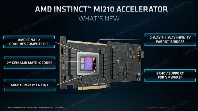
Starting with a look at the top-line specifications, the MI210 is an interesting variant to the existing MI250 accelerators. Whereas those two parts were based on a pair of Aldebaran (CDNA 2) dies in an MCM configuration on a single package, for MI210 AMD is paring everything back to a single die and related hardware. With MI250(X) requiring 560W in the OAM form factor, AMD essentially needed to halve the hardware anyhow to get things down to 300W for a PCIe card. So they’ve done so by ditching the second on-package die.


The net result is that the MI210 is essentially half of an MI250, both in regards to physical hardware and expected performance. The CNDA 2 Graphics Compute Die features the same 104 enabled CUs as on MI250, with the chip running at the same peak clockspeed of 1.7GHz. So workload scalability aside, the performance of the MI210 is for all practical purposes half of a MI250.


That halving goes for memory, as well. As MI250 paired 64GB of HBM2e memory with each GCD – for a total of 128GB of memory – MI210 brings that down to 64GB for the single GCD. AMD is using the same 3.2GHz HBM2e memory here, so the overall memory bandwidth for the chip is 1.6 TB/second.


In regards to performance, the use of a single Aldebaran die does make for some odd comparisons to AMD’s previous-generation PCIe card, the Radeon Instinct MI100. While clocked higher, the slightly reduced number of CUs relative to the MI100 means that for some workloads, the old accelerator is, at least on paper, a bit faster. In practice, MI210 has more memory and more memory bandwidth, so it should still have the performance edge the real world, but it’s going to be close. In workloads that can’t take advantage of CDNA 2’s architectural improvements, MI210 is not going to be a step up from MI100.


All of this underscores the overall similarity between the CDNA (1) and CDNA 2 architectures, and how developers need to make use of CDNA 2’s new features to get the most out of the hardware. Where CDNA 2 shines in comparison to CDNA (1) is with FP64 vector workloads, FP64 matrix workloads, and packed FP32 vector workloads. All three use cases benefit from AMD doubling the width of their ALUs to a full 64-bits wide, allowing FP64 operations to be processed at full speed. Meanwhile, when FP32 operations are packed together to completely fill the wider ALU, then they too can benefit from the new ALUs.


But, as we noted in our initial MI250 discussion, like all packed instruction formats, packed FP32 isn’t free. Developers and libraries need to be coded to take advantage of it; packed operands need to be adjacent and aligned to even registers. For software being written specifically for the architecture (e.g. Frontier), this is easily enough done, but more portable software will need updated to take this into account. And it’s for that reason that AMD wisely still advertises its FP32 vector performance at full rate (22.6 TFLOPS), rather than assuming the use of packed instructions.


The launch of the MI210 also marks the introduction of AMD’s improved matrix cores into a PCIe card. For CDNA 2, they’ve been expanded to allow full-speed FP64 matrix operation, bringing them up to the same 256 FLOPS rate as FP32 matrix operations, a 4x improvement over the old 64 FLOPS/clock/CU rate.


AMD GPU Throughput Rates

(FLOPS/clock/CU)
  CDNA 2 CDNA (1) Vega 20
FP64 Vector 128 64 64
FP32 Vector 128 128 128
Packed FP32 Vector 256 N/A N/A
FP64 Matrix 256 64 64
FP32 Matrix 256 256 128
FP16 Matrix 1024 1024 256
BF16 Matrix 1024 512 N/A
INT8 Matrix 1024 1024 N/A


Moving on, the PCIe format MI210 also gets a trio of Infinity Fabric 3.0 links along the top of the card, just like the MI100. This allows an MI210 card to be linked up with one or three other cards, forming a 2 or 4-way cluster of cards. Meanwhile, backhaul to the CPU or any other PCIe devices is provided via a PCIe 4.0 x16 connection, which is being powered by one of the flexible IF links from the GCD.


As previously mentioned, the TDP for the MI210 is set at 300W, the same level as the MI100 and MI50 before it – and essentially the limit for a PCIe server card. Like most server accelerators, this is fully passive dual slot card design, relying on significant airflow from the server chassis to keep things cool.  The GPU itself is powered by a combination of the PCIe slot and an 8 pin, EPS12V connector at the rear of the card.


Otherwise, despite the change in form factors, AMD is going after much the same market with MI210 as they have MI250(X). Which is to say HPC users who specifically need a fast FP64 accelerator. Thanks to its heritage as a chip designed first and foremost for supercomputers (i.e. Frontier), the MI200 family currently stands alone in its FP64 vector and FP64 matrix performance, as rival GPUs have focused instead on improving performance at the lower precisions used in most industry/non-scientific workloads. Though even at lower precisions, the MI200 family is nothing to sneeze at with tis 1024 FLOPS-per-CU rate on FP16 and BF16 matrix operations.


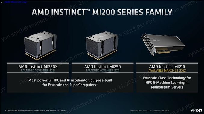
Wrapping things up, MI210 is slated to become available today from AMD’s usual server partners, including ASUS, Dell, Supermicro, HPE, and Lenovo. Those vendors are now also offering servers based on AMD’s MI250(X) accelerators, so AMD’s more mainstream customers will have access to systems based on AMD’s full lineup of MI200 accelerators.


Source: AnandTech – AMD Releases Instinct MI210 Accelerator: CDNA 2 On a PCIe Card

AMD Releases Milan-X CPUs With 3D V-Cache: EPYC 7003 Up to 64 Cores and 768 MB L3 Cache

There’s been a lot of focus on how both Intel and AMD are planning for the future in packaging their dies to increase overall performance and mitigate higher manufacturing costs. For AMD, that next step has been V-cache, an additional L3 cache (SRAM) chiplet that’s designed to be 3D die stacked on top of an existing Zen 3 chiplet, tripling the total about of L3 cache available. Now AMD’s V-cache technology is finally becoming available to the mass market, as AMD’s EPYC 7003X “Milan-X” server CPUs have now reached general availability.


As first announced late last year, AMD is bringing its 3D V-Cache technology to the enterprise market through Milan-X, an advanced variant of its current-generation 3rd Gen Milan-based EPYC 7003 processors. AMD is launching four new processors ranging from 16-cores to 64-cores, all of them with Zen 3 cores and 768 MB of stacked L3 3D V-Cache.


Source: AnandTech – AMD Releases Milan-X CPUs With 3D V-Cache: EPYC 7003 Up to 64 Cores and 768 MB L3 Cache

Cincoze DS-1300 Industrial PC Review: Xeon-Powered Do-it-All

Industrial PCs are meant for 24×7 deployment in a wide range of environments. This brings in a host of requirements such as wide operating temperature range, ruggedness, regulatory requirements, support for specific I/O types, etc. Most industrial PCs are passively cooled, with the absence of moving parts contributing to better reliability. In certain cases, processing power requirements and space constraints make it necessary to include active cooling. Today, we are looking at a high-end industrial PC from Cincoze – the DS-1300 featuring a Comet Lake-based Xeon CPU and a discrete GPU. Read on to for a detailed look at the features and performance profile of the flagship member of the Cincoze DS-1300 series.


Source: AnandTech – Cincoze DS-1300 Industrial PC Review: Xeon-Powered Do-it-All

Mushkin Redline VORTEX PCIe 4.0 NVMe SSD Launched: Affordable Flagship

Mushkin’s lineup of PCIe 4.0 SSDs has largely remained a Phison affair. The Delta series was based on the Phison E16 and the Gamma on the Phison E18. Recently, the company launched a new series of PCIe 4.0 SSDs – the Redline VORTEX. The key here seems to be the usage of a new SSD controller – the Innogrit Rainier IG5236. It appears to be taking over the flagship mantle from the Gamma – besting it in both read and write random access IOPS and also sequential read speeds. However, unlike the Delta and Gamma, which came to the market in 1TB, 2TB, and 4TB flavors, the Redline VORTEX series has three capacity points – 512GB, 1TB, and 2TB. Detailed specifications are provided in the table below.


<!–

–>


Mushkin Redline VORTEX SSD Specifications
Capacity 512 GB 1024 GB 2048 GB
Controller Innogrit IG5236
NAND Flash ?? 3D TLC NAND
Form-Factor, Interface Single-Sided M.2-2280, PCIe 4.0 x4, NVMe 1.4 Double-Sided M.2-2280, PCIe 4.0 x4, NVMe 1.4
DRAM 512 MB DDR4 1 GB DDR4 2 GB DDR4
Sequential Read 6750 MB/s 7430 MB/s 7415 MB/s
Sequential Write 2635 MB/s 5300 MB/s 6800 MB/s
Random Read IOPS 200K 390K 730K
Random Write IOPS 645K 1085K 1500K
SLC Caching Yes
TCG Opal Encryption No
Warranty 5 years
Write Endurance 250 TBW

0.27 DWPD
500 TBW

0.27 DWPD
1000 TBW

0.27 DWPD
MSRP $78 (15.23¢/GB) $125 (12.21¢/GB) ??


The SSD adopts a graphene heat dissipating label for its thermal solution – typical for the price point targeted. The performance numbers (aided by dynamic SLC caching) make it sitable for content creation and gaming – workloads that typically benefit from the capabilities provided by PCIe 4.0 SSDs.


Mushkin is not the first to market with the Innogrit Rainier controller. The Patriot Viper VP4300 series and the ADATA XPG GAMMIX S70 Blade were introduced late last year. While the Viper VP4300 is priced quite high, the Mushkin Redline VORTEX manages to undercut the XPG GAMMIX S70 blade by $12 at the 512GB capacity point and $5 at the 1TB point (based on current street pricing). The company is yet to announce availability and pricing for the 2TB SKU. The appearance of more affordable PCIe 4.0 NVMe SSDs in the market is good news for consumers.


Source: AnandTech – Mushkin Redline VORTEX PCIe 4.0 NVMe SSD Launched: Affordable Flagship

AMD Teases FSR 2.0: Temporal Upscaling Tech for Games Coming in Q2

Alongside their spring driver update, AMD this morning is also unveiling the first nugget of information about the next generation of their FidelityFX Super Resolution (FSR) technology. Dubbed FSR 2.0, the next generation of AMD’s upscaling technology will be taking the logical leap into adding temporal data, giving FSR more data to work with, and thus improving its ability to generate details. And, while AMD is being coy with details for today’s early teaser, at a high level this technology should put AMD much closer to competing with NVIDIA’s temporal-based DLSS 2.0 upscaling technology, as well as Intel’s forthcoming XeSS upscaling tech.


Source: AnandTech – AMD Teases FSR 2.0: Temporal Upscaling Tech for Games Coming in Q2

AMD Releases Adrenalin Software Spring 2022 Update: Adds RSR Upscaling and More

AMD this morning is releasing the awaited spring update to their AMD Software Adrenalin Edition suite for their GPUs. First unveiled back in January as part of AMD’s keynote address, the spring update (22.3.1) introduces a few quality-of-life features for AMD’s software stack, and is being headlined by the first release of AMD’s FSR 1.0-based Radeon Super Resolution (RSR) technology for driver-based game upscaling.


Source: AnandTech – AMD Releases Adrenalin Software Spring 2022 Update: Adds RSR Upscaling and More

AMD's Ryzen 7 5800X3D Launches April 20th, Plus 6 New Low & Mid-Range Ryzen Chips

Since the launch of AMD’s Zen 3-powered Ryzen 5000 desktop processors in late 2020, the company’s retail desktop chip offerings have been rather static. With AMD facing heavy demand for products on multiple fronts – from CPUs to GPUs to console APUs – and all during an unprecedented chip crunch, the company has held back on expanding its desktop offerings. Instead, AMD has focused its limited TSMC 7nm wafer allocations on trying to keep up with demand for some of their most important (and highest margin) products, such as server CPUs, laptop chips, and high-end desktop CPUs.


However, as the chip crunch has ever-so-slightly abated, AMD is now turning their attention back to the desktop space, to finally focus on fleshing out their desktop processor product lineups. We saw our first glimpse of that last week with the announcement of the long-awaited Threadripper Pro 5000 series for workstations. And now for this week the company is announcing the launch dates of several new Ryzen desktop processors, including the much-awaited Ryzen 7 5800X3D with V-Cache, as well as 6 new low-to-mid-range Ryzen SKUs for the retail market.


Source: AnandTech – AMD’s Ryzen 7 5800X3D Launches April 20th, Plus 6 New Low & Mid-Range Ryzen Chips

The ADATA XPG Cybercore 1300W PSU Review: Advanced From the Start

In today’s review, we are taking a look at XPG’s latest creation, the Cybercore power supply series. The Cybercore PSU is based on a whole new power supply platform and boasts a massive power output for its proportions, all while it is built exclusively with premium components.


Source: AnandTech – The ADATA XPG Cybercore 1300W PSU Review: Advanced From the Start

The Intel W680 Chipset Overview: Alder Lake Workstations Get ECC Memory and Overclocking Support

Earlier this month Intel quietly launched its W680 chipset, the company’s workstation-focused chipset for its 12th Gen Core (Alder Lake) processors. Unlike the current generation of consumer desktop chipsets such as Z690, H670, B660, and H610, the W680 adds the capability to use ECC DRAM, including both DDR5 and DDR4 variants. At present, there haven’t been many W680 motherboard announcements, although a couple of vendors, including ASRock Industrial and Supermicro have a few options listed. So we’re giving you the lowdown on W680, what it has to offer, and what technologies it brings for users looking to build a workstation-class desktop with Intel’s latest Alder Lake architecture.


Source: AnandTech – The Intel W680 Chipset Overview: Alder Lake Workstations Get ECC Memory and Overclocking Support