The SilentiumPC Fera 5 CPU Cooler Review: Quiet Cooling on a Budget

In today’s review, we are taking a look at the Fera 5 tower CPU cooler from SilentiumPC.


SilentiumPC’s main focus is to design and produce products with a very good price-to-performance ratio – which is to say, budget products for the mainstream market. The Fera 5 CPU cooler, in turn, embodies those ideals, with a focus on effective and quiet cooling from a cooler that sells for around €30. And while a budget cooler isn’t going to chart new territory in the CPU cooling space, as we’ll see, SilentiumPC has been able to strike a solid balance between performance and price, delivering a tower cooler that is notably quieter than typical budget coolers.


Source: AnandTech – The SilentiumPC Fera 5 CPU Cooler Review: Quiet Cooling on a Budget

GIGABYTE Issues Recall on Z690I Aorus Ultra Motherboards, Citing PCIe Gen 4 Issues

GIGABYTE has officially announced that it is offering an RMA replacement service for users that have purchased one of its key mini-ITX models for Intel’s 12th Gen Core series processors, the Z690I Aorus Ultra. With reports of numerous users experiencing compatibility and crashing issues when using PCIe 4.0 graphics cards on the board’s single full-length slot, GIGABYTE has opened up a special returns program for specific customers to offer a replacement board with the particular PCIe Gen 4 issue fixed.


On its website, GIGABYTE announced publically that it had investigated reports of customers experiencing issues with the Z690I Aorus Ultra and concluded that the PCIe 4.0 slot isn’t working as intended. Users’ fundamental problems when using the GIGABYTE Z690I Aorus Ultra came through a WHEA PCIe error, WHEA being short for Windows Hardware Error Architecture, which is designed to report errors when a system is experiencing instability. 


The front page of the GIGABYTE Z690I Aorus Ultra Customer Exchange/Refund Request Form


The ‘special’ program applies to all of its customers who purchased the Z690I Aorus Ultra, including the DDR5 and DDR4 variants, from non-third-party retailers such as Micro Center. GIGABYTE says the program will run until November 30th, 2022, with customers being able to opt for either request a replacement board or a refund. Of course, some terms and conditions are attached to this, with users requiring a valid serial number and a purchase receipt to show that they purchased this from a qualifying retailer or online store. 


For users who do not (or cannot) swap, GIGABYTE has also offered a workaround for the WHEA PCIe error, albeit a suboptimal one. The fix consists of going into the BIOS by pressing either F2 or the Del key during post and forcing the PCIe slot to operate at Gen 3 speeds rather than the defaulted Gen 4 speeds. 


The link to the replacement/refund RMA service is here: https://member.aorus.com/z690i-aorus-ultra-exchange-refund


Source: GIGABYTE


Related Reading


Source: AnandTech – GIGABYTE Issues Recall on Z690I Aorus Ultra Motherboards, Citing PCIe Gen 4 Issues

Applied Materials Outlines Next-Gen Tools for 3nm and GAA Transistor Era

Last month Samsung Foundry quietly announced that it was set to begin producing chips using its 3GAE (3 nm-class, gate-all-around transistors, early) process technology in the second quarter. While the industry’s first 3 nm-class node with GAA transistors is a noteworthy achievement by itself, one thing that is particularly important is that to make GAA transistors efficiently, fabs have to be equipped with new production tools. Fittingly, Applied Materials has recently outlined their next generation of tools that will be used to enable Samsung (and other fabs) to build their first GAA chips.


Gate-All-Around Transistors: Solving Many Problems at Once


New process technologies should enable higher performance, lower power, and higher transistor density to meet requirements of chip designers. But this combination has been particularly hard to achieve in the recent years as shrinking transistor sizes lead to negative effects like leakage current. To keep scaling performance and voltages while minimizing transistor sizes, the industry began transition from planar to FinFET transistors (which increased the contact area between the channel of the transistor and the gate by making the gate taller) in 2012 and this type of transistors will stay with us for a long time. But the pace of FinFET-based nodes innovation is slowing down as negative aspects of transistors shrinking starting to kick in.


Ever since Intel introduced its 22 nm FinFET-based technology over a decade ago, chipmakers began to talk about the next inevitable step in transistor design, which is gate-all-around. As the name suggests, in GAAFETs channels are horizontal and are surrounded by gates around all four sides of the channels, which solves many problems associated with the leakage current. But this is not the only advantage: in nanosheet/nanoribbon-based GAAFETs it is possible to adjust channel width to get higher performance or reduce power consumption. Since Samsung’s 3GAE and 3GAP technologies use nanosheets, Samsung calls its GAAFETs multi-bridge channel field-effect transistors (MBCFETs) to emphasize that it does not use nanowires. Furthermore, Applied Materials claims that GAA architecture reduces transistor variability, which means improved yields and faster time-to-yield (at least as far as transistor performance is concerned) and reduces cell area by 20% to 30%.


While all chipmakers have been talking about GAAFETs and their advantages over FinFETs at various academia industry events, Samsung was the first company to announce a transition to the new type of transistors with its 4 nm node sometimes in 2022 ~ 2023. Eventually, the company’s plans changed a bit and in 2019 it unveiled its GAAFET-based 3GAE and 3GAP nodes with high volume manufacturing due in 2022 and 2023, respectively. Last year the company re-emphasized plans to kick off production using its 3GAE in 2022 and this quarter it said that volume production was set to start in Q2.


But Manufacturing Is Challenging


But production of chips using any leading-edge process technology is challenging and making products using Samsung’s MBCFET-based 3GAE node certainly poses some risks not only because we are talking about a 3 nm-class manufacturing process, but because manufacturing of GAA transistors is different than making FinFETs.


Channels of GAA transistors are shaped using lithography, epitaxy and selective materials removal, processes that enable chipmakers to fine-tune width and uniformity for optimum power and performance. Those epitaxial steps are considerably more complex when compared to those with FinFETs as manufacturers need to deposit the multi-layer gate oxide and metal gate stacks around the tiny 10 nm channels, which is a key challenge with GAAFETs. This is where Applied’s high-vacuum Integrated Materials Solution (IMS) systems come into play. 


Firstly, Applied’s Producer Selectra Selective Etch IMS tool removes unnecessary SiGe to isolate the gate from the source/drain and define channel width without damaging surrounding materials. Secondly, the Applied Centura Prime Epi IMS tool can deposit an ultra-thin gate oxide layer using integrated atomic layer deposition (ALD), thermal, plasma treatment, and metrology steps. Applied’s IMS can reduce gate oxide thickness by 1.5 angstroms compared to competing solution, which allows to make gates thicker and enable higher drive current and therefore transistor performance without increasing current leakage, which is a consequence of thin gates.


Applied introduced its first Selectra etching system in 2016 and since then has shipped over 1,000 chambers that are currently in use by its customers, so the industry is quite aware how to use them. While etching is a widely used process, its usage and importance will grow as the industry begins to transit to newer process technologies, including those based on GAA transistors. 


It is necessary to note that numbers shared by Applied Materials come from various companies (including TSMC and Qualcomm) and should not be applied exclusively to Samsung Foundry’s 3GAE and 3GAP nodes. Meanwhile, the general advantages of GAA/MBC/nanoribbon/nanosheet transistors, as well as challenges with their manufacturing, are similar for the whole industry.


Samsung’s 3GAE: +30% Performance, -45% Area


Speaking of advantages, Samsung expects its 3GAE process to offer a 30% performance increase or a 50% power consumption reduction, and a 45% area reduction when compared to 7LPP. Such tangible benefits may be enough to justify challenges associated with this transition in the short term.


For now, the use of 3GAE manufacturing technology that relies a brand-new transistor structure is challenging in general, as in addition to new electronic design automation (EDA) tools, Samsung will need to invent new IP, and adopt brand-new design rules. All of these things, when combined with new lithography, new etching, and new deposit steps are going to make Samsung’s transition difficult. 


But in exchange, it will start gaining experience with GAA transistors years ahead of Intel and TSMC, which may bring certain gains in the long-term future. Furthermore, experience with GAAFETs will be beneficial for Samsung’s DRAM manufacturing as memory greatly benefits from smaller cell sizes and higher transistor densities. 


Source: AnandTech – Applied Materials Outlines Next-Gen Tools for 3nm and GAA Transistor Era

AMD Prepares New "Raise The Game" Bundle – Rushing to Counter Falling Card Prices

As retail video card prices drop back down to more normal prices following 18 months of cryptocurrency-fueled madness, AMD and its partners are quickly finding themselves with a new concern: AMD video card prices are dropping too much. As Ethereum mining profitability has plummeted, so has the price on video cards, especially the highest margin cards at the high-end of AMD’s product stack. As a result, the company is undertaking a rapid effort to shore up video card prices by bringing back game bundles with a new Raise The Game campaign.

The tried and true tool for boosting the value of video cards in slower times, game bundles are a favored tactic of video card makers to improve the value of their product, allowing them to improve their competitiveness or value to the consumer without changing the hardware itself. With the street value of a new AAA PC game going for $60 – and video card makers paying far less than that via bulk purchases and in-kind advertising – video game bundles are a relatively cheap way to boost the value of a product or otherwise stave off a more painful price cut. And while game bundles are a common fixture in more normal times, there hasn’t been a need for them in the past year as video cards have been quickly selling out without the additional help.

But as normalicy returns to the video card market and demand for new cards from miners has all but dried up (Ethereum mining profitability is now back to its pre-2021 levels), video card sales have dropped significantly. And so have their prices: in the last 2 days alone, the cheapest Radeon RX 6900 XT on Newegg has dropped from $949 to $849, which now puts it a good $150 below AMD’s original MSRP.


Source: AnandTech – AMD Prepares New “Raise The Game” Bundle – Rushing to Counter Falling Card Prices

Intel Launches Alder Lake-HX Series Core Processors: 55W and PCIe 5.0 For High-End Mobile

Intel today is announcing a new range of mobile 12th Gen Core family processors designed for enthusiast and desktop-replacement class laptops, the Alder Lake-HX series. Focusing on the more performance-driven high-end models, the Alder Lake HX series transfers its hybrid desktop design (ADL-S) into a thinner BGA package with up 16 cores (8P+8E) that’s more suitable for mobile devices. And since it’s based on that desktop hardware, Alder Lake-HX also brings with it some additional features that were previously limited to the desktop, such as support for PCIe 5.0, as well as a more desktop-like base TDP of 55 Watts.

In January of this year, Intel launched its first Alder Lake 12th Gen Core mobile processor, the Alder Lake-H family. In February, it then announced more for the lower-powered market through its Alder Lake-P and Alder Lake-U series with up to 14 cores with a mixture of its Performance (P) and Efficiency (E) cores. Intel has now officially launched the more premium of its 12th Gen Core series for mobile, the Alder Lake-HX series with up to 16 cores (8P+8E), and its new memory and core overclocking technology.

The latest in Intel’s arsenal is designed for premium and enthusiast laptops, with seven new chips ranging from sixteen cores and twenty-four threads, all the way down to an eight-core and twelve thread SKU. According to Intel, the Alder Lake-HX series completes its Alder Lake mobile family, with options spanning many different markets using its hybrid 12th Gen Core architecture to deliver a significant range in mobile performance for enthusiasts, gamers, and workstation use cases.


Source: AnandTech – Intel Launches Alder Lake-HX Series Core Processors: 55W and PCIe 5.0 For High-End Mobile

Intel: Desktop Arc A-Series Launch Now Staggers in to Q3'22

Ahead of Intel’s Vision event this morning, the company has published a short update on the status of the ongoing launch of their Arc family of GPUs. Penned by VP and GM of Intel’s Visual Compute Group, Lisa Pearce, the blog post addresses a few questions around the Arc launch, and particularly when we should expect to see the launch of Intel’s first desktop cards.


Starting there first, Pearce has announced that the desktop Arc launch has for all practical purposes slipped, with Intel now outlining a more staggered approach to their desktop launch. The first Arc desktop products were previously slated to launch later in Q2, and while this technically remains true, Intel’s Q2 launch plans are now limited to the Chinese market. The worldwide launch of the first desktop Arc products will then follow that in Q3 of this year.


Furthermore, that initial launch is going to be limited to the low end (3-series) parts of the Arc product stack, all of which are based around the ACM-G11 GPU. This is the same GPU that’s being used in Intel’s first wave of mobile Arc products, as well, so like in mobile, Intel is starting small and working their way up on the desktop. The desktop launch of the rest of Intel’s stack, the mid-range Arc 5 and high-end Arc Arc 7 products, will then follow in late summer. This will be a worldwide launch, however Pearce is very careful to note that it’s initially for “OEMs and system integrators”, with a retail release to follow later.


Given Intel’s slow, regional-focused rollout of their first Arc mobile products, these developments are not entirely unexpected. As Pearce accurately notes in her blog post, Intel tends to launch low-end (and low-volume) parts in China first, which is something we saw last year with the release of Intel’s Iris Xe (DG1) products. Compared in particular to the North American and European markets, the Chinese market is far more weighted towards entry-level parts, and logistically it makes for an easier launch since this is where many boards and board components are made to begin with.


Intel Arc Launch Decoder
  Arc 3 Mobile Arc 5 & 7 Mobile Arc 3 Desktop Arc 5 & 7 Desktop
China: OEM Launched Early Summer Q2 Later This Summer
China; Retail After OEMs After OEMs
Rest of World: OEM Shipping Now Early Summer Q3 Later This Summer
Rest of World: Retail After OEMs After OEMs


Meanwhile, Pearce’s blog post also offers an update on the ongoing rollout of Intel’s Arc mobile products. Acknowledging that Arc 3 laptop shipments are behind schedule, according to Pearce Intel has been hamstrung by a combination of unspecified software issues and China’s significant COVID lockdowns. As a result, Arc 3 laptops are only now finally becoming available on a worldwide level.


With the kinks apparently worked out, Intel is now preparing for the launch of the first mobile Arc 5 and Arc 7 products. Like Arc 3, the mobile parts will debut first. According to Pearce, the first Arc 5 and Arc 7 laptops will be available early this summer, hinting at a post-Computex (and likely Q3) release.


Overall, Intel has been planning a relatively modest launch from the start, with just a bit over 4 million GPUs slated for 2022. So the silver lining to their multiple schedule delays, at least, is that the company is getting some of the kinks worked out of the process while they’re still dealing with what’s ultimately small potatoes.  With future generations the stakes will go up – and so will the expectations.


Source: AnandTech – Intel: Desktop Arc A-Series Launch Now Staggers in to Q3’22

AMD Releases Radeon RX 6950 XT, 6750 XT, and 6650 XT: A Bit More Speed For Spring

AMD this morning is taking the wraps off a trio of new Radeon RX 6000 series video cards to round out its product stack. Aimed at everything from the midrange to flagship markets, the new Radeon RX 6950 XT, RX 6750 XT, and RX 6650 XT are being released as a mid-generation kicker to the Radeon family, to give AMD’s most important cards one last boost in performance. Taking advantage of newer 18Gbps GDDR6 memory along with slightly improved clockspeeds, the new cards, being released today, promise modest performance gains while giving AMD a chance to show off what their RDNA2 GPU architecture can do after nearly 18 months of refinement.


Source: AnandTech – AMD Releases Radeon RX 6950 XT, 6750 XT, and 6650 XT: A Bit More Speed For Spring

Western Digital Announces 22TB CMR and 26TB SMR HDDs: 10 Platters plus ePMR

Western Digital is announcing the sampling of its new 22TB CMR and 26TB SMR hard drives today at its What’s Next Western Digital Event. As usual, the hyperscale cloud customers will get first dibs on these drives. The key takeaway from today’s presentation is that Western Digital doesn’t yet feel the need to bring heat-assisted magnetic recording (HAMR) into the picture. In fact, WD is doubling down on energy-assisted PMR (ePMR) technology and OptiNAND (introduced first in the 20TB CMR drives). WD is also continuing to use the triple-stage actuator that it started shipping in the first half of 2020 in the new drives. It goes without saying that the new high-capacity drives are helium-filled (HelioSeal technology). The main change common to both drives is the shift to a 10-stack design.


The SMR drives are getting an added capacity boost, thanks to WD’s new UltraSMR technology. This involves adoption of a new advanced error correction algorithm to go along with encoding of larger blocks. This allows improvement in the tracks-per-inch (TPI) metric, resulting in 2.6TB per platter. The new Ultrastar DC HC670 uses ten platters to provide 26TB of host-managed SMR storage for cloud service providers.


ArmorCache Technology


As part of the announcements, WD also provided additional details on the caching feature enabled by OptiNAND – ArmorCache. Last year’s announcement was quite light in terms of actual performance numbers, but the 20TB OptiNAND drives have been out in the market for a few quarters now.


The UFS-based iNAND package helps the OptiNAND-based HDDs deliver upwards of 80% improvement in IOPS for low-queue depth large-sized random writes (10% – 20% improvement for small-sized writes) in use-cases where the write cache is disabled. Since non-OptiNAND HDDs can only cache whatever can be flushed out to the serial flash during emergency power-off situations, the larger cache size afforded by the iNAND device relaxes this limitation considerably. As discussed in the OptiNAND announcement coverage last year, use-cases with write caching enabled benefit from the EPO data protection afforded by the iNAND device. Enabling write caching often requires hosts to send out cache flush commands to the HDDs. These commands require the HDD to stop accepting new commands until the completion of the flush, resulting in loss of performance. The ArmorCache makes these flush commands unnecessary, allowing the drive to be used with full performance with no risk of data loss due to EPO.


Concluding Remarks


The 22TB Ultrastar DC HC570 and 26TB Ultrastar DC HC670 are currently sampling to hyperscalers. Volume shipment of the CMR drive to the channel is set for the next quarter. The Ultrastar HC HC670 is a host-managed SMR drive, and will hence ship only to select customers around the same timeframe. Western Digital will be delivering variants of the CMR drive across its HDD portfolio – 22TB WD Purple Pro for surveillance NVRs, WD Red Pro for NAS systems, and WD Gold for SMB and enterprise customers in summer.


The updated capacity points – in particular, the jump in the SMR drive capacity – delivers clear TCO benefits to WD’s cloud customers. Crucially, WD believes it has enough trust in its ePMR setup to deliver 30TB+ HDDs without having to go the HAMR route. From a technology perspective, this will make the upcoming roadmap / product announcements from Seagate (HAMR deployment for publicly-available drives) and Toshiba (need for any technology beyond FC-MAMR) interesting to watch.


Source: AnandTech – Western Digital Announces 22TB CMR and 26TB SMR HDDs: 10 Platters plus ePMR

Western Digital Announces WD_BLACK SN850X NVMe and P40 Game Drive SSDs

Western Digital is announcing a host of consumer-focused SSD solutions today at its What’s Next Western Digital Event. The gaming-focused WD_BLACK is getting the SN850X NVMe SSD and the P40 Game Drive SSD, while the SN740 is now making an appearance as PCIe 4.0-capable M.2 2230 NVMe SSD under the regular Western Digital brand.


The WD_BLACK drives are slated for a summer release. The SN850X is a PCIe 4.0 x4 NVMe SSD with read speeds of up to 7300 MBps, and will be available in 1TB ($190 MSRP), 2TB, and 4TB capacities. The 1TB and 2TB models have an optional heat sink with RGB lighting included. Official datasheets with additional details are expected closer to launch in July 2022.


The P40 Game Drive SSD is a USB 3.2 Gen 2×2 (20Gbps) external drive that builds upon the P50 model by adding RGB lighting to the casing. It will be available in 500GB ($120 MSRP), 1TB, and 2TB capacities in summer 2022.


Western Digital also talked about the new ‘Game Mode 2.0’ feature in the WD_BLACK Dashboard for unlocking additional performance-boosting features on Windows PCs. This mode is available for the SN850X NVMe SSD. The dashboard software can also be used with the P40 Game Drive to control the RGB lighting.


Source: AnandTech – Western Digital Announces WD_BLACK SN850X NVMe and P40 Game Drive SSDs

SanDisk Professional PRO-BLADE Modular SSD Ecosystem Unveiled

Western Digital is announcing a host of products under the SanDisk and SanDisk Professional brands today at its What’s Next Western Digital Event. The company also provided a second look at products introduced during the recently concluded NAB show – the G-DRIVE PRO STUDIO SSD with a 7.68TB enterprise-class desktop SSD inside, and the addition of 20TB Ultrastar drives to the G-RAID SHUTTLE 8 (driving up the top capacity to 160TB).


The new products being announced today have been designed to address issues faced by high-volume content creators. The most exciting of the lot is the SanDisk Professional PRO-BLADE modular SSD ecosystem. Western Digital has created a compact enclosure for its PCIe 3.0 x4 NVMe SSDs (with a custom, but not proprietary connector). Two options are provided to connect this PRO-BLADE SSD Mag to a host system – the PRO-BLADE TRANSPORT is the portable sleeve with support for a single mag, while the PRO-BLADE STATION is the JBOD desktop version with support for up to four mags.


The target market for the PRO-BLADE products include professionals and prosumers requiring multiple high-speed portable drives for for content capture and backing up on the field, while needing quick transfers back at their editing desks. The lightweight high-capacity mags enable easy portability and consolidation of storage in use-cases previously restricted to heavy multi-HDD systems. Western Digital provided a real-world example where 42 lbs. worth of storage devices could be replaced by a set of drives weighing in at less than 7 lbs.


The company also pointed out the rising prevalence of professional capture devices with the ability to record directly to USB-C SSDs. The PRO-BLADE TRANSPORT can also be used directly with those cameras and the mag transferred directly to the JBOD PRO-BLADE STATION. The number of mags in use can vary based on the workflow requirements.


On the hardware front, the SSD Mag employs a 40-pin custom connector and has features to aid in easy hot-swapping. The enclosure is also designed to withstand drops (up to 3m) and has 4000lbs of crush resistance. The aluminum body also aids in heat dissipation. The mags are qualified for more than 2000 mating cycles with the TRANSPORT / STATION enclosures. The custom connector is designed to ensure no loss of the internal SSD’s native speeds – supporting up to 3GBps reads and 2.6GBps writes, with the actual value varying depending on the enclosure used.


The TRANSPORT enclosure employs a USB 3.2 Gen 2×2 (20Gbps) Type-C host interface and adds additional thermal protection to the mag’s aluminum enclosure. The desktop STATION enclosure has a Thunderbolt 3 host interface to support the mag’s maximum transfer rates and has additional thermal management in the form of active cooling and adequate ventilation slots.


The table above summarizes the key features of the products in the PRO-BLADE ecosystem.


On the SanDisk front, the company is announcing new Extreme PRO UHS-I cards in both SD and microSD form-factors. The key differentiation compared to previous UHS-I offerings is the ability to ingest data from these cards at up to 200MBps – almost double the UHS-I rates. SanDisk used to offer the previous generation Extreme PRO UHS-I cards with a 170MBps read speed rating using proprietary extensions, and the new cards have improved on this speed.


The higher speeds can be unlocked with the PRO-READER card reader that can be used with the PRO-DOCK4 announced in May 2021 during the launch of the SanDisk Professional brand. The cards work at normal UHS-I speeds when used with other card readers.


We are particularly excited about the PRO-BLADE SSD Mag and its custom connector. Given the non-proprietary nature, it would be interesting to see if NAS vendors adopt it. Currently, hot-swappable NVMe SSDs in SMB / SOHO NAS systems are restricted to the U.2 form-factors, and general M.2 support is available only directly on the NAS motherboard. The adoption of the PRO-BLADE mag’s form-factor could be a consumer-friendly option.


Source: AnandTech – SanDisk Professional PRO-BLADE Modular SSD Ecosystem Unveiled

AMD Announces Ryzen 5000 C-Series For High-End Chromebooks

In September 2020, AMD released its Ryzen 3000 C-series for Chromebooks, a line up of budget-priced chips based on the 12nm Picasso (Ryzen+) architecture that featured up to 4 cores and 8 threads and up to 11 Radeon Vega compute units. Nearly two years on and AMD has just announced four new Ryzen 5000 C-series SKUs designed to bring the performance benefits of its Cezanne (Zen 3) architecture to the Chromebook space.


The four new Ryzen 5000 C-series processors range from 8C/16T to 2C/4T, all with a 15 W TDP and designed to improve productivity and battery life over existing Ryzen 3000 C-series processors and Intel’s 11th Gen Tiger Lake chips.


Aimed at the premium area of the Chromebook market, the new AMD Ryzen 5000 C-series looks to offer OEMs and users premium options for the latest generation of Chromebooks with some higher-end features such as fast charging and Wi-Fi 6E networking capability.


AMD Ryzen 5000 C-Series For Chromebooks (Zen 3)
AnandTech Core/

Thread
Base

Freq
1T

Freq
L2/L3

Cache
iGPU iGPU

Freq
TDP
Ryzen 7 5825C 8 16 2000 4500 20 MB Vega 8 Up to 1.8 GHz 15 W
Ryzen 5 5625C 6 12 2300 4300 19 MB Vega 7 Up to 1.6 GHz 15 W
Ryzen 3 5425C 4 8 2700 4100 10 MB Vega 6 Up to 1.5 GHz 15 W
Ryzen 3 5125C 2 4 3000 3000 9 MB Vega 3 Up to 1.2 GHz 15 W


Looking at the specifications of the Ryzen 5000 C-series line-up, the top model is the Ryzen 7 5825C with an impressive 8 cores and 16 threads which is double that of the previous top-tier Chromebook Ryzen processor, the AMD Ryzen 7 3700C. It has a base core frequency of 2 GHz, with a boost core clock of up to 4.5 GHz on a single core, which is bolstered by its Radeon Vega 8 integrated graphics with a maximum boost frequency of up to 1.8 GHz.


The second model in the new line-up is the Ryzen 5 5625C, which has 6 cores, 12 threads, and integrated Radeon Vega 7 graphics with a maximum boost frequency of up to 1.6 GHz. The 6 cores feature a base frequency of 2.3 GHz, while one of these cores can boost up to 4.3 GHz for applications that demand additional performance.


Focusing on the two entry-level models in the line-up, the Ryzen 3 5425C benefits from 4 cores and 8 threads with a base frequency of 2.7 GHz, with a boost frequency on one core of up to 4.1 GHz, as well as AMD’s Radeon Vega 6 graphics that can boost up to 1.5 GHz. The Ryzen 3 5125C is the lowest in the new C-series stack with just 2 cores and 4 threads, has a consistent core clock speed of 3 GHz, and has 3 Vega graphics compute cores with a maximum boost frequency of up to 1.2 GHz.


As we go from top to bottom, each model in the line-up increases in base core frequency, while the boost clocks bar the Ryzen 3 5125C, which has a set core clock speed of 3 GHz, experience a drop in frequency. All the Ryzen 5000 C-series models feature a 15 W TDP envelope, so core frequency on both the Zen 3 cores and the Radeon Vega cores will depend on the application, task, or game being used to optimize the relative power envelope to fit within the 15 W TDP threshold.


While we don’t typically concern ourselves with vendor-given performance data, perhaps the most impressive of AMD’s claims is battery life. AMD is claiming that the Ryzen 5 5625C has up to improve battery life by 94% when directly compared to Intel’s Core i5-1135G7 processor, which, if true, is very impressive. One of the main benefits of the Chromebook series is usability, and having an improved battery life can increase overall productivity and lifespan when using it while traveling between charges.


So far, AMD has announced two of its partners already on board with its Ryzen 5000 C-series for Chromebooks, including HP and Acer. Both are launching new models due later on in the year, but AMD highlighted two new models:


HP Elite C645 G2 Chromebook


The first of the new Chromebooks to feature AMD’s Ryzen 7 5825C processor is the HP Elite C645 G2. HP is expected to offer multiple display options, including various configurations of its 14″ 1080p touchscreen panel and plenty of impressive features. These include support for up to 16 GB of LPDDR4X memory with up to 512 GB of PCIe storage. Other features include the latest Wi-Fi 6E wireless and BT 5.2 connectivity and an optional 4G LTE version. The HP Elite C645 will also have a 5 MP integrated webcam, a SmartCard terminal for a CAD-capable keyboard, and an SEC fingerprint sensor for added security.


The HP Elite C645 G2 Chromebook is expected to hit retail shelves in Q2 2022, with pricing currently unknown.


Acer Chromebook Spin 514


The second of the new Ryzen 5000 C-series Chromebooks is the Acer Chromebook Spin 514, which is a 2-in-1 convertible with a 14″ touchscreen. Acer is using the AMD Ryzen 7 5825C processor in this model, and it can support up to 256 GB of PCIe Gen 3 storage and support the latest Wi-FI 6E routers with BT 5.2 connectivity. Acer has specified that the Chromebook Spin 514 includes military-grade MIL-STD 810 durability with a Corning gorilla glass touchscreen panel that supports sRGB 100% color.


At the time of writing, Acer says the Chromebook Spin 514 will be available in Q3 2022, with expected pricing not disclosed.


It is expected that more vendors will adopt AMD’s Ryzen 5000 C-series processors for Chromebooks in the coming months, although these are OEM only, and pricing is currently unknown on each of the models.


Source: AMD


Source: AnandTech – AMD Announces Ryzen 5000 C-Series For High-End Chromebooks

Qualcomm Launches Wi-Fi 7 Networking Pro Series for 10Gbps Access Points

The last few months have seen multiple vendors launch products in the Wi-Fi 7 (802.11be) space. Mediatek demonstrated working 802.11be-compliant silicon under the Filogic lineup earlier this year. Concrete technical details and part numbers were not announced during the event. Last month, Broadcom introduced a comprehensive Wi-Fi 7 portfolio, detailing multiple 802.11be radios for access points, a networking SoC built keeping 802.11be bandwidth in mind, and a client radio for mobile applications.


Wi-Fi 7 / 802.11be Background


The 802.11 Working Group’s focus with 802.11be has been on extremely high throughput. This has been achieved primarily through a combination of three different aspects:


  • Support for up to 16 spatial streams
  • Support for channel widths up to 320MHz (with operation in 2.4 GHz, 5 GHz, and 6 GHz bands)
  • Support for 4096-QAM (4K-QAM) resulting in better utilization of available spectrum (a faster modulation / coding scheme).


It must be noted that wider channels are available only in the 5 GHz and 6 GHz bands.


Theoretically, these aspects allow for up to around 46 Gbps of wireless throughput. 802.11be also aims to enable usage of Wi-Fi for real-time applications by including features for low-latency communications such as Multi-link operation (MLO). This allows a client and an access point to simultaneously communicate over multiple channels that might even belong to different bands.


The 802.11be specifications also allow for better performance in environments with heavy interference by permitting adaptive puncturing – the desired channel need not be necessarily contiguous. This improves on the preamble puncturing feature already available as part of the 802.11ax specifications.


Interference and co-existence with non-Wi-Fi users of the same spectrum is handled using automatic frequency coordination (AFC). Unlike the Open AFC initiative (of which Broadcom is a part), Qualcomm is opting to provide its own turnkey solution for its customers.


As expected, AFC will require the device agent to be connected to the Internet for channel configuration and power modulation purposes.


Qualcomm’s Wi-Fi 7 Portfolio


At MWC 2022, Qualcomm had provided details of their 802.11be client silicon targeting mobile devices. The FastConnect 7800 is expected to become available in H2 2022, and integrates Bluetooth 5.3 support with key Wi-Fi 7 features. Today, the company is introducing its Wi-Fi 7 Networking Pro Series access point platforms to expand its Wi-Fi 7 portfolio.


Qualcomm started marketing its Wi-Fi solutions under the Networking Pro and FastConnect monikers back in 2019, with the launch of its Wi-Fi 6 solutions. The 2nd generation products catered to the Wi-Fi 6E ecosystem, and it comes as no surprise that today’s 3rd Gen. launch focuses on Wi-Fi 7.


The introduction of the Networking Pro tag has contributed to opaqueness in the composition of the router / AP platforms from a end-consumer perspective. Unlike Broadcom’s public announcement of core details of the networking SoC, and characteristics of the various radio options for its reference designs, Qualcomm provides these details only to their customers. Eventually, these details do become public after market availability of the products. For example, the Networking Pro 800 platform’s breakdown is available here – we see a core WiSoC with integrated MAC and baseband coupled with discrete radios. Therefore, it is disappointing that Qualcomm has not given us much to analyze in today’s announcements beyond basic product specifications. These high-level feature specifications match the features in Broadcom’s products announced last month.


It must be noted that Qualcomm also provides the ‘Immersive Home’ platform for entry-level Wi-Fi routers. These are typically similar to the ‘Networking Pro’ platforms, except for cut-down stream counts and reduced WiSoC capabilities in terms of CPU core counts and frequencies. Given that Qualcomm refused to provide any details of CPU core counts or frequencies for the Networking Pro series being launched today, we need to wait for an official announcement related to their Wi-Fi 7 portfolio for the cost-sensitive segment.


The 3rd Gen. Networking Pro series consists of four members, with stream counts ranging from 6 in the Networking Pro 620 to 16 in the Networking Pro 1620. Radio options exist for two or four streams in each of the 2.4 GHz, 5 GHz, and 6 GHz bands.


Qualcomm claims peak system PHY rates of up to 33 Gbps, and per-channel wireless PHY rates of more than 10 Gbps, with the capability of supporting more than 500 users in each channel.


The availability of 6 GHz spectrum for Wi-Fi is not universal. Qualcomm indicated that different configurations of the Networking Pro 3rd Gen series are possible, based on the allocation.


Qualcomm’s Wi-Fi 7 Networking Pro series will allow its customers to create a wide range of enterprise-class and premium wireless access points / routers. The platforms are already sampling – we should be seeing market availability of BE10000, BE16000, BE21000, and BE33000 Wi-Fi routers based on them in a few quarters.


5G-based fixed wireless access is fast becoming an attractive option for many consumers – sometimes even as the primary broadband connection. Qualcomm’s strengths in 5G will act as an asset from a bundling perspective for integrated Wi-Fi 7 / 5G platforms. However, Broadcom has significant presence with service providers for 10G PON and DOCSIS 4.0. It is likely that those high-speed ISPs will find Broadcom’s possible bundled offerings attractive for their Wi-Fi 7-capable consumer gateways. While we wait for Mediatek and MaxLinear (to whom Intel sold their Home Gateway Platform Division) to reveal their Wi-Fi 7 cards fully, it appears that initial battle will be between products based on Qualcomm’s 3rd Gen. Networking Pro series and those using Broadcom’s Wi-Fi 7 portfolio.


Source: AnandTech – Qualcomm Launches Wi-Fi 7 Networking Pro Series for 10Gbps Access Points

VESA Launches Variable Refresh Display Performance Standards: AdaptiveSync and MediaSync

Kicking off what’s set to be a busy May, this morning the Video Electronics Standards Association (VESA), the PC display industry’s primary consortium, is rolling out a new set of performance standards for variable refresh rate displays. Dubbed AdaptiveSync and MediaSync, these new test standards are designed to offer an industry-neural and open specification for the behavior and performance of DisplayPort displays. AdaptiveSync is a standard designed for high-end gaming displays, while MediaSync is aimed at eliminating video jitter on a much wider array of devices.


Source: AnandTech – VESA Launches Variable Refresh Display Performance Standards: AdaptiveSync and MediaSync

Intel: Meteor Lake Chiplet SoC Up and Running

Alongside Intel’s regular earnings report yesterday, the company also delivered a brief up on the state of one of their most important upcoming products, Meteor Lake. Intel’s first chiplet/tile-based SoC, which completed initial development last year, has now completed power-on testing and more. The news is not unexpected, but for Intel it still marks a notable milestone, and is important proof that both Meteor Lake and the Intel 4 process remain on track.


Meteor Lake, which is slated to be the basis of Intel’s 14th generation Core processors in 2023, is an important chip for the company on several levels. In terms of design, it is the first chiplet-based (or as Intel likes to put it, “disaggregated”) mass-market client SoC from the company. Intel’s roadmap for the Core lineup has the company using chiplet-style SoCs on a permanent basis going forward, so Meteor Lake is very important for Intel’s design and architecture teams as it’s going to be their first crack at client chiplets – and proof as to whether they can successfully pull it off.


Meanwhile Meteor Lake is also the first client part that will be built on the Intel 4 process, which was formerly known as Intel’s 7nm process. Intel 4 will mark Intel’s long-awaited (and delayed) transition to using EUV in patterning, making it one of the most significant changes to Intel’s fab technology since the company added FinFETs a decade ago. Given Intel’s fab troubles over the past few years, the company is understandably eager to show off any proof that its fab development cycle is back on track, and that they are going to make their previously declared manufacturing milestones.


As for this week’s power-on announcement, this is in-line with Intel’s earlier expectations. At the company’s 2022 investor meeting back in February, in the client roadmap presentation Intel indicated that they were aiming for a Q2’22 power-on.


In fact, it would seem that Intel has slightly exceeded their own goals. While in a tweet put out today by Michelle Johnston Holthaus, the recently named EVP and GM of Intel’s Client Computing Group, announced that Meteor Lake had been powered on, comments from CEO Pat Gelsinger indicate that Meteor Lake is doing even better than that. According to Gelsinger’s comments on yesterday’s earnings call, Meteor Lake has also been able to boot Windows, Chrome, and Linux. So while there remains many months of bring-up left to go, it would seem that Meteor Lake’s development is proceeding apace.


But that will be a story for 2023. Intel will first be getting Raptor Lake out the door later this year. The Alder Lake successor is being built on the same Intel 7 process as Alder Lake itself, and will feature an enhanced version of the Alder Lake architecture.


Source: AnandTech – Intel: Meteor Lake Chiplet SoC Up and Running

Intel Reports Q1 2022 Earnings: Improved Enterprise Sales Buoy Weaker Client Revenue

Kicking off our coverage of the first earnings season of the year for the tech industry, we as always start with Intel. The blue-hued blue-chip company is the first out of the gate to report their results for the first quarter of 2022, with Intel reporting something of a mixed quarter. With revenue down on a yearly basis – thanks in large part to softer client sales – Intel is no longer on a hot streak of setting records. At the same time, however, the company has dialed back its lofty expectations accordingly, and as a result was still able to slightly edge out its Q1 guidance.

For the first quarter of 2022, Intel booked $18.4B in revenue, a drop of 7% from the year-ago quarter. Buffering the company against this revenue drop on a GAAP basis has been an improvement in both operating income and net income, both of which benefitted from some one-off restructuring and investment gains (McAfee equity sale). As a result, Intel booked $8.1B in net income on a GAAP basis, which is a 141% improvement on the year. Otherwise, stripping things back to non-GAAP financials, things more closely mirror the overall revenue picture with a 35% decline in income.


Source: AnandTech – Intel Reports Q1 2022 Earnings: Improved Enterprise Sales Buoy Weaker Client Revenue

Solidigm Launches First Post-Intel Enterprise SSDs: D7-P5620 and D7-P5520

Back in late 2021, Intel and SK hynix completed the first stage of their long-awaited transfer of Intel’s NAND (and NAND-based SSD) business to SK hynix. That company, in turn, took Intel’s NAND SSD assets and put them under their own subsidiary, Solidigm, who took over sales of Intel’s existing SSD portfolio. Now, a few months later, Solidigm is gearing up to release its first post-Intel SSDs, the enterprise-focused D7-P5520 and D7-P5620.


Diving right into matters, Solidigm is essentially picking up right where Intel left off, both in regards to product design and product naming. Intel was already seeing solid market penetration with its D-series branding, so there’s little reason to give up a good thing for the new Solidigm. In any case, the new drives are designed and marketed to slot right in as the next-generation parts in the D7 lineup, which is Solidigm’s highest performance drives for the enterprise and server market.


From a pure specification standpoint, the big news with the latest generation of drives is that Solidigm has doubled their capacities. The D7-P5620 will be available in capacities from 1.6TB to 12.8TB, while the D7-P5520 will go up to 15.36TB for its larger form factor drives. At this point Solidigm has not announced what NAND they’re using, but as we haven’t heard anything about the company launching their 5th generation NAND to replace their current 144L TLC tech, presumably that’s what’s being used here – especially as Intel/Solidigm never released a 144L P5600 series drive.


Solidigm Enterprise SSDs
  D7-P5620 D7-P5600 D7-P5520 D7-P5510
Form Factor U.2 2.5″ 15mm U.2 2.5″ 15mm

E1.S 9.5mm/15mm

E1.L 9.5mm
U.2 2.5″ 15mm
Interface PCIe 4.0 NVMe 1.3c
Capacities 1.6TB

3.2TB

6.4TB

12.8TB
1.6TB

3.2TB

6.4TB
1.92TB

3.68TB

7.68TB

15.36TB (U.2 & E1L)
3.68TB

7.68TB
NAND Solidigm 144L TLC? Intel 96L TLC Solidigm 144L TLC? Intel 144L TLC
Sequential Read 7100 MB/s 7000 MB/s 7100 MB/s 7000 MB/s
Sequential Write 4200 MB/s 4300 MB/s 4200 MB/s 4200 MB/s
Random Read (4 kB) 1.1M IOPS 1M IOPS 1.1M IOPS 930k IOPS
Random Write (4 kB) 220k IOPS 260k IOPS 220k IOPS 190k IOPS
Write Endurance 3 DWPD 3 DWPD 1 DWPD 1 DWPD


As with earlier iterations of the D7 family, both drives are built from the same platform – meaning the same controller, NAND, and firmware. The only configuration difference between the drives is the amount of overprovisioning, with the P5600 drives using 20% overprovisioning to ensure faster performance, while the P5500 drives use just 4% overprovisioning to maximize capacity. Consequently, the P5620 is being pitched by the company as a mixed workload (mixed read/write) drive that can sustain up to 3 DWPD, while the P5520 is aimed at workloads with more reads than writes, with a 1 DWPD endurance.


Despite the difference in overprovisioning, both drives officially carry the same rated write performance: 4.2GB/second for large sequential writes, and random write IOPS of 220K. In the case of the P5620, this is actually a slight downgrade from the original P5600, though not entirely unexpected given the shift from 96L NAND to what’s presumably 144L NAND. Meanwhile read speeds are up slightly across the board, with both drives topping out at 1.1M read IOPS, or 7.1GB/second sequential.


We don’t have any additional information from the company on the controller used, however based on the specifications, at this juncture there’s nothing to indicate it’s significantly different from the existing Arbordale Plus controller. Though it sounds like Solidigm may be tweaking things in firmware slightly differently than Intel did, as Solidigm is focusing on read latency (especially reads under write pressure) more than Intel. In the case of the P5500 series, they’ve knocked 4K read latency down from 84μs to 75μs for the P5520; meanwhile write latency has seen a smaller drop, saving off 1μs to bring it down to 15μs.


The launch of the P5520 also marks the significantly overdue introduction of EDSFF form factors for some of the D7 series drives. Along with the classic U.2 form factor that the drives have used for the last few generations, the P5520 will also be available in the E1.L and E1.S form factors. The latter is new territory for Solidigm, as even in the company’s lower-ender/higher-density D5 product lineup, they’ve only used E1.L previously. The P5520 E1.S drives, in turn, will actually come in two sizes: E1.S 9.5mm and E1.S 15mm. Both will offer the same reduced capacities – 7.68TB max versus double that for U2/E1.L – however the 15mm drive will use that space for a heatsink that the 9.5mm drive lacks the room to fit. Otherwise, the P5620 remains unchanged, and will only come in the U.2 form factor.


Wrapping things up, according to Solidigm the drives are already in mass production, and are even deployed with some OEMs and cloud providers.


Source: AnandTech – Solidigm Launches First Post-Intel Enterprise SSDs: D7-P5620 and D7-P5520

Kioxia Announces XG8 Client SSDs: PCIe 4.0 and BiCS5 For OEMs

Kioxia this morning is rolling out its next-generation of full-size client SSDs, the XG8 family. Like its predecessors, the XG8 is aimed at the OEM market, for customers who are after a full M.2 2280-sized drive and are looking for better performance than the company’s more integrated and compact BG-series drives. Notable features for the latest-generation drive include a PCIe 4.0-capable controller, as well as capacities as high as 4TB.


And while we’d normally use the company’s previous-generation drive as a baseline to illustrate what’s new with the latest drive, today’s announcement of the XG8 is a bit weird, even by Kioxia’s own OEM-centric standards. The predecessor to the XG8 is the XG7, which was launched in November of 2020 with a very similar feature set: a PCIe 4.0 M.2 2280 SSD with capacities up to 4TB. However, for reasons we’re still not entirely clear on, the XG7 only saw a very limited deployment among OEMs, to the point that Kioxia never even put together a proper product page for the part. As a result, the company is taking a mulligan of sorts and is starting fresh with the XG8, positioning it as the successor to the PCIe 3/BiCS4-based XG6.


Kioxia XG8 SSD Specifications
Capacity 512 GB 1 TB 2 TB 4 TB
Form Factor M.2 2280
Interface PCIe Gen4 x4, NVMe 1.4
NAND Flash 112L BiCS5 3D TLC


Starting with the basics, the XG8 is a M.2 2280 form factor SSD with a PCIe 4.0 x4 connection. Kioxia is using their 5th generation, 112-layer BiCS5 NAND, with capacities ranging from 512GB up to 4TB. That NAND is being paired with their own in-house controller, which offers NVMe 1.4 support as well as the option for the usual OEM-centric security features such as TCG Pyrite 2.01 and TCG Opal 2.01.


Kioxia classifies the drive as a high-end product – particularly in relation to the BG5 – though as this is again by OEM standards, it’s a bit up in the air by enthusiast standards. Unfortunately, Kioxia isn’t providing any hard performance figures in advance of today’s announcement, so we don’t even have on-paper numbers to go by. For the moment, Kioxia is primarily throwing around 2x the performance of the XG6, most of which I’d expect to come from the switch to PCIe 4.0 and the additional host-to-controller bandwidth that affords.


Based on the lack of specification information and the fact that so many figures line up with the absentee XG7, it’s not at all clear what sets the XG8 apart from its more recent sibling. Presumably something has changed, if only to avoid another misfire, but at this point we’d just be guessing. Though it is notable that this drive family appears to be doing away with the ‘P’ designation that Kioxia used for high capacity drives in previous generations (e.g. XG6-P), as there is no mention of that sub-family of drives this time around.


Finally, this is probably one of the last BiCS5 client drives we’ll see from Kioxia. The WD/Kioxia joint venture has been producing BiCS5 NAND since late 2020, and according to recent WD earnings calls, 162L BiCS6 is expected to go into mass production late this year.


In the meantime, the XG8 is now sampling to Kioxia’s customers, and should start showing up in OEM laptops and desktops soon.


Source: AnandTech – Kioxia Announces XG8 Client SSDs: PCIe 4.0 and BiCS5 For OEMs

TSMC Roadmap Update: N3E in 2024, N2 in 2026, Major Changes Incoming

Taiwan Semiconductor Manufacturing Co. has solid plans for the next few years, but the foundry’s manufacturing technology design cycles are getting longer. As a result, to address all of its clients’ needs, the company will have to keep offering half-nodes, enhanced, and specialized versions of its fabrication processes.


TSMC’s success in the last 20 years or so was largely conditioned by the company’s ability to offer a new manufacturing technology with PPA (power, performance, area) improvements every year and introduce a brand-new node every 18 – 24 months while maintaining predictably high yields. But as complexity of modern fabrication processes gets to unprecedented levels, it is getting much harder to keep the pace of innovation while also sustaining predictable yields and simple design principles.


With TSMC’s N3 node, the gap between N5 (5 nm-class) ramp up and N3 (3 nm-class) ramp up will increase to around 2.5 years, which may pose some challenges to the foundry’s key customer, Apple. The good news is that N3’s follow up, N3E, seems to be coming in ahead of schedule. Meanwhile, with N2, the cadence is set to stretch to about three years, which largely means a strategic shift in TSMC’s strategy of node development. 


N3E: An Improved 3nm Node Pulled In (Almost)


TSMC’s N3 is set to bring in full node improvements over N5, which includes 10% ~ 15% more performance, 25% ~ 30% power reduction, and an up to 1.7X higher transistor density for logic. To do so, it will use more than 14 extreme ultraviolet (EUV) lithography layers (N5 uses up to 14, and N3 is expected to use even more) and will introduce certain new design rules for deep ultraviolet lithography (DUV) layers. 


Advertised PPA Improvements of New Process Technologies

Data announced during conference calls, events, press briefings and press releases
  TSMC
N7

vs

16FF+
N7

vs

N10
N7P

vs

N7
N7+

vs

N7
N5

vs

N7
N5P

vs

N5
N3

vs

N5
Power -60% <-40% -10% -15% -30% -10% -25-30%
Performance +30% ? +7% +10% +15% +5% +10-15%
Logic Area


Reduction %


(Density)


70%


>37%


~17%
0.55x


-45%


(1.8x)


0.58x


-42%


(1.7x)
Volume

Manufacturing


Q2 2019

 
Q2 2020 2021 H2 2022


TSMC is set to start ramping up production of chips using its N3 node in the second half of the year and will deliver the first commercial batch to a client (or clients) in early 2023, which is when it will receive the first N3 revenue.


While TSMC’s N3 process technology was designed both for high-performance computing (which is a term that TSMC uses to describe applications like CPUs, GPUs, FPGAs, ASICs, etc.) and smartphones in mind, there is evidence that the node has a rather narrow process window, which would make it hard for chip developers to hit desired specifications. This is a problem as it increases time-to-yield and ultimately lowers margins. In an apparent bid to tackle the issue, TSMC has developed N3E version of the technology that widens process window and provides improvements over N5.


“N3E will further extend our N3 family with enhanced performance, power, and yield,” said C. C. Wei, chief executive of TSMC.


Originally, TSMC planned to start high-volume manufacturing (HVM) using N3E about a year after N3 (i.e., in Q3 2023), but in the recent months a rumor emerged that TSMC was pulling in HVM of N3E by about a quarter due to better than expected test production runs. During its most recent conference call, TSMC confirmed that N3E’s progress was ahead of schedule and that it was considering pulling in mass production using this technology, but did not elaborate about exact plans.


“Our N3E result is quite good,” said the head of TSMC. “The progress is ahead of our schedule. And pull-in, yes, we are considering that. So far, I still did not have a very solid data to share with you that how many months we can pull in. But yes, it is in our plan.”


Keeping in mind that chip developers have their own schedules for their designs, it is unlikely that all of them will be able to take advantage of earlier N3E ramp since their chips have to pass all the pre-production iterations as well. Nonetheless, better-than-expected N3E progress is a good sign in general, especially considering the fact that TSMC’s N3 family will have to serve the industry for quite a long time.


N2: Expect First Chips in 2026


In fact, N3 and its evolutionary iterations will remain TSMC’s leading-edge offerings till late 2025 because the company’s N2 (2 nm-class) schedule looks quite conservative.


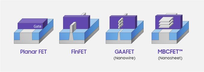
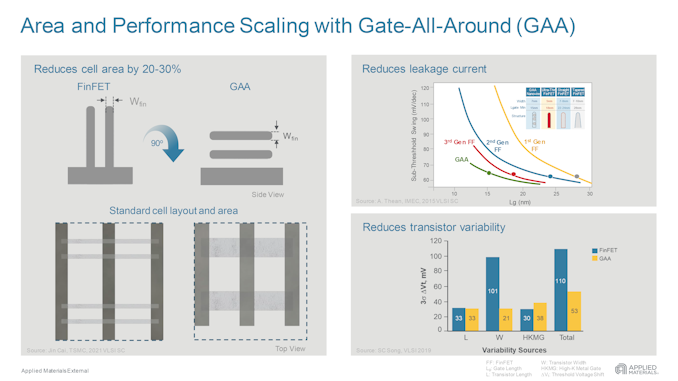
When TSMC first talked about its N2 in August 2020, it did not reveal many details about the technology (by now we know that it adopts gate-all-around [GAA] transistor structure) or its schedule, but indicated that it would build a brand-new fab near Baoshan, Hsinchu County, Taiwan, for this node (some sources call this new facility Fab 20). Taiwanese authorities approved the construction plan in mid-2021 and that plan included breaking ground in early 2022 (earlier this year TSMC’s board of directors indeed accepted capital appropriations for a new fab construction), so we believe that the shell is being built as we speak. 


Shell construction usually takes a year or a little more, then equipment installation takes over a year as well, so we expect the first phase of Fab 20 to be ready by mid-2024 at the latest. TSMC expects to start risk production using its N2 technology in late 2024 and then initiate HVM towards the end of 2025, which means that the gap between the initial N3 ramp in Q3 2022 and initial N2 ramp in Q4 2025 will be about three years.


“Our progress so far today for the N2 is on track,” said Mr. Wei. “All I want to say is, yes, at the end of 2024, [N2] will enter the risk production. 2025, it will be in production, probably close to the second half or the – or the end of 2025. That is our schedule.”


Considering how long modern chip production cycles are, it is safe to say that the first N2 chips made by TSMC will arrive in consumer devices no sooner than early 2026.


TSMC’s New Node Introduction in Recent Years
  N7 N7P N5 N5P N3 N3E N2
Transistor Type FinFET FinFET FinFET FinFET FinFET FinFET GAA FET
Risc Production ? ? ? ? 2021 2022 Late 2024
Volume

Manufacturing
Q2 2018

 
Q2 2019 Q2 2020

 
Q2 2021 Q3 2022 Q2/Q3 2023 Late 2025


But perhaps TSMC’s public disclosures about N2 and Fab 20 are too conservative. Analysts from China Renaissance Securities seem to be more optimistic about Fab 20 readiness than TSMC is, which may be an indicator that the foundry could pull-in N2 HVM by a quarter or even two if the fabrication process meets its performance, power, and yield goals.


“We also see more clarity around TSMC’s N2 expansion schedule in Fab 20 (Hsinchu),” Sze Ho Ng, an analyst with China Renaissance Securities, wrote in a report for clients. “Tool move-in is expected to start by end-2022, based on company plans, ahead of risk production in late 2024E with Intel (client PC Lunar Lake’s graphic ’tiles’, while the CPU ’tiles’ are fabbed using Intel’s 18A) and Apple being the anchor customers for dedicated capacity support.”


Meanwhile, pulling in a node from Q4 2025 to Q3 2025 when alpha customers already set their plans for 2025 may not make a lot of sense, but we will certainly see how things work out with N2.


More N3 Iterations


This year, TSMC’s customers that need a leading-edge fabrication process will use the company’s N4 technology, which belongs to the N5 family (along with N5, N5P, N4P, and N4X). Essentially, this means that an N5 node will remain TSMC’s most advanced offering for three consecutive years.


N3 nodes will also have to serve TSMC’s clients for another three years (2023, 2024, 2025), so we are going to see several iterations of this process. So far, TSMC has formally confirmed N3E and N3X (which is another performance-oriented manufacturing technology akin to N4X aimed primarily at CPUs and datacenter ASICs), but I would expect more N3-derived nodes to come to address mainstream SoCs in 2024 ~ 2025. 


Keeping in mind that TSMC’s FinFET-based N3 will have to stay competitive against GAA-based Samsung’s 3GAP and 2GAE/2GAP in 2023 ~ 2025 and Intel’s 20A (RibbonFET + PowerVia) in 2024 and 18A (High-NA EUV) in 2025, TSMC’s engineers will have to be quite creative with their N3 enhancements. 


On the foundry side of things, TSMC will remain ahead of its rivals for quite a while since Intel is not expected to invest significantly in its IFS-dedicated capacity before 2025 (so its 20A and 18A capacities for IFS customers will likely be limited), whereas Samsung Foundry is traditionally behind TSMC when it comes leading-edge capacity and prefers to prioritize its parent company and strategic clients (e.g., Qualcomm). But formal process technology leadership is what TSMC’s engineers will have to maintain with N3 and it will be uneasy to do considering how aggressive Intel and Samsung are.


Changes Are Coming


Evidently, TSMC’s brand-new process development and ramp up cadence has increased to two-and-a-half years with N3 and will increase to three years with N2, which may be considered as a major slowdown by its key customers. Meanwhile, potential pull-in of N3E is a good sign which shows that the company can make its intra-node advancements fairly quickly. Hence, the main question is how significant will TSMC’s intra-node advancements be going forward. This is a question that only time will answer.


In the meantime, it looks like with TSMC’s three-year new node development cycle, future intra-node advancements will be significantly more important for the company and its clients than they are today.


Source: AnandTech – TSMC Roadmap Update: N3E in 2024, N2 in 2026, Major Changes Incoming

The Vertiv Edge Lithium-Ion 1500 VA UPS Review: Impeccable Power, Imposing Price

Today we are having our first contact with Vertiv, a giant on power and cooling solutions for industrial IT infrastructure. Vertiv is taking a step into the top-tier retail market with their new UPS series, the Edge Lithium-Ion. Does it pose a threat to established manufacturers, such as APC, Eaton, and Cyberpower? We find out in this review.


Source: AnandTech – The Vertiv Edge Lithium-Ion 1500 VA UPS Review: Impeccable Power, Imposing Price

The FSP Hydro PTM Pro 1200W PSU Review: Improving on the Tried and True

Today we are having a look at one of the best PSUs FSP has to offer, the Hydro PTM Pro 1200W. FSP is an OEM who usually builds PSU platforms for other companies, however the Hydro PTM Pro is a PSU that they design and produce themselves, making it interesting to see what the company has to offer directly to the retail market.


Source: AnandTech – The FSP Hydro PTM Pro 1200W PSU Review: Improving on the Tried and True