NZXT Announce N7 and N5 Z690 Motherboards for Intel 12th Gen Core Processors

NZXT has announced a pair of new motherboards designed for Intel’s 12th Gen Core processors: the N7 Z690 and N5 Z690. The N7 Z690 positions itself as the premium model of the pairing and comes with armor covering the vast majority of the PCB, Wi-Fi 6E, and support for memory speeds up to DDR4-4800. The N5 Z690 opts for a less aggressive approach at a more affordable price but still comes with Wi-Fi 6E and supports all of Intel’s Alder Lake Core processors.


Starting with the most premium of NZXT’s new motherboard pairing for Intel’s 12th Gen family of processors, the NZXT N7 Z690 follows a similar design to previous iterations of its N series models, including the N7 Z490 which we previously reviewed. As with previous N series models from NZXT, these are designed around its range of chassis, such as the H series models, for a seamless look and design. Perhaps the most prominent feature of the N7 Z690 is that it has armor plating covering practically all of the PCB for a cleaner and sleeker look.


There’s space underneath the sleek armor for up to three PCIe 4.0 x4 M.2 drives and four SATA ports for conventional HDDs and optical media drives. NZXT includes one full-length PCIe 5.0 x16 slot, with the second full-length slot operating at PCIe 4.0 x4 and the bottom full-length slot operating at PCIe 3.0 x4. Inbetween the full-length slots are two PCIe 3.0 x1 slots, while the N7 Z690 includes support for DDR4 memory at speeds up to DDR4-4800, with four slots supporting up to 128 GB in total. 


The NZXT N7 Z690 is available in both black and white and includes a mid-range feature controller set with a Realtek RTL8125BG 2.5 GbE controller, an Intel AX210 Wi-Fi 6E CNVi, and a Realtek ALC1220 HD audio codec.


The NZXT N5 Z690 is the more affordable of the pair and doesn’t include all of the armor of the N7; instead, opting for a more barebone look that users are accustomed to with entry-level motherboards. It does have the same networking configuration as the N7 (RTL8125BG 2.5 GbE and AX210 Wi-Fi 6E), but it uses a cheaper and lower grade Realtek ALC897 HD audio codec, as well as support for DDR4 memroy up to DDR4-5000 speeds.


It has the same PCIe configuration as the N7 with one full-length PCIe 5.0 x16, one full-length PCIe 4.0 x4, one full-length PCIe 3.0 x4, and two PCIe 3.0 x1 slots. The N5 Z690 even includes four PCIe 4.0 x2 M.2 slots which is one more than the more expensive N7 Z690 model.


The NZXT N7 Z690 is available in black or white and can be purchased now directly from NZXT for $300. Without all the armor and a lower grade HD audio codec, the NZXT N5 Z690 is also available in black or white and can be bought from NZXT directly for $240.


Source: NZXT


Source: AnandTech – NZXT Announce N7 and N5 Z690 Motherboards for Intel 12th Gen Core Processors

Intel Unveils Rialto Bridge: Second-Gen Xe-HPC Accelerator to Succeed Ponte Vecchio

With ISC High Performance 2022 taking place this week in Hamburg, Germany, Intel is using the first in-person version of the event in 3 years to offer an update to the state of their high performance/supercomputer silicon plans. The big news out of the show this year is that Intel is naming the successor to the Ponte Vecchio accelerator, which the company is now disclosing as Rialto Bridge.

Previously appearing on Intel’s roadmaps as “Ponte Vecchio Next”, Intel’s GPU teams have been pipelining the development of Ponte’s successor even as the first large installation of Ponte itself (the Aurora Supercomputer) is still being stood up. As part of the company’s 3 year (ish) roadmap that leads to CPUs and accelerators converging with the Falcon Shores XPU, Rialto Bridge is the part that will, if you’ll pardon the pun, bridge the gap between Ponte and Falcon, offering an evolution of Ponte’s design that’s making use of newer technologies and manufacturing processes.


Source: AnandTech – Intel Unveils Rialto Bridge: Second-Gen Xe-HPC Accelerator to Succeed Ponte Vecchio

Intel Showcases Sapphire Rapids Plus HBM Xeon Performance at ISC 2022

Alongside today’s disclosure of the Rialto Bridge accelerator, Intel is also using this week’s ISC event to deliver a brief update on Sapphire Rapids, the company’s next-generation Xeon CPU which is shipping later this year. While Intel has been beating the drum for their forthcoming, 4th Generation Xeon Scalable chip for a while, we have yet to hear anything of significance about its expected performance – particularly in the HPC space. So ahead of its formal launch a bit later this year, Intel is finally talking a bit about the expected performance of the HBM-equipped version of the chip, which is aimed in particular at the HPC/supercomputing crowd.


Intel’s first tiled Xeon processor, Sapphire Rapids is also Intel’s first CPU to offer optional on-chip HBM memory, which is being dubbed Sapphire Rapids Plus HBM. The addition of 64GB of HBM2e makes it a fairly complex and expensive chip, but also one with access to far more memory bandwidth than any x86 CPU before it. As a result, the chip is of particular interest to a subset of the high-performance compute community, as it offers an alternative route for workloads that aren’t suitable for GPUs, but still need access to vast amounts of memory bandwidth.


As part of their ISC presentation today, Intel is releasing two slides with performance figures for the HBM version of Sapphire Rapids (Sapphire Rapids Plus HBM). The idea here is to show off the combination of architecture improvements – and in particular, the dedicated accelerator blocks – combined with using 64GB of HBM2e memory to keep those blocks well fed. The pre-production processors are being compared to Intel’s Xeon Platinum 8380 (Ice Lake-SP) chips.


Bearing in mind that these are going to be cherry-picked performance figures, Intel is seeing anywhere between a 2x speed-up in things like the WRF weather forecasting model, to over a 3x improvement for the CloverLeaf Euler equation solver. Both of which are somewhat narrow use cases, but important ones for the HPC market segment.


Sapphire Rapids Plus HBM is due to be released alongside the rest of the Sapphire Rapids family later this year. According to Intel’s current roadmaps, it is due for a successor in the 2023 timeframe, before the entire HBM-equipped Xeon lineup is due to be rolled into the Falcon Shores XPU in 2024.


Source: AnandTech – Intel Showcases Sapphire Rapids Plus HBM Xeon Performance at ISC 2022

AMD Corrects Socket AM5 Power Specifications: 170W TDP and 230W PPT

At Computex 2022, the CEO of AMD, Dr. Lisa Sui, unveiled its Ryzen 7000 series of processors, as well as the associated AM5 platform. But while discussing specific details about its new platform for Zen 4 and beyond, AMD inadvertently ended up creating a conflux of confusion around the AM5 platform by quoting different power figures to different groups. Ultimately, at different points AMD was quoting 170 Watts as both the highest nominal TDP supported by the platform, as well as the Power Package Tracking (PPT) rating, which is the absolute highest amount of power a chip can draw under load. It goes without saying that these two claims shouldn’t both be right, and a correction was needed.


As first reported by the Tom’s Hardware crew, AMD has published a statement addressing the confusion, and proving the correct values. In short, the 170 Watt TDP was correct. Meanwhile the PPT value is actually 230 Watts – which at 1.35x the TDP rating, is typical for AMD’s Ryzen processors.


AMD’s full statement is below:


AMD would like to issue a correction to the socket power and TDP limits of the upcoming AMD Socket AM5. AMD Socket AM5 supports up to a 170W TDP with a PPT of up to 230W. TDP*1.35 is the standard calculation for TDP v. PPT for AMD sockets in the “Zen” era, and the new 170W TDP group is no exception (170*1.35=229.5). 


This new TDP group will enable considerably more compute performance for high core count CPUs in heavy compute workloads, which will sit alongside the 65W and 105W TDP groups that Ryzen is known for today. AMD takes great pride in providing the enthusiast community with transparent and forthright product capabilities, and we want to take this opportunity to apologize for our error and any subsequent confusion we may have caused on this topic.


The overall increase in power specification figures for the AM5 platform was not unexpected – part of the benefit of the move to LGA sockets is additional pins for power delivery – but this finally settles the matter of just how much power AMD’s new socket and platform are designed to deliver. Motherboard vendors will no doubt go (well) past this on their high-end boards, of course, but 170W/230W will be the baseline for any motherboard that wants to officially support high-end AM5 chips.


CPU power consumption has been on the rise for the past several years, as we’re now well into the Dark Silicon era. While an individual CPU core still only draws a modest amount of power – on the order of 20W to 30W for a high-performance core – the total power requirement quickly balloons for high-end processors, which pack upwards of 16 cores. As a result, power delivery limits are typically the constraining factor for heavily multi-threaded workloads, as CPUs have to back down on clockspeeds in order to stay within their power envelopes. Increasing platform power limits, in turn, offers more headroom for keeping more cores clocked higher more often.


Though it should be noted that AMD’s clarifications today are for the AM5 socket, not the initial Ryzen 7000 series chips that will use it. AMD doesn’t necessarily have to tap into the full TDP of the socket right away – though for the aforementioned MT performance reasons, there’s good reason to. So officially, we still don’t know what the TDPs of the high-end Ryzen 7000 processors will be; but unofficially, it wouldn’t be surprising to see the top chips approach 170 Watts.


Finally, it would seem that we should expect to see the Ryzen 7000 family hit that full TDP out of the gate. According to a comment from an AMD spokesperson on Reddit, the top TDP of the Ryzen 7000 series will indeed be 170 Watts, with PPTs reaching 230 Watts.


Source: AnandTech – AMD Corrects Socket AM5 Power Specifications: 170W TDP and 230W PPT

Computex 2022: TeamGroup Announces T-Force Delta RGB DDR5-6600 CL34 and DDR5-6000 CL30 Memory

Memory vendor TeamGroup has announced two new T-Force Delta RGB DDR5 memory kits during Computex 2022, being held in Taipei, Taiwan. This includes a high-frequency kit clocked to DDR5-6600 with a latency of CL34, as well as a low-latency kit operating at DDR5-6000 CL30. Both will be available in black or white and come with RGB LEDs.


Intel was the first company to introduce DDR5 memory to the desktop market in November 2021 with its 12th Gen Core series of processors. During its keynote at Computex, AMD announced that its latest Ryzen 7000 processors, due in the fall, will also support DDR5 memory, among many other interesting features. We did test how well DDR5 memory scales on Intel’s 12th Gen Alder Lake platform, and there is merit to using both high-frequency and low latencies to maximize performance.


TeamGroup intends to add two new speed grades of its T-Force Delta RGB DDR5 memory, one with DDR5-6600 CL34 specifications and one with DDR5-6000 CL30. Both variants will be available in 32 GB kits (2 x 16 GB), with options including a striking white or subtle black heatsink. Both color schemes include an RGB-enabled lightbar with a 120° angle with smart RGB customization control. TeamGroup states that it uses carefully selected memory ICs, but they don’t specify which manufacturer’s DRAM the kits will be using.


The TeamGroup T-Force Delta RGB DDR5-6600 CL34 and DDR5-6000 CL30 are expected to hit retail shelves in July, but we currently don’t have any details on pricing.


Source: TeamGroup


Source: AnandTech – Computex 2022: TeamGroup Announces T-Force Delta RGB DDR5-6600 CL34 and DDR5-6000 CL30 Memory

ASML High-NA Development Update: Coming to Fabs in 2024 – 2025

It took the semiconductor industry over a decade to prep everything needed for production of chips using extreme ultraviolet (EUV) lithography. It looks like it is going to take a lot less to reach the next level — EUV with High-NA.


Higher Resolution Needed


Nowadays the most advanced chips are made on 5/4-nm-class process using EUV lithography ASML’s Twinscan NXE:3400C (and similar) systems that feature a 0.33 numerical aperture (NA) optics, which provides a 13 nm resolution. This resolution is good enough for a single-pattern approach at 7 nm/6 nm nodes with 36 nm ~ 38 nm pitches and at 5nm with 30 nm ~ 32 nm pitches. But as pitches get below 30 nm (at beyond 5 nm nodes) the 13 nm resolution might call for dual lithographic exposure that is going to be used for years to come. 


For post-3nm nodes, ASML and its partners are working on a brand-new EUV tool — the Twinscan EXE:5000-series — featuring a 0.55 NA (High-NA) lens capable of an 8nm resolution, which is projected to avoid multipatterning at 3 nm and beyond. The new High-NA scanners are still in development, they are expected to be extremely complex, very large, and expensive — each of them will cost over $400 million. High-NA will require not only new optics, but a new light source too, and even new fab buildings to accomodate the larger machines, which will require major investments.


But in a bid to keep scaling performance, power, area, and costs (PPAc) of semiconductors, leading makers of logic chips and memory devices are willing to adopt new technologies, and High-NA EUV scanners are crucially important for post 3-nm nodes. As a result, demand for High-NA tools is, well, pretty high. 


10 to 20 High-NA Systems to Be Delivered


Several weeks ago, ASML disclosed that it had received multiple orders in Q1 2022 for its High-NA Twinscan EXE:5200 systems (EUV 0.55 NA) from both logic and DRAM customers. Last week it clarified that it had five orders for pilot High-NA scanners due to be delivered in 2024 and ‘over five’ orders for subsequent models featuring higher productivity that will be delivered starting from 2025, reports Reuters.


Interestingly, back in 2020 ~ 2021, ASML said that it had has received High-NA commitments from three customers, for a total of up to 12 systems. Keeping in mind that logic makers are usually the first to adopt leading edge tools, it is safe to bet that Intel, Samsung Foundry, and TSMC committed in 2020 ~ 2021 to get pre-production High-NA scanners. Moreover, ASML has already started building the first High-NA system, which will be completed in 2023 and will be used by Imec and ASML customers for research and development purposes.


“On High-NA EUV, we are making good progress and have currently started the integration of the first High-NA system in our new cleanroom in Veldhoven,” said Peter Wennink, chief executive of ASML. “We received multiple orders for our EXE:5200 system in Q1. We also received additional EXE:5200 orders this month, April. With these bookings, we now have High-NA orders from three Logic and two Memory customers. The EXE:5200 is ASML’s next model High-NA system and will provide the next step for lithography performance and productivity.”


ASML’s Twinscan EXE:5200 is considerably more complex than regular Twinscan NXE:3400C machines, so it takes longer time to build these tools. The company hopes that it will be able to deliver as many as 20 High-NA systems in mid-term future, which probably means that its customers will have to compete for these machines.


“We are also discussing with our supply chain partners to secure a capacity of around 20 EUV 0.55NA systems in the medium term,” said Wennink. 


Intel First to Adopt Pre-Production Tools


So far, the only process technology confirmed to use ASML’s High-NA tools is Intel’s 18A node and that one was once scheduled to enter high-volume production in 2025, around the time when ASML starts to deliver its production High-NA EUV systems. But recently Intel pulled-in the start of18A production to the second half of 2024 and indicated that it could use ASML’s Twinscan NXE:3600D or NXE:3800E for its 18A manufacturing, presumably via multi-patterning.


While Intel’s 18A technology would greatly benefit from High-NA EUV tools, it looks like Intel does not necessarily need Twinscan EXE:5200 machines for this node. Usage of multi-patterning for commercial chips means a longer product cycle, lower productivity, higher risks, and potentially lower yields (though the latter is not cast in stone). Yet, it looks like Intel wants its 18A node to arrive as soon as possible, perhaps because it considers it a major tool that will allow it to recapture process technology leadership from TSMC. Consequently, Intel’s updated plans are now to phase in High-NA tooling during 18A’s lifecycle if the tools are completed on time.


Of course, it remains to be seen whether usage of 0.33 NA EUV scanners for 18A will offer enough productivity for Intel and customers of Intel Foundry Services. But, at least in 2024, Intel is not going to have any choice but to use machines that it has.


Other leading makers of semiconductors — TSMC, Samsung, SK Hynix, and Micron — will also inevitably adopt High-NA EUV for high-volume manufacturing of chips. The only question is when exactly this is when exactly this is set to happen. 


Source: AnandTech – ASML High-NA Development Update: Coming to Fabs in 2024 – 2025

Computex 2022: ASRock Unveils X670E Taichi and Taichi Carrara Edition Motherboards

At Computex 2022 in Taipei, Taiwan, ASRock has lifted the lid on a few of its X670E motherboards designed for AMD’s upcoming Ryzen 7000 series of processors. The first two of ASRock’s socket AM5 motherboards include the X670E Taichi and the special edition X670E Taichi Cararra. While both X670E Taichi boards are aesthetically different, the two share the same core feature set, including support for PCIe 5.0, DDR5 memory, and dual Thunderbolt 4-enabled USB Type-C ports on the rear panel.


The ASRock Taichi series is one of the most popular and premium models in its line-up. For years, the Taichi aesthetic has brought cogwheels to the design, and the Z590 Taichi for Intel’s 11th Gen Core series even included a motorized cogwheel integrated into the rear panel cover.


The only difference between the ASRock X670E Taichi and the X670E Taichi Cararra is the design. The regular X670E Taichi has a primarily black finish with a bronze-looking trim on the left-hand side of the board, with RGB LEDs built into the chipset heatsink.


ASRock X670E Taichi (left) and X670E Taichi Cararra (right) motherboards


The X670E Taichi Cararra is based on Cararra Marble from Italy, which is white in color and was used for many years in ancient Roman architecture due to its elegance and strength. It is designed to celebrate the 20th anniversary of ASRock, and ASRock hasn’t specified if the Cararra edition will be limited in numbers like its Aqua series or if it will cost more than the regular X670E Taichi.


In terms of features, both ASRock X670E Taichi models boast an advertised 26-phase power delivery, which is mightily impressive. Other features include support for DDR5 memory, dual full-length PCIe 5.0 slots (x16, x8/x8), and one PCIe 5.0 x4 M.2 slot, three PCIe 4.0 x4 M.2 slots, and eight SATA ports.


A Realtek ALC4082 HD audio codec and ESS Sabre ES9218 DAC power the onboard audio solution on the rear panel, while a Killer E3100G 2.5 GbE controller and Killer AX1675 Wi-Fi 6E provide solid networking connectivity. Regarding connectivity, ASRock includes dual Thunderbolt 4 Type-C ports, five USB 3.2 G2 Type-A, and three USB 3.2 G1 Type-A ports.


At present, ASRock hasn’t revealed pricing on the X670E Taichi and X670E Taichi Cararra Edition motherboards, but we expect to find out more closer to the launch of AMD’s Ryzen 7000 processors expected in the fall.


Source: ASRock


Source: AnandTech – Computex 2022: ASRock Unveils X670E Taichi and Taichi Carrara Edition Motherboards

Computex 2022: MediaTek Announces Wi-Fi 7 Access Point and Client Platforms

Mediatek was one of the first vendors to demonstrate working 802.11be-compliant silicon under the Filogic lineup in January 2022. As part of the announcements at this week’s Computex, the company provided additional technical details along with part numbers. The Filogic 880 platform will service access points, routers, and gateways, while the Filogic 380 will be seen in the client devices.


Wi-Fi 7 / 802.11be Background


The 802.11 Working Group focused on extremely high throughput when starting work on 802.11be. This has been achieved primarily through a combination of three different aspects:


  • Support for up to 16 spatial streams
  • Support for channel widths up to 320MHz (with operation in 2.4 GHz, 5 GHz, and 6 GHz bands)
  • Support for 4096-QAM (4K-QAM) resulting in better utilization of available spectrum (a faster modulation / coding scheme).


It must be noted that wider channels are available only in the 5 GHz and 6 GHz bands. Theoretically, these aspects allow for up to around 46 Gbps of wireless throughput. 802.11be also aims to enable usage of Wi-Fi for real-time applications by including features for low-latency communications such as Multi-link operation (MLO). This allows a client and an access point to simultaneously communicate over multiple channels that might even belong to different bands.


Source: Mediatek Wi-Fi 7 Whitepaper


802.11ax introduced OFDMA to split the channel into multiple resource units (RUs), allowing multiple clients to receive data packets simultaneously. Wi-Fi 7 brings in a Multiple RU (MRU) feature that allows punctured RUs (at a 20 MHz granularity). Puncturing enables interference mitigation, and also increases the OFDMA efficiency.


Source: Mediatek Wi-Fi 7 Whitepaper


The benefits of MRU are brought out in the above picture – on top, puncturing allows improvement in spectral efficiency, and hence, data bandwidth. Below that, we see obvious latency benefits when multiple clients are simultaneously active.


Interference and co-existence with non-Wi-Fi users of the same spectrum is handled using automatic frequency coordination (AFC). While Broadcom’s pledge of support for the Open AFC initiative, and Qualcomm providing its own turnkey solution for its customers, Mediatek has only indicated that the Filogic 880 platform supports AFC, with no additional details.


Mediatek Filogic 880 Platform


Mediatek’s Filogic 880 platform services the Wi-Fi 7 access point and wireless router market. Similar to its competitor’s offerings, the platform supports all the major Wi-Fi 7 features – 320 MHz bandwidth in the 6GHz band, 4K-QAM, Multi-link operation (MLO), Automatic Frequency Coordination (AFC), and Multiple Resource Units.


The platform supports up to five bands with independent RFICs that communicate with the Filogic 680 Wi-Fi 7 baseband chip. While traditional routers may use only three bands, mesh systems and premium routers can make use of the support for two additional bands. At the heart of the reference design is a 1.8 GHz quad-core Cortex A73-based WiSoC. It also includes a network processing unit (NPU) with hardware-accelerated QoS and tunneling offload engines. The WiSoC doesn’t include an integrated switch, though. Designs are expected to adopt an external switch to translate one of the two 10Gbps USXGMII ports to either a single 10GbE, or a mix of NBASE-T and Gigabit Ethernet ports. Various other high-speed I/Os are also available in the WiSoC.


Unlike Qualcomm (whose announcement of the Wi-Fi 7 Networking Pro product suite was covered earlier this month), Mediatek is adopting an open approach in terms of making technical details of the platform available to the public. Broadcom also adopted a similar approach while introducing their product suite.


The Filogic 880 platform’s WiSoC is fabricated in a 6nm process. According to Mediatek, this delivers significant power efficiency compared to its competitors (without public knowledge of the fabrication process for Qualcomm’s and Broadcom’s offerings and/or public availability of their platforms, this claim is difficult to evaluate).


The MAC/baseband is implemented in the Filogic 680 part. Here, Mediatek opts for an interesting approach The 6GHz band also adopts a 4T5R (quad-transmit, penta-receive) antenna configuration to boost throughput and range, particularly for backhauls in mesh systems. The Filogic 680 contains the MAC and baseband logic for all three bands, and also includes MLO control. Mediatek contends that this approach is better than the scheme of discrete MAC/PHYs for each band between the WiSoC and the basebad/RFIC, and putting the MLO logic in the WiSoC – in terms of latency (claims of up to 100x improvement) as well as board design cost.


Mediatek’s reference design is a four-layer PCB, which should lead to a lower cost for its customers. Mediatek claims that the multi-chip MAC / PHY / baseband approach of its competitors results in higher cost due to more complex PCBs (six or eight layer PCBs). These aspects should be readily evident to end users when routers / APs based on platforms from different vendors come to the market.


Mediatek Filogic 380


On the client side, Mediatek is announcing the Filogic 380 combo solution with support for Wi-Fi 7 and Bluetooth 5.3. This combo single-chip solution is also built on a 6nm process. The 2×2 solution supports speeds up to 6.5Gbps with dual-band dual-concurrent operation. 320 Mhz bandwidth, 4K-QAM, MLO, and MRU are supported.


Mediatek also indicated support for an extra receive antenna to improve performance and range for Bluetooth 5.3 connectivity by enabling MRC (multiple receive combining). Bluetooth LE audio is also supported. The Filogic 380 also includes coexistence technology to ensure that BT and Wi-Fi can both operate in the 2.4GHz band without interference. Host connectivity is either via PCIe 4.0 x1 or USB 3.0.


Mediatek is currently demonstrating both platforms at Computex 2022. Based on Mediatek’s claims, it appears that routers and APs based on the Filogic 880 should hit very attractive price points without sacrificing anything in terms of performance or  features. Products based on the new Filogic platforms should start appearing in the market within a few quarters.


Source: AnandTech – Computex 2022: MediaTek Announces Wi-Fi 7 Access Point and Client Platforms

Sponsored Post: Comino Grando RM Multi-GPU Workstations Offer Unmatched Performance and Quality

Comino Grando RM workstations are a new breed of Hyper Performance workstation (HYPE WS) that can transform the workflows of creatives, scientists and medical researchers who rely on artificial intelligence and machine learning.


If your work is dependent on some serious GPU horsepower, Comino Grando RM workstations offer a solution that isn’t just extremely powerful – but also incredibly quiet. This is thanks to their server-grade liquid cooling, which keeps the temperature of the components down, even when working hard. Rather than using noisy fans, which can get distracting, water cooling is more efficient, and crucially, a lot quieter.


Comino Grando RM workstations are built to order in the EU, maintaining the highest possible build quality, and thanks to a range of unique configuration options, you can order one that perfectly suits your needs.


Built to Last


Comino’s motto is “engineered, not assembled”, and each workstation has been designed from the ground-up to provide maximum performance and build quality.


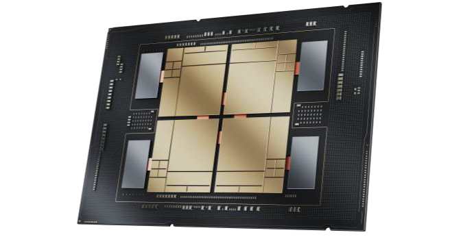
Almost every aspect of these workstations are designed and built by Comino, with over 90% of the components designed by the company itself. This level of detail and control allows each part of the workstation to work as one, delivering unrivalled performance and reliability.


The unique liquid cooling loop in every workstation is controlled and monitored by a controller built by Comino, which uses numerous sensors to keep track of the system’s health and performance. Thanks to Comino Monitoring Software, you can also check your system’s health remotely, for complete peace of mind.


The flexibility of Comino Grando RM workstations doesn’t just stop at unique configurations, but also how you buy. You can purchase Comino Grando RM workstations outright, but for UK customers there are also options to lease them as well.


Handling Everything You Need


Thanks to the raw power of Comino Grando RM workstations, they can cover almost all of your inhouse computation tasks, and you’ll rarely need to rely on cloud services to help finish your projects.


Even better, if you have several Comino Grando RM workstations, they can be used to create your very own cloud, allowing you to access the power of these Hyper Performance workstations remotely – perfectly fitting in with our new hybrid way of working.


Because they are so silent when in use, you can use them in an office or studio, or you can install them in a server rack. When installed in a server rack, they can use external cooling for even more impressive performance, supporting up to seven GPUs per system. This method can also be environmentally friendly, as the heat dispelled by Comino Grando RM systems can be repurposed to heat living and office spaces.


Packing hardware like four Nvidia RTX A100 80GB GPUs plus AMD Threadripper Pro, dual Intel Xeon 8368Qs, or dual EPYC CPUs, air cooling solutions would struggle to keep these components cool without producing a lot of noise.


With server-grade liquid cooling, AI research teams, for example, can use the workstations without being distracted by the whirring of fans. Meanwhile, medical teams working in highly controlled environments will appreciate the slower airflow produced by liquid cooling, as well as reduced dust collection.


So, it’s no surprise that Comino Grando RM workstations have been embraced by companies around the world, and used in projects such as the Flamemapper in California, which uses Comino Grando RM Multi-GPU workstations to help predict the effect of wildfires on structures, and can help emergency planners to place protective measure where they are needed the most.


Many CG and 3D rendering studios rely on Comino Grando RM Multi-GPU workstations to create complex and realistic models and scenes.


Danil Krivoruchko, a renowned digital artist based in New York, and who works with the likes of Apple, Nike and Boeing, explains how Comino Grando RM workstations have helped him with his work.


“I’ve used numerous Comino Grando RM workstations during my work on the breakthrough user-influenced self-evolving NFT project, Organic Growth: Crystal Reef, which combines generative art, blockchain, NFTs and user interaction. This project is so unique, multi-layered and complex both visually and computationally, that we had to hire the whole render farm, packed with Grando RMs by Comino, for 3 months to support its development. I got the workstation for myself, as well, to progress through the project faster, as it’s hard to find another workstation as versatile and quiet as Grando RM.”


Successful AI artist and NFT enthusiast from New Zealand, Jesse Woolston, also relies on Comino’s workstations.


“My approach is to use the Comino Grando RM for all my modeling and simulation. So I use it for production, then I have a small render farm to utilize GPU alongside the Comino.


My work focuses on using AI & physics modeling as a means to re-contextualize how we see nature. So far, I’ve been able to use the Comino Grando RM in multiple circumstances from training my own models to simulating the oceans. The machine has been working beautifully in both large and small scales.


The main factor as to why I love the Comino Grando RM is its ability to be diverse with training and modeling, where I can give it any and all assignments.


I don’t have to think too deeply about how to adapt the work to fit my tools, I am able to just utilize the tools and focus on the art.”


Influencers such as sentdex and LEDunit have also been blown away by the possibilities of Comino Grando RM workstations.


If it sounds like  Comino Grando RM workstations would be perfect for your projects, then head over to Comino’s Grando website to find out more.


Source: AnandTech – Sponsored Post: Comino Grando RM Multi-GPU Workstations Offer Unmatched Performance and Quality

Computex 2022: ASUS Announces ROG Swift 500 Hz G-Sync Gaming Monitor

In direct collaboration with NVIDIA, ASUS has announced the world’s first 500 Hz G-Sync enabled gaming display during Computex 2022. The latest ROG Swift 24.1-inch display will feature a 500 Hz panel with a 1080p resolution and comes loaded with features such as NVIDA’s Reflex Analyzer and a new vibrance mode.


Designed more the fast-paced eSports titles such as Counter-Strike: Global Offensive, Valorant, Overwatch, and titles like these, the latest monitor from ASUS’s premium ROG Swift range now features an impressive 500 Hz E-TN display. Not to be confused with the standard TN panels, ASUS uses its new “eSport TN” technology, which ASUS claims offers 60% better response times.


In the above video embedded, ASUS and NVIDIA give a small demonstration of the benefits of moving to 500 Hz from 240 and 144 Hz. It tests things such as animation smoothness, ghosting, and system latency.


The ASUS ROG Swift 500Hz uses a 24.1-inch panel with a 1080p resolution. It also benefits from NVIDIA G-Sync and NVIDIA’s Reflex Analyzer, which is designed to detect system latency, measure mouse clicks when using an NVIDIA Reflex certified gaming mouse, and to measure the time for the resulting pixels to change on the screen.


ASUS also includes a new enhanced vibrance mode, which is specifically tuned for eSports and is built into the monitor’s firmware. ASUS claims this allows light to travel through the LCD crystals for better color vibrancy.


As we’ve seen from previous ROG Swift releases over the years, don’t expect this to be cheap or affordable for the everyday gamer. At the time of writing, ASUS hasn’t revealed the expected MSRP of the ROG Swift 500 Hz gaming monitor, nor does it state when it might hit retail shelves.


Source: ASUS


Source: AnandTech – Computex 2022: ASUS Announces ROG Swift 500 Hz G-Sync Gaming Monitor

Computex 2022: MSI Announces Three AM5 Motherboards For Ryzen 7000 Processors

During Computex 2022 in Taipei, Taiwan, MSI unveiled four AM5 motherboards designed for AMD’s Ryzen 7000 processors, which will be landing later this year. Currently announced are the premium MEG X670E Ace, the mid-ranged MPG X670E Carbon WIFI, and the more business-focused Pro X670-P WIFI motherboards.


Hot on the heels of AMD’s announcement that its highly anticipated Ryzen 7000 processors for desktops will be dropping sometime in the fall, motherboard vendors have been slowly unveiling what boards we can expect to see at launch. MSI has dropped some limited information on four new AM5 boards, including two from its flagship MEG series, one from its gaming-focused MPG family, and one from its more affordable Pro series.


Here is what we know so far:


Although MSI has announced there will be an X670E Godlike, we currently don’t have any images for this model. As we know from previous motherboard launches, the MSI X670E Godlike will be the company’s flagship AM5 board for Ryzen 7000 processors, with a large E-ATX sized PCB and a wave of high-end enthusiast-level features. One interesting feature of the MEG series boards is a front panel USB 3.2 G2x2 Type-C header with support for 60 W power delivery.


MSI hasn’t specified much or distinguished much of its announced features between either model. Still, MSI does say the MEG series for AM5 includes a monstrous 26-phase power delivery (24+2) with 105 A smart power stages and a stacked fin array heatsink to help cool it. MSI also states that the MEG series will include a large metal backplate with up to four M.2 slots onboard and an M.2 Xpander-Z Gen5 dual add-on card supporting two PCIe 5.0 M.2 SSDs. Whether these features are specific to the entire MEG series for AM5 remains to be seen. 


The MSI MPG X670E Carbon WIFI uses a carbon black finish across the board, with two full-length PCIe 5.0 slots. MSI states the X670E Carbon WIFI will include four PCIe 5.0 M.2 slots and that the board will be powered by a 20-phase (18+2) power delivery with 90 A power stages.


MSI’s fourth and final model is the Pro X670-P WIFI motherboard, which is primarily aimed at SMEs and users looking to build a more professional type system. MSI says the X670-P WIFI will include a 16-phase (14+2) power delivery, with a single PCIe 5.0 M.2 slot and 2.5 GbE/Wi-Fi 6E networking.


At the time of writing, MSI hasn’t provided any information regarding controller sets at this time, or how much each of the four models might cost. MSI will likely give more details closer to the launch of the AMD Ryzen 7000 CPUs, which are expected to hit retail shelves in Q4 2022.


Source: MSI


Source: AnandTech – Computex 2022: MSI Announces Three AM5 Motherboards For Ryzen 7000 Processors

Computex 2022: ASUS Unveils ROG Crosshair X670E Extreme Motherboard for Ryzen 7000

Following on from AMD’s official announcement during Computex 2022 that its highly anticipated Ryzen 7000 series of processors will land sometime in Q4 2022, ASUS has lifted the lid on its flagship AM5 motherboard. Based on AMD’s ‘Extreme’ X670 chipset variant, the ASUS ROG Crosshair X670E Extreme motherboard is fully loaded with many features, including PCIe 5.0, support for DDR5 memory, and large 22-phase power delivery for enthusiasts.


Designed to offer leading-edge performance for AMD’s Ryzen 7000 processors, the ASUS ROG Crosshair X670E Extreme, ASUS has gone all out with a premium controller set and a wide array of features for users to get the most out of the new AM5 socket. This includes a typical ASUS ROG design with plenty of RGB LED lighting and its latest Q-Design features designed to make installation as easy as possible. It also benefits from an AniMe Matrix 2 LED display and ASUS’s LiveDash OLED for maximum customizability. 


Q-Design includes new release buttons for the PCIe slots and right-angled connectors on the right-hand side of the board for better cable management.


The ROG Crosshair X670E Extreme’s main features include a large 22-phase (20+2) power delivery with premium 110 A power stages. At the same time, networking options consist of a Marvell AQtion 10 GbE controller, a secondary Intel 2.5 GbE controller, and Intel’s Wi-Fi 6E CNVi. For audio, ASUS uses a ROG SupremeFX ALC4082 HD audio codec with a premium ESS Sabre ES9218PQ DAC for ultra-low distortion. 


Although ASUS hasn’t revealed a complete list of specifications, we know the X670E Extreme will feature two full-length PCIe 5.0 slots operating at x16/x0 or x8/x8, with a smaller PCIe slot at the bottom. It also benefits from five M.2 slots, with two of these conforming to the latest PCIe 5.0 specification and adding USB4 ports and a USB 3.2 G2x2 Type-C front panel header for connectivity. ASUS also includes a ROG M.2 add-in card next to the four DDR5 memory slots, although we don’t know what type of drives these will support at the time of writing. 


As we previously mentioned, ASUS hasn’t unveiled the full specifications list of the ROG Crosshair X670E Extreme motherboard, nor how much it will cost. We expect ASUS to reveal more details as we head closer to AMD’s Ryzen 7000 launch, expected sometime in the fall of 2022. 


Source: ASUS


Source: AnandTech – Computex 2022: ASUS Unveils ROG Crosshair X670E Extreme Motherboard for Ryzen 7000

NVIDIA To Release Liquid Cooled A100 and H100 PCIe Accelerators

Among NVIDIA’s slate of announcements tonight at Computex 2022, the company has revealed that it is preparing to launch liquid cooled versions of their high-end PCIe accelerator cards. Being offered as an alterative to the traditional dual-slot air cooled cards, the liquid cooled cards come in a more compact single-slot form factor for both improved cooling and improved density. The liquid cooled A100 will be available in Q3, and a liquid cooled H100 will be available early next year.


While liquid cooling is far from new in the datacenter, it’s typically been reserved for more bespoke hardware with extreme cooling and/or density requirements, such as the upcoming generation of high-end NVIDIA H100 (SMX) servers. PCIe servers, by contrast, are all about standardization and compatibility. Which for server video cards/accelerators means dual slot cards designed for use with forced air cooling within a server chassis. This serves the market segment well, but the 300 to 350 Watt TDPs of these cards means that they can’t get any thinner and still be effectively cooled by air – which in turn creates a 4 card limit for standard rackmount systems.


But times are changing, and liquid cooling is being implemented in datacenters in greater capacities both to keep up with cooling ever-hotter hardware, and to improve overall datacenter energy efficiency. To that end, NVIDIA will be releasing liquid cooled versions of their A100 and H100 PCIe cards in order to give datacenter customers an easy and officially supported path to installing liquid cooled PCIe accelerators within their facilities.


The cards (pictured above) are essentially a reference A100/H100 with the traditional dual-slot heatsink replaced with a single-slot full coverage water block. Designed to be integrated by server vendors, they use an open loop design that is meant to be used as part of a larger liquid cooling setup.


But other than changing the cooling system, the specifications of the cards remain unchanged. NVIDIA isn’t increasing the TDPs or clockspeeds on these cards, so their performance should be identical to traditional air cooled cards (so long as they’re not thermally throttling, of course). Put another way, these new cards are using liquid cooling to improve energy efficiency and density, rather than performance.


The first card out of the gate will be the liquid cooled version of the 80GB A100 PCIe accelerator. That will be available to customers in Q3 of this year. Meanwhile a liquid cooled version of the H100 PCIe is also under development, and NVIDIA expects that to be available in early 2023.


In the interim, NVIDIA has been working with Equinix in order to qualify the liquid cooled A100 within their datacenters, as well as to get an idea of the real-world power savings of the new hardware. Interestingly, NVIDIA is reporting a significant reduction in overall datacenter power usage from switching to liquid cooling – a 2000 server (4000 A100 card) setup saw its total power needs drop by 28%. According to NVIDIA, this is from a combination of overall power savings across the datacenter from the switch, including everything from improved video card energy efficiency from lower temperatures, to reduced energy needs from cooling water versus running large air chillers. All of which underscores why NVIDIA is promoting liquid cooled hardware as a power efficiency gain for datacenter operators who are looking to trim power usage.


And while this first generation of liquid cooled hardware is focused on efficiency, according to NVIDIA that won’t always be the case. For future generations of cards the company will also be looking at liquid cooling to improve performance at current energy levels – presumably by investing the datacenter-scale gains back into higher TDPs for the cards.


Finally, while the bulk of NVIDIA’s announcement today (as well as the case study) is focused on PCIe cards, NVIDIA is also revealing that they’ve been working on official, liquid cooled designs for their HGX systems as well, which are used to house the company’s more powerful SMX cards. A liquid cooled HGX A100 is already shipping, and a liquid cooled HGX H100 is slated to be released in Q4.


Source: AnandTech – NVIDIA To Release Liquid Cooled A100 and H100 PCIe Accelerators

Computex 2022: NVIDIA Keynote Live Blog (11pm ET/03:00 UTC)

Kicking off day two of our Computex coverage is NVIDIA, who will be delivering an hour-long keynote for the show.

The untitled keynote is slated to run for an hour and features a who’s who of NVIDIA VPs, including Ian Buck (VP Accelerated Computing), Michael Kagan (CTO), and Jeff Fisher (SVP GeForce). So expect the varied presentation to cover everything from datacenters to gaming. Or, as NVIDIA puts it:

“AI on the NVIDIA accelerated computing platform is revolutionizing everything from gaming to data centers to robotics. NVIDIA will present how AI is powering the enterprise data center and the latest products and technologies for gamers and creators.”

So be sure to join us at 11pm Eastern (03:00 UTC) to see what NVIDIA has in store for its users big and small over the coming months.


Source: AnandTech – Computex 2022: NVIDIA Keynote Live Blog (11pm ET/03:00 UTC)

AMD Announces Mendocino APU: 6nm Mainstream Mobile Zen 2 Laptop Chip Coming In Q4

Alongside their big desktop update for later in the year, AMD is also using this year’s Computex to announce an update to the low-end segment of their mobile lineup. In the fourth quarter of this year the company will be rolling out a new chip codenamed “Mendocino”, which is aimed at mainstream, high-volume Windows and ChromeOS notebooks. With 4 Zen 2 cores and RDNA 2 graphics, the relatively petite chip is intended to go into notebooks in the $399 to $699 range.

Based on its intended market segment, AMD Mendocino (no relation to Intel’s) is positioned to end up as the successor to a mix of lower-end AMD SoC products, including the bottom of the Ryzen mobile stack (e.g. Ryzen 5300U) as well as AMD’s Ryzen C-class chips. Mainstream laptops are a huge part of the market in volume, and for both good reasons and bad, it’s always been an area where AMD has done well for itself. And while the current chip shortage hasn’t been fully resolved, AMD is finally in a position to update the lower-end of its APU lineup with some newer hardware built on a more recent manufacturing process, replacing their current hodgepodge of mostly Picasso (4C 12nm Zen+) based SKUs.


Source: AnandTech – AMD Announces Mendocino APU: 6nm Mainstream Mobile Zen 2 Laptop Chip Coming In Q4

AMD Ryzen 7000 Announced: 16 Cores of Zen 4, Plus PCIe 5 and DDR5 for Socket AM5, Coming This Fall

During the AMD Keynote at Computex 2022, its CEO, Dr. Lisa Su officially unveiled their next generation of Ryzen processors and the successor to the highly successful Ryzen 5000 series. The new family, the Ryzen 7000 series, will feature up to 16 Zen 4 cores using TSMC’s optimized 5 nm manufacturing process. 

AMD Ryzen 7000 also officially marks the end of its long-serving AM4 socket, with the new AM5 LGA1718 socket replacing it with a freshly announced trio of new performance-driven chipsets, including X670E, X670, and B650.


Source: AnandTech – AMD Ryzen 7000 Announced: 16 Cores of Zen 4, Plus PCIe 5 and DDR5 for Socket AM5, Coming This Fall

Computex 2022: AMD Live Blog Keynote (2am ET/06:00 UTC)

Although COVID isn’t over quite yet, things are close enough for this year’s Computex event. Kicking things off once again is AMD, who is broadcasting a keynote address headed up by the one and only Dr. Lisa Su.


According to AMD, the PC-focused keynote will cover both mobile and desktop, with AMD and its partners focusing on cutting edge hardware and “breakthrough performance.” AMD’s Computex keynotes rarely disappoint, and we don’t expect this one too, either.


So be sure to join us at 2am Eastern (06:00 UTC) to catch a glimpse of what AMD has planned for the rest of 2022 and beyond.


Source: AnandTech – Computex 2022: AMD Live Blog Keynote (2am ET/06:00 UTC)

Qualcomm Announces Snapdragon 7 Gen 1: Bringing Armv9 To Premium Smartphones

Alongside the new Snapdragon 8+ Gen 1, as part of Qualcomm’s “Snapdragon Night” event in China this evening, the company is also rolling out a brand-new SoC for the premium phone market, the Snapdragon 7 Gen 1. Aimed downmarket of Qualcomm’s traditional flagship SoCs, the Snapdragon 7 Gen 1 is the first non-flagship SoC to be introduced by Qualcomm since they implemented their new platform naming and differentiation scheme. But, like the Snapdragon 7xx series before it, the latest Snapdragon 7 SoC follows the same design mantra of offering flagship-level features with more modest performance and costs.


Source: AnandTech – Qualcomm Announces Snapdragon 7 Gen 1: Bringing Armv9 To Premium Smartphones

Qualcomm Announces Snapdragon 8+ Gen 1: Moving to TSMC for More Speed, Lower Power

As the dark of the night rolls into China this evening, Qualcomm is hosting a mobile-focused product launch event they’re calling “Qualcomm Night”. Headlining the event is the announcement of the company’s new flagship SoC, the Snapdragon 8+ Gen 1. A mid-generation update to their flagship smartphone SoC, the Snapdragon 8 Gen 1, the 8+ Gen 1 follows Qualcomm’s annual tradition of releasing a refresh product to boost performance and to give partners something new to work with for the second half of the year. And for this year in particular, we’re looking at a very notable change in chips from Qualcomm.


Unlike previous generations where Qualcomm merely launched a faster speed bin of their existing silicon, for 2022 we have something more substantial to talk about. Qualcomm has switched up foundries entirely – moving from Samsung to TSMC – and as a result is rolling out a new die. Thanks to this, the Snapdragon 8+ Gen 1 Qualcomm is reaping something of a one-off manufacturing gain, allowing them to both dial up CPU and GPU performance while simultaneously cutting power consumption.


Source: AnandTech – Qualcomm Announces Snapdragon 8+ Gen 1: Moving to TSMC for More Speed, Lower Power

SK Hynix Releases Platinum P41 SSD: Going Even Faster With PCIe 4 and 176L NAND

First introduced back at CES 2022, this morning SK Hynix is finally kicking off sales of their new retail consumer SSD, the Platinum P41. The successor to the popular Gold P31, the P41 incorporates the latest controller and NAND technology from SK Hynix, upgrading their flagship SSD lineup with PCIe 4.0 connectivity and the performance to match. Though with prices topping out at $260 for the 2TB model, it would seem that SK Hynix has even greater ambition than before, placing the P41 squarely in the high-end segment of the SSD market.


Source: AnandTech – SK Hynix Releases Platinum P41 SSD: Going Even Faster With PCIe 4 and 176L NAND