Silicon Motion Announces SM8366 PCIe 5.0 x4 NVMe Controller and MonTitan SSD Solutions Platform for Enterprise Storage

In the lead up to the Flash Memory Summit next week, many vendors have started announcing their new products. Today, Silicon Motion is unveiling their first enterprise-focused PCIe 5.0 NVMe SSD controllers set. These controllers find themselves embedded in a flexible turnkey solutions platform encompassing different EDSFF standards. A follow-up to the SM8266 introduced in November 2020, the SM8366 and SM8308 belong to Silicon Motion’s 3rd Generation enterprise NVMe controller family.


Silicon Motion’s 3rd Generation Enterprise SSD Controllers
  SM8366 SM8308
Host Interface PCIe 5.0 x4 / x2 (dual-port x2+x2 or x1+x1 capable)
NAND Interface 16ch, 2400 MT/s 8ch, 2400 MT/s
DRAM 2x 40-bit DDR4-3200 / DDR5-4800

(32-bit data + 8-bit ECC per channel)
Max. SSD Capacity 128 TB
Sequential Read 14 GB/s
Sequential Write 14 GB/s
Random Read 3 M IOPS
Random Write 2.8 M IOPS
Namespaces Up to 128, with a total of 1024 queue pairs


Hyperscalers / cloud vendors require turnkey reference designs to quickly evaluate the capabilities of new controllers. In enterprise applications, the controller hardware is only half the story. The associated firmware / SDK, and user-programmability to enable customer differentiation are also key aspects. Keeping this in mind, Silicon Motion is also putting focus on the SM8366 reference design by giving it a separate moniker – MonTitan.


The MonTitan platform refers to the turnkey design / firmware development platform based on the OCP Data Center NVMe SSD and NVMe 2.0 specifications. Hyperscalers can readily deploy the MonTitan platform into their infrastructure for evaluation, while datacenter SSD vendors can use it to make and market their own datacenter and enterprise SSDs. The platform is currently available in U.2, E1.S, and E3.S form-factors.


Silicon Motion claims that the platform’s ASIC and firmware combination architecture allows enabling of enterprise-level security without compromising on performance and QoS. Towards this, they are touting two key features – PerformaShape and NANDCommand.


NVMe SSD controllers can present the SSD as multiple distinct storage volumes each with its own I/O queue to the host system (namespaces). The PerformaShape algorithm can optimize the SSD performance differently for each namespace using per-namespace user-defined QoS settings. Silicon Motion claims true hardware isolation in this case to deliver maximum bandwidth while ensuring that latency, QoS, and power targets are met / obeyed. The NANDCommand feature refers to Silicon Motion’s use of real-time machine learning along with the LDPC engine to help with endurance (paritcularly important for QLC).


The claimed performance numbers for the SM8366 controller can vary for specific designs depending on the NAND technology, number of dice, and form-factor power limitations. The company indicated that specific numbers for different form-factor reference designs will be announced later. Sampling is slated to begin in Q4 2022.


Silicon Motion’s press release shows the usual suspects providing supporting quotes – Micron, KIOXIA, and YMTC from amongst the NAND suppliers. Alibaba Cloud has also expressed interest in evaluating the platform, which bodes well for Silicon Motion’s enterprise SSD controller efforts.


Source: AnandTech – Silicon Motion Announces SM8366 PCIe 5.0 x4 NVMe Controller and MonTitan SSD Solutions Platform for Enterprise Storage

Micron’s 232 Layer NAND Now Shipping: 1Tbit, 6-Plane Dies With 50% More I/O Bandwidth

Ahead of next week’s Flash Memory Summit, Micron this morning is announcing that their next-generation 232 layer NAND has begun shipping. The sixth generation of Micron’s 3D NAND technology, 232L is slated to offer both improved bandwidth and larger die sizes – most notably, introducing Micron’s first 1Tbit TLC NAND dies, which at this point are the densest in the industry. According to the company, the new NAND is already shipping to customers and in Crucial SSD products in limited volumes, with further volume ramping to take place later in the year.


Micron first announced their 232L NAND back in May during their Investor Day event, revealing that the NAND would be available this year, and that the company intended to ramp up production by the end of the year. And while that yield ramp is still ongoing, Micron’s Singapore fab is already capable of producing enough of the new NAND that Micron is comfortable in announcing it is shipping, albeit clearly in limited quantities.


From a technical perspective, Micron’s 232L NAND further builds upon the basic design elements Micron honed in that generation. So we’re once again looking at a string stacked design, with Micron using a pair of 116 layer decks, up from 88 layers in the previous generation. 116 layer decks, in turn, are notable as this is the first time Micron has been able to produce a single deck over 100 layers, a feat previously limited to Samsung. This in turn has allowed Micron to produce cutting-edge NAND with just two decks, something that may not be possible for much longer as companies push toward designs with over 300 total layers.


Micron’s NAND decks continue to be built with their charge-trap, CMOS under Array (CuA) architecture, which sees the bulk of the NAND’s logic placed under the NAND memory cells. Micron has long cited this as giving them an ongoing advantage in NAND density, and that’s once again on show for their 232L NAND. According to the company they’ve achieved a density of 14.6 Gbit/mm2, which is about 43% denser than their 176L NAND. And, according to Micron, anywhere between 35% to 100% denser than competing TLC products.


Micron 3D TLC NAND Flash Memory
  232L

(B58R)
176L

(B47R)
Layers 232 176
Decks 2 (x116) 2 (x88)
Die Capacity 1 Tbit 512 Gbit
Die Size (mm2) ~70.1mm2 ~49.8mm2
Density (Gbit/mm2) 14.6 10.3
I/O Speed 2.4 MT/s

(ONFi 5.0)
1.6 MT/s

(ONFI 4.2)
Program Throughput ? ?
Planes 6 4
CuA / PuC Yes Yes


The improved density has allowed Micron to finally produce their first 1Tbit TLC die, which from a productization standpoint means that Micron can now also produce 2TB chip packages by stacking 16 of their 232L dies. This is good news for SSD capacities, which at the high-end are often limited by the number of packages that can be placed. Though it does mean that there’s a potential loss of performance at lower capacities due to a decrease parallelism from implementing fewer packages.


At the same time, Micron has also been working on the size of their chip packaging, and as a result while the larger capacity means that their die size has increased on a generational basis (we estimate ~70.1mm2 given Micron’s density figures), they’ve still shrunk their chip packaging by 28%. As a result, a single chip package is down from 12mm x 18mm (216mm2) to 11.5mm x 13.5mm (~155mm2). So for Micron’s downstream customers, the combination of the greater capacity and physically smaller packages for Micron’s NAND means that device manufacturers can cut down on the amount of space they allocate to NAND packages, or go the other direction and try to cram in even more packages into a similar amount of space.


Besides density improvements, the latest generation of Micron’s NAND is also allowing the company to upgrade their hardware to take advantage of newer I/O technologies, as well as to implement their own improvements to increase transfer speeds. The big news here is that Micron has increased the number of planes within their NAND die from 4 to 6, further improving the parallelism available within each die.  Quad (four) plane designs became common in the previous generation of NAND, and as the density of NAND grows, so too are the number of planes in order for transfer rates to keep up with these greater densities. Micron has confirmed that the planes in 232L NAND offer independent reads, though they aren’t being quite as explicit on what kind of wordline dependencies remain for writes.


This increase in parallelism, along with improved internal transfer rates, has allowed Micron to significantly improve their per-die read and write speeds. According to the company, read speeds have improved by over 75% over their 176L generation NAND, and meanwhile write speeds have outright doubled.


Coupled with this, Micron has also implemented the latest generation of ONFi on their peripheral logic. Finalized in 2021 and now rolling out in the first NAND products, ONFi increases controller-NAND transfer rates by 50%, bringing it to 2400MT/second. ONFi 5.0 also introduced a new NV-LPDDR4 signaling method, which is available with the same 2400MT/s rate but, as it’s based on LPDDR technology, consumes less power. According to Micron, they’re seeing per-bit energy transfer savings of over 30%, which makes for a significant reduction in energy consumption. Though as always with these sorts of comparisons, it’s worth noting that the bandwidth gains exceed the energy savings (50% vs. 30%), so our expectation is that overall energy consumption is going to go up for high-performance products that run at the fastest speeds supported by Micron’s 232L NAND.


As for productization, Micron is pitching 232L NAND as a full stack replacement for 176L NAND – meaning that Micron considers it suitable for everything from mobile and IoT to clients and data center products. To that end, the company is already making initial shipments to their customers, including their own Crucial subsidiary. As with past generations of Micron NAND, starting early with Crucial allows the company to get some hands-on experience in developing full-featured products with their new NAND before they roll it into their own enterprise equipment. Interestingly, however, Micron isn’t announcing any new Crucial products right now, which strongly implies that Crucial is going to begin implementing the new NAND in existing products. If that’s the case, then Crucial customers will want to pay attention to what’s going on and what revision of a drive they’re buying, as the larger 1Tb die could have performance implications for products originally designed around 512Gbit dies.


Wrapping things up, today’s announcement should be the tip of the iceberg for Micron’s 232L shipments. With volume ramping expected to continue through this end of this calendar year, Micron’s plans call for the company to significantly increase the amount of next-generation NAND they’re shipping, going well beyond these initial volumes. Ultimately, this means that products equipped with 232L NAND are going to be relatively sparse for this year, and will pick up in 2023 following the volume ramp. So while Micron’s 232L NAND is indeed shipping, from a consumer standpoint we’re likely still several months off (or more) from seeing it becoming a common fixture in SSDs and other products.


Source: AnandTech – Micron’s 232 Layer NAND Now Shipping: 1Tbit, 6-Plane Dies With 50% More I/O Bandwidth

Intel NUC11TNBi5 and Akasa Newton TN Fanless Case Review: Silencing the Tiger

Intel’s Tiger Lake-based NUCs have been shipping for well over a year now. Supply chain challenges have been impacting availability of different models in different regions, but that has not prevented Intel’s partners from delivering complementary products. Akasa, a well-known manufacturer of thermal solutions for computing systems targeting varied markets, has been maintaining a lineup of passively-cooled cases for Intel’s NUCs since 2013. We had reviewed the Akasa Turing chassis for the Bean Canyon NUC a couple of years back, and had come away pleasantly surprised. Today’s review presents results from our comprehensive evaluation of the Tiger Canyon NUC (NUC11TNKi5). It also describes the process for installing the kit’s board (NUC11TNBi5) in the Akasa Newton TN chassis before analyzing its thermal performance characteristics. Read on to find out whether Akasa has managed to replicate the success of the Turing – Bean Canyon combination.


Source: AnandTech – Intel NUC11TNBi5 and Akasa Newton TN Fanless Case Review: Silencing the Tiger

TSMC and ASML: Demand for Chips Remains Strong, But Getting Fab Tools Is Hard

TSMC’s revenue this year is going to set an all-time record for the company, thanks to high demand for chips as well as increased prices that its customers are willing to pay for its services. While the company admits that demand for chips aimed at consumer devices is slowing, demand for 5G, AI, HPC, and automotive chips remains steady. In fact, TSMC’s main problem at present is getting more fab equipment, as ASML and other tool firms and reporting that demand for semiconductor production tools significantly exceeds supply.


Last week TSMC posted its financial results for the second quarter of 2022. The company’s revenue hit a record $18.2 billion, which was a year-over-year increase of 43.5%. The company revealed that while its sales were up 55% and 65.3% in April and May (respectively), its revenue in June was ‘only’ up 18.5% YoY, which indicates a slowdown in sales growth.


Demand for Client Devices Slowing


“Due to the softening device momentum in smartphone, PC and consumer end market segments, we observe the supply chain is already taking action and expect inventory level to reduce throughout the second half 2022,” said C.C. Wei, chief executive of TSMC, at the company’s earnings conference call.


While we can only speculate on this, it looks like some of TSMC’s customers reduced their orders for client-oriented chips after Russia started a full-scale war against Ukraine in late February. TSMC charges/recognizes revenue when it delivers chips/wafers to a client.


Production cycle for chips on modern process technologies is well over 60 days depending on complexity and the number of layers: N16 is ~60 days, N7 is 90+ days, N5 is probably well over 100 days. These nodes account for 65% of TSMC’s revenue. So, if clients started to wind down orders in March and April as they anticipated increasing inflation and uncertainty among the end user, the effect will be seen in June, which is what can be observed in TSMC’s reports.


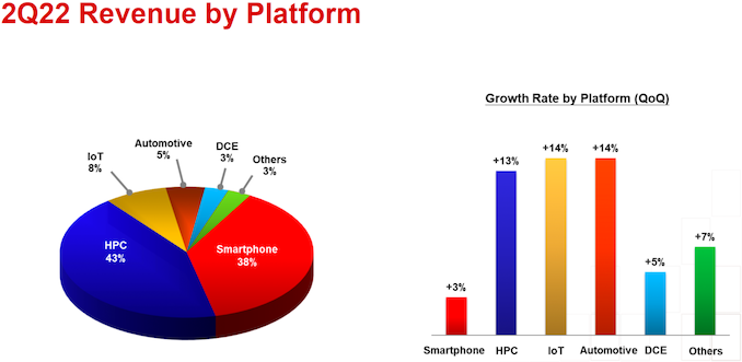
TSMC admits that demand for client-oriented chips is softening, but demand for chips designed to support 5G, AI, and HPC applications still exceeds the company’s abilities to supply.


“While we observe softness in consumer end market segments, other end market segments such as data center and automotive-related remain steady,” said Wei. “We are able to reallocate our capacity to support these areas. Despite the ongoing inventory correction, our customers’ demand continues to exceed our ability to supply. We expect our capacity to remain tight throughout 2022 and our full year growth to be mid-30% in U.S. dollar terms.”


Advanced Nodes to Remain Growth Drivers, Expansions Getting Tougher


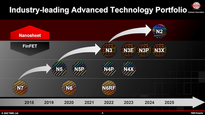
Over half of TSMC’s revenue (51%) comes from chips made using its advanced fabrication technologies (N7 and thinner nodes), which is not particularly surprising as TSMC is one of the only two contract foundries that offer such sophisticated manufacturing processes to clients.


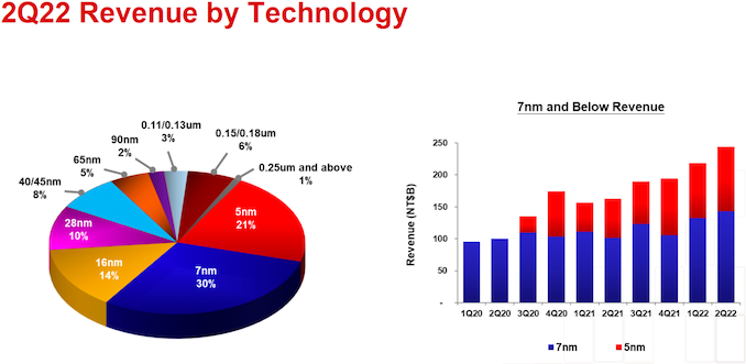
These technologies will be among TSMC’s main growth drivers in the coming years, especially as more customers adopt N7 and more advanced technologies. But more N7/N6 and N5/N4 orders mean that TSMC will need to build more capacity for these nodes, as well as more capacity for N3 and subsequent nodes, which is why the company estimated that its CapEx this year would reach $40 billion – $44 billion.


“With the successful ramp of N5, N4P, N4X, and the upcoming ramp-up of N3, we will expand our customer product portfolio and increase our addressable market,” said the head of TSMC. “The macroeconomic uncertainty may persist into 2023, our technology leadership will continue to advance and support our growth. […] We believe the fundamental structural growth trajectory in the long-term semiconductor demand remains firmly in place. “


The world’s No. 1 contract maker of semiconductors also urges customers to migrate from older nodes to 28nm and specialty technologies as this will ensure capacity availability (as TSMC plans to expand capacity for 28 nm and specialty nodes by 50% by 2025) and denser designs potentially with more features.


Building additional leading-edge, 28 nm, and specialty capacities not only requires massive investments, but TSMC needs to procure additional semiconductor production tools. Whether TSMC is building capacities for its brand-new N3 node or 28nm/specialty technologies, it should be noted that the company needs all kinds of lithography machines for them. An N3-capable fab needs dry litho tools, immersion litho scanners, and EUV-capable equipment. Without required number of dry and immersion scanners, an advanced EUV machine on its own will be useless. Meanwhile, lithography tools are not the only machinery that a fab needs.


Apparently, demand for fab equipment is so high that TSMC will not be able to spend its CapEx budget this year, and some purchases related to advanced (N7 and thinner) and mature nodes will be delayed into 2023. As a result, TSMC’s CapEx this year will be at a lower end of the company’s prediction (around $40 billion) not because it does not want to invest, but because it cannot invest in tools that are not available.


“Our suppliers have been facing greater challenges in their supply chains, which are extending tool delivery lead times for both advanced and mature nodes,” said Wei. “As a result, we expect some of our CapEx this year to be pushed out into 2023.”


ASML Confirms Record Quarterly Bookings


Meanwhile, ASML, the world’s largest producer of lithography tools, this week posted its Q2 2022 revenue of €5.431 billion, a 53% increase year-over-year. During the second quarter, the company supplied (recognized revenue) a total of 91 new lithography systems (up from 59 in Q2 2021), with 12 of those being EUV systems (up from 3 in Q2 2021). 


What is perhaps more important is that ASML’s net bookings for new systems totaled €8.461 billion during the quarter, so the company’s bookings are higher than its quarterly sales. Meanwhile, ASML’s backlog now totals €33 billion and spans multiple years to come, which essentially is a yet another confirmation that it is extremely hard for companies like TSMC to get new tools.


The backlog for DUV machines is now at around 600 units and product order lead time for a new DUV scanner is now about two years. The backlog for EUV tools is well over 100 machines. Meanwhile, ASML says that PO lead time metrics is not exactly relevant since it faces supply chain and own production capacity issues, which means that its partners have to build additional capacity and ASML has to build additional capacity (which takes time) and only then it will be able to supply the tools ordered recently.


For the whole year 2022, ASML expects to ship 55 extreme ultraviolet (EUV) lithography scanners, but recognize revenue of 40 EUV systems valued at €6.40 billion (€160/$140 million per machine) because 15 EUV machines will be so-called fast shipments — a shipment process that skips some of the testing at ASML’s factory and then final testing and formal acceptance are performed at the customer site (which is why revenue acceptance gets deferred). The company also intends to supply 240 deep ultraviolet (DUV) litho tools this year. ASML expects its production capacity to total 60 EUV scanners and 375+ DUV tools in 2023.


Summary


While demand for chips aimed at client/consumer devices is getting softer due to rising inflation and geopolitical uncertainty, the global megatrends like 5G, AI, HPC, and autonomous vehicles are still there and these require loads of advanced system-on-chips, specialty processors, and not-so-advanced things like sensors. Therefore, TSMC is confident of strong demand for chips in the coming years.


But there is a problem with meeting that demand as TSMC is not the only company that is expanding its manufacturing capacity. ASML’s backlog now includes over 100 EUV scanners and around 600 DUV scanners — it will take years for the company to ship these machines. As a result, TSMC has problems with obtaining tools it needs to build additional capacity it needs. It is unclear whether the company has enough capacity to meet all of the potential demand from its largest customers on N3, N4, N5 nodes (Apple, MediaTek, AMD, NVIDIA, etc.), but, ultimately, tool shortages will affect all of its process technologies.


Source: AnandTech – TSMC and ASML: Demand for Chips Remains Strong, But Getting Fab Tools Is Hard

Samsung Portable SSD T7 Shield Review: Flagship PSSD Gets IP65 Avatar

Samsung’s lineup of portable SSDs has enjoyed tremendous success, starting with the T1 back in 2015. The company has been regularly updating their PSSD lineup with the evolution of different high-speed interfaces as well as NAND flash technology. Earlier this year, Samsung launched the Portable SSD T7 Shield, a follow-up to the Portable SSD T7 (Touch) introduced in early 2020. Samsung is mainly advertising the ruggedness / IP65 rating of the T7 Shield as a selling point over the regular Portable SSD T7 and T7 Touch. Today’s review takes a look at the performance and value proposition of the Portable SSD T7 Shield. Our detailed analysis reveals another trick that Samsung has up their sleeve, which makes the T7 Shield a worthy successor to the Portable SSD T7 family.


Source: AnandTech – Samsung Portable SSD T7 Shield Review: Flagship PSSD Gets IP65 Avatar

The Montech Century Gold 650W PSU Review: The New Kid Starts Out Strong

In today’s review, we are taking a look at the Century Gold 650W, an 80Plus Gold certified power supply by Montech. Montech is a Taiwanese company that was founded just six years ago, and yet they already managed to penetrate into the international PC power & cooling market with some surprisingly premium products.


Source: AnandTech – The Montech Century Gold 650W PSU Review: The New Kid Starts Out Strong

Western Digital 22TB WD Gold, Red Pro, and Purple HDDs Hit Retail

Western Digital’s ‘What’s Next’ event back in May 2022 had seen the announcement of its 22TB platform based on ePMR and OptiNAND (with ArmorCache). At the event, WD indicated that the 22TB 10-platter drives would make its market appearance under different product categories – Ultrastar DC HC570 for data centers and enterprises, WD Gold for enterprises, SMEs, and SMBs, WD Red Pro for SMB and SME NAS systems, and WD Purple Pro for surveillance network video recorders.


Today, WD is announcing retail availability of these models along with technical details. All drives have a 3.5″ form-factor and sport a SATA 6 Gbps interface. The drives are equipped with a 512MB cache and have a 7200 rpm spindle speed. The acoustics rating for all of them are the same too – 20 dBA at idle and 32 dBA for the average seek.


Western Digital 2022 22TB Hard Drives – Metrics of Interest
  WD Gold WD Red Pro WD Purple Pro
Rated Workload (TB/yr) 550 300 550
Max. Sustained Transfer Rate (MBps) 291 265 265
Rated Load / Unload Cycles 600K 600K 600K
Unrecoverable Read Errors 1 in 10E15 1 in 10E13 1 in 10E15
MTBF (Hours) 2.5M 1M 2.5M
Power (Idle / Active) (W) 5.7 / 9.3 3.4 / 6.8 5.6 / 6.9
Warranty (Years) 5 5 5
Pricing ?? ?? ??


Based on the above specifications, it is clear that Western Digital has taken the ePMR / OptiNAND / triple-stage actuator platform and tweaked the firmware suitably to cater to different market segments. The Red Pro CMR drive comes with NASware 3.0 firmware that includes features such as adjusting parameters based on the integrated multi-axis shock sensor, maintaining balance using the dual-plane balance control technology, and TLER (Time-Limited Error Recovery) configuration for compatibility with various NAS systems. As is customary for the Red Pro family, the new 22TB drives are recommended for usage in systems with up to 24 bays.


The WD Purple Pro drives meant for network video recordings has firmware tweaked for continuous sequential writes to multiple drive regions simultaneously. WD indicates the capability of the drive to handle up to 64 concurrent HD stream recordings at 3.25 Mbps, and up to 32 streams for machine learning / object detection tasks. Similar to NASware 3.0 in the Red Pro, the custom firmware has a specific moniker – AllFrame AI.


The WD Gold is the flagship in today’s retail launch announcement. It’s firmware is tweaked for the highest possible performance, without focusing on the active and idle power numbers. The ArmorCache feature is specifically turned on in the WD Gold 22TB model only.


The overall push with these high-capacity hard drives is one of TCO. The ability to reduce physical footprint of storage servers for the same capacity can result in significant savings in allied IT costs related to power, cooling, and rack space. Moving forward, WD can hopefully address the plateauing of access speeds compared to capacity (using dual-actuators or some other similar technology). This can make high-capacity HDDs attractive to home consumers / prosumers who may be rightly worried about long RAID rebuild times.


Source: AnandTech – Western Digital 22TB WD Gold, Red Pro, and Purple HDDs Hit Retail

Intel Atlas Canyon (NUC11ATKPE) and GEEKOM MiniAir 11 UCFF PCs Review: Desktop Jasper Lake Impresses

Intel’s low-power Tremont microarchitecture has powered a range of products – from the short-lived Lakefield, to Elkhart Lake in the embedded space, and finally, Jasper Lake in the client computing area. A steady stream of notebooks and motherboards / mini-PCs based on Jasper Lake have become available since the introduction of the series in early 2021. Given their pricing, ultra-compact form-factor (UCFF) machines based on Jasper Lake offer attractive entry-level options in the NUC domain. With a range of SKUs specified for power consumption numbers ranging from 4.8W up to 25W, the product series lends itself to designs that can be either actively or passively cooled. Last week, we had taken a look at two fanless Jasper Lake PCs. Today’s review takes a look at two actively cooled Jasper Lake UCFF systems – the Intel’s flagship Atlas Canyon NUC (NUC11ATKPE), and GEEKOM’s MiniAir 11.


Source: AnandTech – Intel Atlas Canyon (NUC11ATKPE) and GEEKOM MiniAir 11 UCFF PCs Review: Desktop Jasper Lake Impresses

Kingston DataTraveler Max UFD Series Review: New Type-A Thumb Drive Retains NVMe Performance

Kingston’s new products in the portable flash-based external storage space have met with good market reception over the last year or so. Two products in particular – the Kingston XS2000 and the DataTraveler Max – continue to remain unique in the market with no other comparable products being widely available. The Kingston DataTraveler Max USB flash drive (UFD) was introduced in August 2021. It advertised 1GBps-class speeds, low power consumption, and a Type-C interface – all in a thumb drive form-factor. Today, Kingston is expanding the DT Max series with three new drives – all sporting a USB 3.2 Gen 2 Type-A interface. Read on for a detailed look at the performance and characteristics of the new DTMAXA drives.


Source: AnandTech – Kingston DataTraveler Max UFD Series Review: New Type-A Thumb Drive Retains NVMe Performance

Jasper Lake Fanless Showdown: ECS LIVA Z3 and ZOTAC ZBOX CI331 nano UCFF PCs Review

Intel’s Jasper Lake series of products based on the Tremont microarchitecture was launched in early 2021. Since then, we have seen a steady stream of notebooks and motherboards / mini-PCs based on those processors getting introduced in the market.

Ultra-compact form-factor (UCFF) machines based on the Atom series offer attractive entry-level options in the NUC domain. Their low-power nature also lends itself to passively cooled designs. Today, we are looking at two different fanless Jasper Lake UCFF PCs – the ECS LIVA Z3 and the ZOTAC ZBOX CI331 nano.

Our investigation into the performance and behavior of the two PCs revealed some interesting insights into fanless system designs. Read on for a detailed look at what 6W Jasper Lake SKUs can deliver for traditional PC workloads, along with some guidelines on what to look for in passively cooled systems.


Source: AnandTech – Jasper Lake Fanless Showdown: ECS LIVA Z3 and ZOTAC ZBOX CI331 nano UCFF PCs Review

Samsung MUF-256DA USB-C Flash Drive Review: Thumb-Sized Performance Consistency

Portable SSDs have seen great demand over the last few years. Advancements in flash technology and controllers has resulted in compact drives delivering blistering speeds. These advancements have also had their effects on the ubiquitous thumb drives. Samsung’s MUF-256DA is a compact USB Type-C flash drive available in capacities ranging from 64GB to 256GB. Today’s review attempts to figure out how this USB flash drive (UFD) with a native flash controller stacks up against other native controller offerings in the market.


Source: AnandTech – Samsung MUF-256DA USB-C Flash Drive Review: Thumb-Sized Performance Consistency

The AmazonBasics Aurora Vista 1500 UPS Review: Passable Power

AmazonBasics is a private label of products owned by Amazon. The subsidiary was founded back in 2009 and initially offered only basic products, such as cables and office consumables. More and more products are being added under the AmazonBasics label every day. Today, Amazon retails thousands of products under the AmazonBasics label, ranging from paperclips to living room sets. The only common point amongst all of these products is that they are very aggressively priced, usually selling for significantly less than any other competitive product from an established brand.

In this review, we are having a look at a very popular low-cost UPS that Amazon distributes under the AmazonBasics label, the AmazonBasics Aurora Vista 1500VA. Much like its name suggests, it is a very basic design with minimal features, yet it is very aggressively priced. Taking the renowned Amazon customer service into account, it seems like an amazing deal for that kind of output.


Source: AnandTech – The AmazonBasics Aurora Vista 1500 UPS Review: Passable Power

The AMD Ryzen 7 5800X3D Review: 96 MB of L3 3D V-Cache Designed For Gamers

The level of competition in the desktop CPU market has rarely been as intensive as it has been over the last couple of years. When AMD brought its Ryzen processors to market, it forced Intel to reply, and both have consistently battled in multiple areas, including core count, IPC performance, frequency, and ultimate performance. The constant race to improve products, stay ahead of the competition, and meet customers’ changing needs has also sent the two companies off of the beaten paths at times, developing even wilder technologies in search of that competitive edge.

In the case of AMD, one such development effort has culminated with 3D V-Cache packaging technology, which stacks a layer of L3 cache on top of the existing CCD’s L3 cache. Owing to the fact that while additional cache is beneficial to performance, large quantities of SRAM are, well, large, AMD has been working on how to place more L3 cache on a CPU chiplet without blowing out the die size altogether. The end result of that has been the stacked V-Cache technology, which allows the additional cache to be separately fabbed and then carefully placed on top of a chip to be used as part of a processor.

For the consumer market, AMD’s first V-Cache equipped product is the Ryzen 7 5800X3D. Pitched as the fastest gaming processor on the market today, AMD’s unique chip offers eight cores/sixteen threads of processing power, and a whopping 96 MB of L3 cache onboard. Essentially building on top of the already established Ryzen 7 5800X processor, the aim from AMD is that the additional L3 cache on the 5800X3D will take gaming performance to the next level – all for around $100 more than the 5800X.

With AMD’s new gaming chip in hand, we’ve put the Ryzen 7 5800X3D through CPU suite and gaming tests to see if it is as good as AMD claims it is.


Source: AnandTech – The AMD Ryzen 7 5800X3D Review: 96 MB of L3 3D V-Cache Designed For Gamers

Samsung Starts 3nm Production: The Gate-All-Around (GAAFET) Era Begins

Capping off a multi-year development process, Samsung’s foundry group sends word this morning that the company has officially kicked off production on its initial 3nm chip production line. Samsung’s 3nm process is the industry’s first commercial production process node using gate-all-around transistor (GAAFET) technology, marking a major milestone for the field of silicon lithography, and potentially giving Samsung a major boost in its efforts to compete with TSMC.


The relatively spartan announcement from Samsung, which comes on the final day of Q2, announces that Samsung has begun production of chips on a GAAFET-enabled 3nm production line. The company is not disclosing the specific version of the node used here, but based on previous Samsung roadmaps, this is undoubtedly Samsung’s initial 3GAE process – essentially, Samsung’s earliest process node within a family. According to Samsung, the line will initially be used to produce chips for “high performance, low power computing”, with mobile processors to come later. Samsung’s early process nodes are traditionally reserved for the company’s internal use, so while Samsung isn’t announcing any specific 3nm chips today, it’s only a matter of time until we see a 3nm SoC announces from Samsung LSI.


Samsung has, for the most part, been quiet about its progress on 3nm/GAAFET this year. The last significant news we heard from the company on the matter was several months ago at the company’s Foundry Forum event, where the company reiterated plans to get 3GAE into production by the end of 2022. Given the previous silence and the cutting-edge nature of the technology, there had been more than some concern that 3GAE would be delayed past 2022 – adding on to delays that pushed the tech out of its original 2021 launch window – but with today’s announcement Samsung seems to want to put that to rest.


With that said, the devil is in the detail in these announcements, especially as to what’s said versus not said. Taken literally, today’s announcement from Samsung notably does not include any mention of “high volume” manufacturing, which is the traditional milestone for when a process node is ready for commercial use. So by merely saying 3nm is in production, Samsung’s announcement leaves the company with a fair bit of wiggle room with regards to just how many chips they’re capable of producing – and at what yields. The company was producing test chips back in 2021, so the matter is more nuanced than just firing up the fab, so the line between PR and productization is fuzzy, to say the least.


Still, today’s announcement is a major moment for Samsung, who has been working on 3nm/GAAFET technology since before 2019, when they initially announced the technology. Samsung’s specific flavor of GAA transistor technology is Multi Bridge Channel FET (MBCFET), which is a nanosheet-based implementation. Nanosheet-based FETs are extremely customizable, and the width of the nanosheet is a key metric in defining the power and performance characteristics: the higher the width, the higher the performance (at higher power). As a result, transistor designs that focus on low power can use smaller nanosheets, while logic that requires higher performance can go for the wider sheets.


Along with today’s production announcement, Samsung has also offered some updated size and performance figures comparing 3GAE to older nodes. Officially, 3GAE can offer 45% reduced power consumption or 23% improved performance compared to Samsung’s 5nm process (the company doesn’t state which flavor), with an overall reduction in feature size of 16%. These figures are notably different from Samsung’s previous (2019) figures, which compared the tech to Samsung’s 7LPP node. Given the change in baselines, it’s not clear at this point whether 3GAE is living up to Samsung’s initial claims, or if they’ve had to back off a bit for the initial version of their 3nm technology.


What is clear, however, is that Samsung has more significant improvements in mind for the second iteration of 3nm, which we know is 3GAP(lus). According to today’s press release, Samsung is expecting a 50% power reduction or 30% performance improvement versus the same 5nm baseline, with a much greater 35% area reduction. Today’s announcement doesn’t offer a date for 3GAP, but per previous roadmaps, 3GAP is expected to land around a year after 3GAE. 3GAP is also when we expect to see Samsung open the door to outside customers, though given the harsh competitive environment, nothing should be taken for granted.


Samsung Process Roadmap (July 2021)


The launch of Samsung’s 3nm process tech comes as the company is working to regain its footing against arch rival TSMC, who has clearly pulled into the lead in the 5nm/4nm generation. The gap between TSMC and Samsung has been wide enough that major customers such as Qualcomm have been porting high-performance chips like the Snapdragon 8 series from Samsung to TSMC, and at this point Samsung has seen few major 5nm/4nm wins compared to TSMC. If everything goes well, being the first fab with GAAFET tech could give Samsung a temporary-but-material advantage over TSMC, whose 3nm process is still using older FinFET-style transistors. But in order to pull that off, Samsung will need to reverse their earlier technical problems and deliver a performant, high-yielding process that’s far enough ahead to woo skeptical customers.


Source: AnandTech – Samsung Starts 3nm Production: The Gate-All-Around (GAAFET) Era Begins

ASRock Releases Raptor Lake BIOS Updates For Its 600 Series Motherboards

While Intel has yet to officially announce its next (13th) generation of Core processors, this isn’t stopping motherboard manufacturers from releasing products for them. Always eager to slide ahead of the competition and spur on new sales towards the later half of a platform’s lifecycle, mobo makers are already releasing BIOSes that support Intel’s future chips – parts which, officially speaking, don’t even exist (yet).


Leading this charge is ASRock, who today has released a wave of new BIOSes for its 600 series motherboards designed to support Intel’s next generation of processors. Looking to the future, the wave of BIOS updates is the vast majority of its first-generation LGA1700 motherboards, including their Z690, H670, B660, and H610 models.


At present, Intel has not officially announced its Raptor Lake processors yet, which are set to be Intel’s next-generation of processors for desktops. This is an interesting move from ASRock, which means users currently with an ASRock 600-series motherboard can update the firmware now and not have to worry about installing the ‘next-gen’ later on.


ASRock’s EZ Update utility, alongside its models with BIOS Flashback, can install the update with a USB stick with the core file on it. However, it remains to be seen if pre-existing 600-series boards will be updated at the retail/distribution level before the launch of Raptor Lake.


The current Intel Z690 chipset features and specifications


The biggest question, though, is why right now? Intel hasn’t gone as far as announcing its 13th Gen Core series yet, although it is expected to be sometime by the end of this year. Officially, Intel has kept things about the upcoming Raptor Lake processors under wraps, and there is still very little to go on outside of unconfirmed sources and ‘leaks.’


It’s also worth noting that Intel is likely to announce a new motherboard chipset for its 13th Gen Core series processors, likely named Z790 following previous launches, which will also be on the LGA 1700 socket. This is much like with the release of the Z590 chipset, which also featured support for 11th and 10th Generation Core series processors.


Outside of ASRock’s announcement, other motherboard vendors have been tight-lipped about the upcoming 13th Generation Core series processors and Intel. It remains to be seen if other vendors now choose to follow suit with ASRock in releasing firmware for unannounced processors, especially seeing as there are usually teething problems with launch day firmware, let alone firmware released months in advance.


Source: ASRock


Source: AnandTech – ASRock Releases Raptor Lake BIOS Updates For Its 600 Series Motherboards

TSMC: N2 To Start With Just GAAFETs, Add Backside Power Delivery Later

When TSMC initially introduced its N2 (2 nm class) process technology earlier this month, the company outlined how the new node would be built on the back of two new cutting-edge fab techniques: gate-all-around transistors, and backside power rails. But, as we’ve since learned from last week’s EU symposium, TSMC’s plans are a bit more nuanced than first announced. Unlike some of their rivals, TSMC will not be implementing both technologies in the initial version of their N2 node. Instead, the first iteration of N2 will only be implementing gate-all-around transistors, with backside power delivery to come with a later version of the node.


So far, TSMC has mentioned two distinctive features of N2: nano sheet gate-all-around (GAA) transistors, and backside power rails. GAA transistors have two unique advantages over FinFETs: they solve many challenges associated with the leakage current since GAAFET’s channels are horizontal and are surrounded by gates around all four sides. Meanwhile, backside power rail enabled improved power delivery to transistors, which increases performance and lowers power consumption.


But, as it turns out, TSMC is not planning to start with both nanosheet GAA transistors and backside power rails in the initial generation of its N2 process technology. As disclosed by the company last week at their EU symposium, the first generation of N2 will only feature gate-all-around transistors. Backside power delivery, on the other hand, will come later with more advanced implementations of N2.


At this point the company hasn’t said too much as to why they’re not rolling out backside power delivery as part of their initial N2 node. But, in discussing the bifurcation, TSMC has noted that backside power delivery will ultimately add additional process steps, which the company is seemingly looking to avoid on their first try with GAAFETs.


The lack of backside power delivery in the original version of the N2 fabrication technology perhaps explains rather moderate performance improvement of N2 when compared to N3E node. While for high-performance computing (CPUs, accelerators, etc.) a 10% to 15% performance improvement at the same power and complexity does not seem to be impressive, a 25% to 30% power drop at the same speed and complexity seems to be very good for mobile applications. 


Advertised PPA Improvements of New Process Technologies

Data announced during conference calls, events, press briefings and press releases
  TSMC
N5

vs

N7
N3

vs

N5
N3E

vs

N5
N2

vs

N3E
Power -30% -25-30% -34% -25-30%
Performance +15% +10-15% +18% +10-15%
Chip Density* ? ? ~1.3X >1.1X
Volume

Manufacturing
Q2 2022 H2 2022 Q2/Q3 2023 H2 2025


*Chip density published by TSMC reflects ‘mixed’ chip density consisting of 50% logic, 30% SRAM, and 20% analog. 


Considering that TSMC always offers multiple versions of its nodes, that TSMC has several variants planned for N2 is not all that surprising. Nonetheless, it is a bit odd to see that TSMC is taking a rather long road to backside power delivery.


Compared and contrasted to the competition, this will end up being a notable difference from how rival Intel is planning to handle their own GAAFET/backside power transition with the Intel 20A process. Intel intends to introduce its GAA RibbonFET transistors and PowerVia interconnects together in mid-2024 – going so far as to create an internal pseudo node just to focus on RibbonFET development. TSMC, on the other hand, is taking a more cautious approach to risks and innovations, one which potentially has TSMC moving at a slower pace, but is also an approach that has traditionally been a better fit for TSMC’s need to deliver more constant and consistent updates to its fab offerings.


And while we’re still a few years out, it will be interesting to see what this means for the competitiveness of TSMC’s first-generation N2 node. Will a GAAFET process without backside power delivery be at a meaningful disadvantage? Per current schedules, we’ll find out the answer to that in the second half of 2025, when TSMC’s first N2 node is slated to enter high-volume manufacturing (HVM).


Source: AnandTech – TSMC: N2 To Start With Just GAAFETs, Add Backside Power Delivery Later

TSMC to Customers: It's Time to Stop Using Older Nodes and Move to 28nm

We tend to discuss leading-edge nodes and the most advanced chips made using them, but there are thousands of chip designs developed years ago that are made using what are now mature process technologies that are still widely employed by the industry. On the execution side of matters, those chips still do their jobs as perfectly as the day the first chip was fabbed which is why product manufacturers keep building more and more using them. But on the manufacturing side of matters there’s a hard bottleneck to further growth: all of the capacity for old nodes that will ever be built has been built – and they won’t be building any more. As a result, TSMC has recently begun strongly encouraging its customers on its oldest (and least dense) nodes to migrate some of their mature designs to its 28 nm-class process technologies.


Nowadays TSMC earns around 25% of its revenue by making hundreds of millions of chips using 40 nm and larger nodes. For other foundries, the share of revenue earned on mature process technologies is higher: UMC gets 80% of its revenue on 40 nm higher nodes, whereas 81.4% of SMIC’s revenue come from outdated processes. Mature nodes are cheap, have high yields, and offer sufficient performance for simplistic devices like power management ICs (PMICs). But the cheap wafer prices for these nodes comes from the fact that they were once, long ago, leading-edge nodes themselves, and that their construction costs were paid off by the high prices that a cutting-edge process can fetch. Which is to say that there isn’t the profitability (or even the equipment) to build new capacity for such old nodes.


This is why TSMC’s plan to expand production capacity for mature and specialized nodes by 50% is focused on 28nm-capable fabs. As the final (viable) generation of TSMC’s classic, pre-FinFET manufacturing processes, 28nm is being positioned as the new sweet spot for producing simple, low-cost chips. And, in an effort to consolidate production of these chips around fewer and more widely available/expandable production lines, TSMC would like to get customers using old nodes on to the 28nm generation.


“We are not currently [expanding capacity for] the 40 nm node” said Kevin Zhang, senior vice president of business development at TSMC. “You build a fab, fab will not come online [until] two year or three years from now. So, you really need to think about where the future product is going, not where the product is today.”


While TSMC’s 28nm nodes are still subject to the same general cost trends as chip fabs on the whole – in that they’re more complex and expensive on a per-wafer basis than even older nodes – TSMC is looking to convert customers over to 28nm by balancing that out against the much greater number of chips per wafer the smaller node affords. Therefore, while companies will have to pay more, they also stand to to get more in terms of total chips. And none of this takes into account potential ancillary benefits of a newer node, such as reduced power consumption and potentially greater clockspeed (performance) headroom.


“So, lots of customers’ product today is at, let’s say 40 nm or even older, 65 nm,” said Zhang.  They are moving to lower advance nodes. 20/28 nm is going to be a very important node to support future specialty. […] We are working with customer to accelerate [their transition]. […] I think the customer going to get a benefit, economic benefit, scaling benefit, you have a better power consumption.  but they’ve already got a chip that works. Why? Oh, then you could say why we do advanced technology. Yeah. Yeah. I mean, it’s, uh, find just the nature of the summit is you go to a next node, you get a better performance and better power and overall you get a system level benefit.”


In addition to multiple 28nm nodes designed for various client applications, TSMC is expanding its lineup of specialty 28nm and 22nm (22ULP, 22ULL) process technologies to address a variety of chip types that currently rely on various outdated technologies. As with the overall shift to 28nm, TSMC is looking to corral customers into using the newer, higher density process nodes. And, if not 28nm/22nm, then customers also have the option of transitioning into even more capable FinFET-based nodes, which are part of TSMC’s N16/N12 family (e.g., N12e for IoT). 


Source: AnandTech – TSMC to Customers: It’s Time to Stop Using Older Nodes and Move to 28nm

As HPC Chip Sizes Grow, So Does the Need For 1kW+ Chip Cooling

One trend in the high performance computing (HPC) space that is becoming increasingly clear is that power consumption per chip and per rack unit is not going to stop with the limits of air cooling. As supercomputers and other high performance systems have already hit – and in some cases exceeded these limits – power requirements and power densities have continued to scale up. And based on the news from TSMC’s recent annual technology symposium, we should expect to see this trend continue as TSMC lays the groundwork for even denser chip configurations.


The problem at hand is not a new one: transistor power consumption isn’t scaling down nearly as quickly as transistor sizes. And as chipmakers are not about to leave performance on the table (and fail to deliver semi-annual increases for their customers), in the HPC space power per transistor is quickly growing. As an additional wrinkle, chiplets are paving the way towards constructing chips with even more silicon than traditional reticle limits, which is good for performance and latency, but even more problematic for cooling.


Enabling this kind of silicon and power growth has been modern technologies like TSMC’a CoWoS and InFO, which allow chipmakers to build integrated multi-chiplet system-in-packages (SiPs) with as much a double the amount of silicon otherwise allowed by TSMC’s reticle limits. By 2024, advancements of TSMC’s CoWoS packaging technology will enable building even larger multi-chiplet SiP, with TSMC anticipating stitching together upwards of four reticle-sized chiplets, This will enable tremendous levels of complexity (over 300 billion transistor per SiP is a possibility that TSMC and its partners are looking at) and performance, but naturally at the cost of formidable power consumption and heat generation. 


Already, flagship products like NVIDIA’s H100 accelerator module require upwards of 700W of power for peak performance. So the prospect of multiple, GH100-sized chiplets on a single product is raising eyebrows – and power budgets. TSMC envisions that several years down the road there will be multi-chiplet SiPs with a power consumption of around 1000W or even higher, Creating a cooling challenge.


At 700W, H100 already requires liquid cooling; and the story is much the same for the chiplet based Ponte Vecchio from Intel, and AMD’s Instinct MI250X. But even traditional liquid cooling has its limits. By the time chips reach a cumulative 1 kW, TSMC envisions that datacenters will need to use immersion liquid cooling systems for such extreme AI and HPC processors. Immersion liquid cooling, in turn, will require rearchitecting datacenters themselves, which will be a major change in design and a major challenge in continuity.


The short-tem challenges aside, once datacenters are setup for immersion liquid cooling, they will be ready for even hotter chips. Liquid immersion cooling has a lot of potential for handling large cooling loads, which is one reason why Intel is investing heavily in this technology in an attempt to make it more mainstream.


In addition to immersion liquid cooling, there is another technology that can be used to cool down ultra-hot chips — on-chip water cooling. Last year TSMC revealed that it had experimented with on-chip water cooling and said that even 2.6 kW SiPs could be cooled down using this technology. But of course, on-chip water cooling is an extremely expensive technology by itself, which will drive costs of those extreme AI and HPC solutions to unprecedented levels.


None the less, while the future isn’t set in stone, seemingly it has been cast in silicon. TSMC’s chipmaking clients have customers willing to pay a top dollar for those ultra-high-performance solutions (think operators of hyperscale cloud datacenters), even with the high costs and technical complexity that entails. Which to bring things back to where we started, is why TSMC has been developing CoWoS and InFO packaging processes on the first place – because there are customers ready and eager to break the reticle limit via chiplet technology. We’re already seeing some of this today with products like Cerebras’ massive Wafer Scale Engine processor, and via large chiplets, TSMC is preparing to make smaller (but still reticle-breaking) designs more accessible to their wider customer base.


Such extreme requirements for performance, packaging, and cooling not only push producers of semiconductors, servers, and cooling systems to their limits, but also require modifications of cloud datacenters. If indeed massive SiPs for AI and HPC workloads become widespread, cloud datacenters will be completely different in the coming years.


Source: AnandTech – As HPC Chip Sizes Grow, So Does the Need For 1kW+ Chip Cooling

The Gigabyte UD1000GM PG5 1000W PSU Review: Prelude to ATX 3.0

In today’s review, we are taking a look at the first-ever PSU released with the new 12VHPWR connector, the GIGABYTE UD1000GM PG5. Although the unit is not ATX v3.0 compliant, GIGABYTE upgraded one of their currently available platforms to provide for a single 600W video card connector in an effort to entice early adopters.


Source: AnandTech – The Gigabyte UD1000GM PG5 1000W PSU Review: Prelude to ATX 3.0

AMD Updates Ryzen Embedded Series, R2000 Series With up to Four Cores and Eight Threads

One area of AMD’s portfolio that perhaps doesn’t garner the same levels of attention as its desktop, mobile, and server products is its embedded business. In early 2020, AMD unveiled its Ryzen Embedded R1000 platform for the commercial and industrial sectors and the ever-growing IoT market, with low-powered processors designed for low-profile systems to satisfy the mid-range of the market.


At Embedded World 2022 in Nuremberg, Germany, AMD has announced its next-generation of Ryzen Embedded SoCs, the R2000 series. Offering four different SKUs ranging from 2C/4T up to 4C/8T, which is double the core count of the previous generation, AMD claims that the R2000 series features up to 81% higher CPU and graphics performance.


The AMD Ryzen Embedded R2000 Series compared to the previous generation (R1000), now has double the core count, with a generational swing from Zen to the more efficient and higher performance Zen+ cores. All four SKUs announced feature a configurable TDP, with the top SKU, the R2544, operating at between 35 and 54 W. More in line with the lower power target of these SoCs, the bottom SKU (R2312) has a configurable TDP of between 12 and 35 W.


AMD Ryzen Embedded R2000-Series APUs
AnandTech Core/

Thread
Base

Freq (MHz)
1T Boost

Freq (MHz)
Memory

Support
L2

Cache
L3

Cache
GPU

CU’s
TDP

Range

(W)
Launch

 (Expected)  
R2544 4 8 3350 3700 DDR4-3200 2 MB 4 MB 8 35-54 October 22
R2514 4 8 2100 3700 DDR4-2667 2 MB 4 MB 8 12-35 October 22
R2314 4 4 2100 3500 DDR4-2667 2 MB 4 MB 6 12-35 In Production
R2312 2 4 2700 3500 DDR4-2400 1 MB 2 MB 3 12-25 In Production


Another element delivering additional performance compared to the previous generation is better iGPU performance via increasing the number of Radeon Vega graphics compute units. The entry R2312 SKU comes with 3 CUs, while the R2544 comes with 8 CUs. The Ryzen Embedded R2000 series also benefits from newer video decode and display processor blocks, bringing support for decoding 4Kp60 video and driving up to three 4K displays.


AMD has also equipped the SoCs with 16 PCIe Gen 3 lanes on the R2314, R2514, and R2544 SKUs, while the R2312 gets eight. The R2000 series has support for two SATA 3.0 ports, up to six USB ports with a mixture of USB 3.2 G2 and USB 2.0, and OS support for Microsoft Windows 11/10 and Linux Ubuntu LTS. 


The application benefits of AMD’s Ryzen Embedded R2000 series include the commercial and industrial sectors, as well as robotics, with a planned product availability of up to 10 years, ensuring a long life cycle for each product. Some of AMD’s Ryzen Embedded R2000’s Ecosystem partners include Advantech for its gaming and gambling machines, as well as DFI, IBASE, and Sapphire, so these new SoCs are already being adopted and planned into existing thin-client and small form factor systems.


AMD states that the Ryzen Embedded R2544 (4C/8T) and R2514 (4C/8T) will be available sometime in October 22, while the R2314 and R2312 SKUs are currently in production.


Source: AMD


Source: AnandTech – AMD Updates Ryzen Embedded Series, R2000 Series With up to Four Cores and Eight Threads