AMD EXPO Memory Technology: One Click Overclocking Profiles For Ryzen 7000

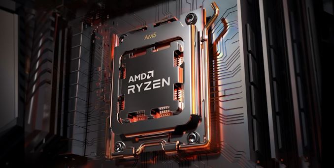
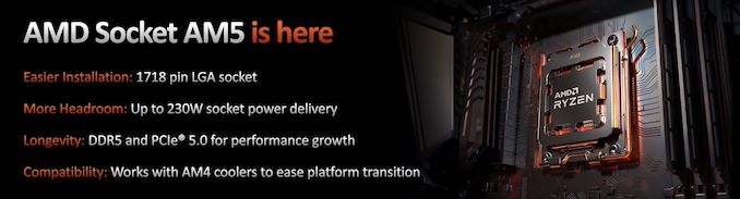
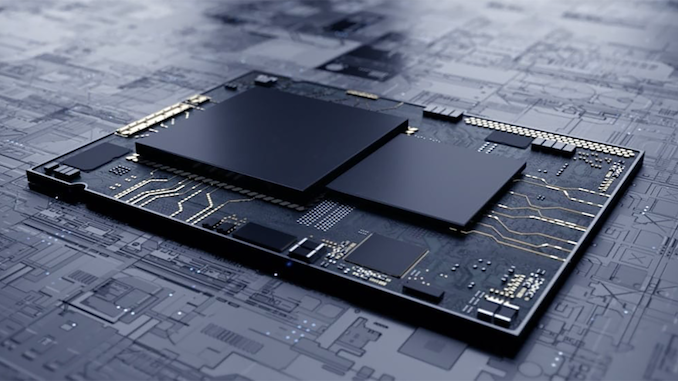
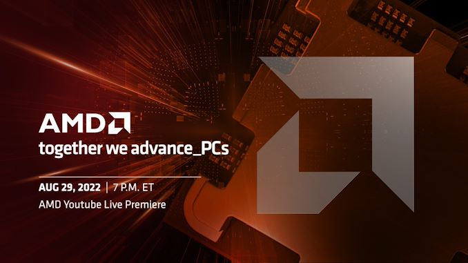
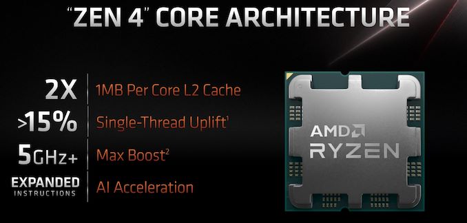
During AMD’s ‘together we advance_PCs event, the company unveiled its latest Zen 4-based Ryzen 7000 processors to the world, as well as its AM5 platforms, including X670E, X670, B650E, and B650. AMD also announced what it calls AMD EXPO, a new technology for overclocking DDR5 memory. In conjunction with this announcement, AMD has partnered with memory manufacturers including ADATA, Corsair, G.Skill, GeIL, and Kingston Technology to bring AMD Ryzen 7000 optimized kits of DDR5 memory to the market, with 15 (or more) of these set to be available on launch day on September 27th.


AMD EXPO stands for EXtended Profiles for Overclocking and is designed to provide users with high-end memory overclocking when used in conjunction with AMD’s Ryzen 7000 series processors. Similar to Intel’s preexisting X.M.P (Extreme Memory Profile) technology found on most consumer-level memory kits designed for desktop Intel platforms, AMD’s EXPO technology aims to do the same, but as an open standard with an emphasis on providing the best settings for AMD platforms.


AMD EXPO Technology: Like X.M.P, but Optimized for Ryzen 7000


The premise of AMD EXPO is that it will be a one-click DDR5 overclocking function for AM5 motherboards, and AMD claims that EXPO overclocked memory kits will offer up to 11% higher gaming performance at 1080p, although it hasn’t quantified how it came to this figure. AMD did, however, state that it is expecting (at least) 15 kits of DDR5 memory with AMD EXPO at launch on September 27th, with rates of up to DDR5-6400.


AMD EXPO, on the surface, is essentially an X.M.P profile specifically designed for AMD’s Ryzen 7000 (Zen 4) processors. Although AMD hasn’t gone into finer details on how it differs from X.M.P, beyond the fact that it will be royalty and licensing fee free.


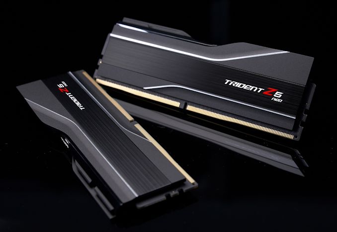
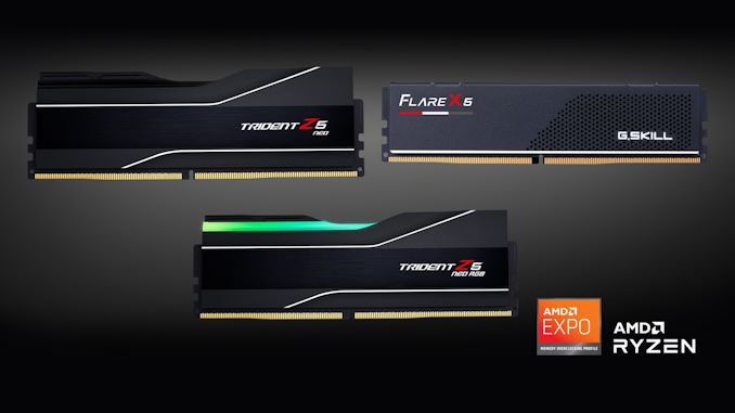
G.Skill Trident Z5 Neo DDR5 memory with AMD EXPO certification


It is worth noting that DDR5 memory with X.M.P profiles will be supported on Ryzen 7000 platforms. Still, AMD EXPO adds an additional layer of ‘compatibility’ with AMD systems, as EXPO DIMMs will be optimized for use on AMD platforms (as opposed to X.M.P. kits chiefly being optimized for Intel platforms).


AMD EXPO does have one caveat associated with it; AMD EXPO is classed as overclocking in AMD’s own eyes, and according to its footnotes, it does void the warranty.


The footnote on the AMD EXPO landing page states as follows:


Overclocking and/or undervolting AMD processors and memory, including without limitation, altering clock frequencies / multipliers or memory timing / voltage, to operate outside of AMD’s published specifications will void any applicable AMD product warranty, even when enabled via AMD hardware and/or software. This may also void warranties offered by the system manufacturer or retailer. Users assume all risks and liabilities that may arise out of overclocking and/or undervolting AMD processors, including, without limitation, failure of or damage to hardware, reduced system performance and/or data loss, corruption or vulnerability. GD-106


Similar to how Intel operates with X.M.P profiles being applied, using AMD EXPO will technically void the warranty, which seems odd given this is AMD’s technology designed to offer adopters of Ryzen 7000 and AM5 an additional boost to performance through certification. When overclocking, doing so is always at the user’s risk. Still, with a certification such as AMD EXPO offers, it seems a little odd that AMD is recommending optimized memory for its platform but also voids the processor’s warranty.


AMD EXPO: 15 Different DDR5 Kits Available At Launch


As we previously mentioned, AMD says that there should be 15 kits of DDR5 with support for AMD EXPO ready to launch when Ryzen 7000 is released on September 27th. Some of these kits include ADATA Caster RGB and Lancer RGB models, with GeiL EVO V models and Kingston Technology Fury Beast and RGB enabled models.


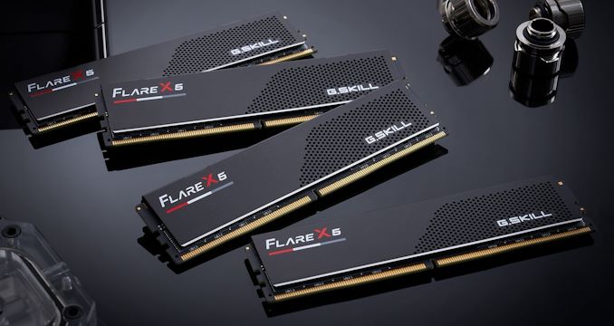
G.Skill Flare X5 Memory in black with AMD EXPO certification


Corsair and G.Skill sent us information on what it is launching alongside Ryzen 7000 on September 27th. Starting with G.Skill, it announced three new kits of DDR5 for Ryzen 7000, including its Trident Z5 Neo RGB, regular Trident Z5 Neo, and the Flare X5 series. The flagship for its AMD EXPO memory is the Trident Z Neo, with four different varieties of DDR5-6000 set for launch, each with different latencies and capacities, as outlined in the table below.


G.Skill AMD EXPO DDR5 Memory (as of 08/30)
Memory Frequency CL Timing Capacity
Trident Z5 Neo + RGB Neo DDR5-6000 30-38-38-96 2 x 16 GB
30-40-40-96 2 x 32 GB
32-38-38-96 2 x 16 / 2 x 32 GB
36-36-36-96 2 x 16 GB
Flare X5 DDR5-5600 28-34-34-89 2 x 16 / 2 x 32 GB
30-36-36-89
36-36-36-89


The Trident Z5 Neo and RGB Neo share the same specifications, but the RGB version includes a customizable LED lightbar. The top SKU from G.Skill with AMD EXPO at launch will be the DDR5-6000 CL30-38-38-96 kit, which is available in capacities of 2 x 16 GB (32 GB). The Flare X5 replaces the older Flare X series for DDR4 and features a lower profile heatsink at just 33 mm tall; this makes it more compatible for users with space restrictions of large tower coolers that restrict larger and more aggressive heatsink designs such as the Trident Z5 Neo.


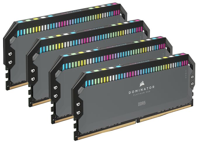
New Corsair Dominator Platinum RGB DDR5 for AMD Ryzen 7000


Focusing on what Corsair has announced for its AMD EXPO certified memory, it has two new varieties of DDR5 memory. This includes new premium Dominator Platinum RGB DDR5, Vengeance DDR5, and non-RGB enabled Vengeance DDR5, all designed specifically for AMD and Ryzen 7000. The top SKU from Corsair is the Dominator Platinum RGB 32 GB (2 x 16 GB) kit with speeds of DDR5-6000 and latencies of CL30-36-36-76. The Dominator Platinum RGB DDR5 memory for AMD EXPO will also be available in 64 GB (2 x 32 GB) kits, with speeds of DDR5-5600 CL36 and DDR5-5200 CL40 varieties. 


The Corsair Vengeance RGB with AMD EXPO profiles will reach up to DDR5-6000 CL30 but will also be available in DDR5-5600 CL36 and DDR5-5200 CL40. At the time of writing, the non-RGB enabled Vengeance for AM5 will max out at DDR5-5600 CL36, with options also available in DDR5-5200 CL40 in both 2 x 16 GB (32 GB) and 2 x 32 GB (64 GB) kits.


The AMD EXPO DDR5 memory kits will launch at the same time as AMD’s Ryzen 7000 desktop processors and AMD X670E and X670 motherboards: September 27th. None of the memory vendors have provided us with any pricing at the time of writing.


Source: AMD, Corsair, & G.Skill


Source: AnandTech – AMD EXPO Memory Technology: One Click Overclocking Profiles For Ryzen 7000

AMD Announces B650E Chipset for Ryzen 7000: PCIe 5.0 For Mainstream

Over the last couple of months, the rumor mill surrounding AMD’s impending Ryzen 7000 processors for desktops has been in overdrive. Although Lisa Su unveiled Zen 4 back at CES 2022, it’s been anticipated that the new AM5 platform would include multiple chipsets, much like AM4 has over 500+ motherboard lifespan from X370, X470, X570, and every chipset in between.


AMD announced its X670E, X670, and B650 chipsets during the AMD Keynote at Computex 2022, and this evening, AMD has announced a fourth chipset for Ryzen 7000, the B650E chipset. The B650E chipset will run alongside the already announced B650 chipset, but as it’s part of AMD’s ‘Extreme’ series of chipsets, it will benefit from PCIe 5.0 lanes to at least one M.2 slot, as well as optional support for PCIe 5.0 to a PCIe graphics slot, features not available with standard B650 boards.


During AMD’s Keynote at Computex 2022, AMD’s CEO Lisa Su unveiled three AM5 chipsets designed to harness the power of its 5 nm Zen 4 cores within the Ryzen 7000 processors. We already knew the AM5 socket was based around a Lane Grid Array (LGA) socket with 1718 pins, aptly named LGA1718. Some of the significant benefits coming to AM5 include native PCIe 5.0 support from the CPU, not just for use with the PCIe slots, but also in the way of PCIe 5.0 storage, where the first consumer drives are expected to start rolling out in November 2022.


AMD’s latest announcement of the B650E (Extreme) chipset gives motherboard vendors and users the option of a lower-cost platform but without sacrificing the longevity and expansion support of PCIe 5.0. The X670E chipset is reserved for its most premium models, such as the flagship ASUS ROG Crosshair X670E Extreme motherboard, unveiled at Computex 2022.


AMD AM5 Chipset Comparison
Feature X670E X670 B650E B650
CPU PCIe (PCIe) 5.0 (Mandatory)

2 x16 Slots
4.0

(5.0 Optional)
4.0

(5.0 Optional)
4.0

(5.0 Optional)
CPU PCIe (M.2 Slots) At Least 1 PCIe 5.0 Slot PCIe 4.0

(5.0 Optional)
Total CPU PCIe Lanes 24
SuperSpeed USB 20Gbps

(USB 3.2 Gen 2×2)
Up To 14
DDR5 Support Quad Channel (128-bit bus)

Speeds TBD
Wi-Fi 6E Yes
Overclocking Support Y Y Y Y
Available September 2022 October 2022


Using PCIe 5.0 lanes requires a more premium PCB, usually with more layers which allows the tracks to keep signal integrity, but this typically adds cost. The existence of the B650E chipset will enable vendors to use more expensive PCIe 5.0 laning with more modest controller sets, which allow vendors to offset the cost. Ideally, it gives users a broader and more future-proof platform to upgrade with, but without breaking the bank on unnecessary controller sets; users wanting the best controller sets should opt for X670 or X670E.


This ultimately means that AMD will have a mainstream platform that has PCIe 5.0 by default (B650E) and a lower-cost alternative with just PCIe 4.0 lanes to the PEG and M.2 slots. AMD is strongly prodding motherboard vendors to offer at least one PCIe 5.0 M.2 slot for storage on most of their boards, as this is one of the main benefits of AMD’s AM5 platform.


As announced by AMD during its together we advance_PCs event, the Ryzen 7000 processors for desktop will launch on September 27th, with both motherboards from the X670E and X670 chipsets. The motherboards featuring the B650E and B650 chipsets will be available to purchase at a later date in October.


Source: AnandTech – AMD Announces B650E Chipset for Ryzen 7000: PCIe 5.0 For Mainstream

AMD Details Ryzen 7000 Launch: Ryzen 7950X and More, Coming Sept. 27th

AMD’s “together we advance_PCs”l ivestream presentation just wrapped up moments ago, where AMD CEO Dr. Lisa Su set the stage for the release of the next generation of AMD Ryzen desktop CPUs. Building off of AMD’s Ryzen 7000 announcement back at Computex 2022, the eagerly anticipated presentation laid out AMD’s launch plans for their first family of Zen 4 architecture-based CPUs, which will see AMD kick things off with a quartet of enthusiast-focused chips. Topping out with the 16 core Ryzen 9 7950X, AMD’s Ryzen 7000 chips will be launching in just over 4 weeks’ time, on September 27th, with AMD expecting to handily retake the performance crown across virtually all categories of the PC CPU space, from gaming to content creation.

Driving AMD’s gains in this newest generation of desktop CPUs is a combination of architectural improvements underpinning the Zen 4 architecture, as well as moving production of the CPU core chiplets to TSMC’s leading-edge 5nm process. The combination of which will allow AMD to deliver what they are saying is now a 13% increase in IPC over their Zen 3 architecture – up from an 11% claim as of Computex – as well as a sizable increase in CPU clockspeeds. The top-end Ryzen 9 7950X will have a maximum turbo clockspeed of 5.7GHz, 800MHz (16%) higher than the equivalent Ryzen 9 5950X. As a result, AMD expects to deliver a 29% generational increase in single-threaded performance, and even more in multi-threaded workloads.


Source: AnandTech – AMD Details Ryzen 7000 Launch: Ryzen 7950X and More, Coming Sept. 27th

AMD Ryzen 7000 "together we advance_PCs” Live Blog (7pm ET/23:00 UTC)

At long last the date is here. AMD this evening will be broadcasting their “together we advance_PCs” event, which will be focused around the upcoming launch of their next-generation Ryzen 7000 processors.

AMD first unveiled their Ryzen 7000 platform and branding back at Computex 2022, offering quite a few high-level details on the forthcoming consumer processor platform while stating it would be launching in the fall. The new CPU family will feature up to 16 Zen 4 cores using TSMC’s optimized 5 nm manufacturing process for the Core Complex Die (CCD), and TSMC’s 6nm process for the I/O Die (IOD). AMD has not disclosed a great deal about the Zen 4 architecture itself, though their Computex presentation has indicated we should expect a several percent increase in IPC, along with a further several percent increase in peak clockspeeds, allowing for a 15%+ increase in single-threaded performance.

The Ryzen 7000 series is also notable for being the first of AMD’s chiplet-based CPUs to integrate a GPU – in this case embedding it in the IOD. The modest GPU allows for AMD’s CPUs to supply their own graphics, eliminating the need for a discrete GPU just to boot a system while, we expect, providing enough performance for basic desktop work.

Tonight’s presentation, in turn, should finally see AMD moving on to talking about launch details for the Ryzen 7000 CPUs and the associated AM5 platform. That should include performance expectations and a bit more on the motherboards. And, of course, information on the specific chip SKUs that will be hitting the market, including core configurations, clockspeeds, and prices. With any luck we may get a bit more on the Zen 4 architecture as well, as alongside CEO Dr. Lisa Su, CTO Mark Papermaster is slated to present part of the event.

The event is set to kick off tonight, August 29th, at 7pm ET (23:00 UTC). So be sure to join us for our live blog coverage around the announcement of the next generation of AMD desktop CPUs.


Source: AnandTech – AMD Ryzen 7000 “together we advance_PCs” Live Blog (7pm ET/23:00 UTC)

The Cooler Master XG850 Plus Platinum PSU Review: Quality Plus RGB

Today we are having a look at the new XG Plus Platinum series, the latest power supply family from prolific PC peripherals producer Cooler Master. Designed to offer a quality PSU with an extra dash of flair, the RGB fan (and RGB display) equipped XG Plus Platinum is a PSU that’s not quite like anything else on the market. The XG family ranges from 650 to 850 Watts, and today we’re evaluating the most powerful unit in the series, the 850W XG850 Plus Platinum.


Source: AnandTech – The Cooler Master XG850 Plus Platinum PSU Review: Quality Plus RGB

Intel Kicks Off Fab Co-Investment Program with Brookfield: New Fabs to be Jointly Owned

Intel this week introduced its new Semiconductor Co-Investment Program (SCIP) under which it will build new manufacturing facilities in collaboration with investment partners – a sharp departure from the company’s traditional stance of wholly owning its logic fabs. As part of its SCIP initiative, Intel has already signed a deal with Brookfield Asset Management, which will provide Intel about $15 billion to build its fab new fab in Arizona in exchange for a 49% stake in the project. Furthermore, similar co-investment models are set to be used for other fabs in the future.


New Fabs Are Getting Costlier


When Intel announced plans to produce chips for other companies last year (and to a large degree become a contract maker of semiconductors), it marked a significant shift in the company’s business strategy that required Intel to build new manufacturing capacity not only for itself, but for its future clients as well. But modern fabs are exceptionally expensive, as new manufacturing tools — such as contemporary extreme ultraviolet (EUV) lithography scanners — are prohibitively expensive, which makes it considerably harder for the company to execute on its IDM 2.0 strategy from capital point of view. 


To get sufficient capacity for its own products and for its fabless clients in the mid-term future, Intel had to engage into several capital-intensive projects: the $7.1 billion fab expansion in Ireland (which has probably been completed); two new fabs — Fab 52 and Fab 62 — at its Ocotillo site near Chandler, Arizona that were expected to cost $20 billion; an all-new semiconductor production campus in Ohio that will need $20 billion initially and will be a size of a small town as well as will cost up to $100 when fully built; and an all-new production facility near Magdeburg, Germany (which will require an investment of €17 billion).


Intel is set to get billions in incentives from local authorities as well as subsidies from federal governments of the U.S. and Germany to build these fabs. But modern EUV-capable semiconductor production facilities cost about $10 billion (large gigafabs with a capacity of 100,000 wafer starts per month cost north from $20 billion), so financing these projects is particularly challenging even for Intel. Therefore, in a bid to build its new facilities in Arizona the company decided to engage into its co-investment program with Brookfield. 


Intel to Maintain Majority Ownership


Under the terms of the deal, the two companies will co-invest $30 billion in the ongoing expansion of the site with Intel financing 51% and Brookfield backing 49% of the total project cost. Previously Intel planned to invest $20 billion in its Fab 52 and Fab 62, but together with Brookfield the sum has increased to $30 billion. In addition to getting access to additional funding, Intel could also take advantage of Brookfield’s experience in developing infrastructure assets.


By working together with Brookfield, Intel will get $15 billion in free cash flow and will be able to invest more into its new fabs without raising new debt. Also, this will allow Intel to invest more in other projects while “continuing to fund a healthy and growing dividend.” Meanwhile, the $15 billion benefit is “expected to be accretive to Intel’s earnings per share during the construction and ramp phase.”


Perhaps the key part of the announcement is the fact that Intel plans to sign similar deals with co-investors in the future, so expect its upcoming manufacturing capacity to be co-funded by others. Intel will retain majority ownership and operating control of its chip factories, but it will not own 100% of them. Previously the company rarely engaged into joint ventures, the most notable exceptions being IMFT, the company’s NAND flash joint-venture with Micron, and participating in ASML’s customer co-investment program from early 2010s. 


“This landmark arrangement is an important step forward for Intel’s Smart Capital approach and builds on the momentum from the recent passage of the CHIPS Act in the U.S.,” said David Zinsner, Intel CFO. “Semiconductor manufacturing is among the most capital-intensive industries in the world, and Intel’s bold IDM 2.0 strategy demands a unique funding approach. Our agreement with Brookfield is a first for our industry, and we expect it will allow us to increase flexibility while maintaining capacity on our balance sheet to create a more distributed and resilient supply chain.”


Co-ownership of semiconductor manufacturing facilities is not something unheard of the industry. China’s Semiconductor Manufacturing International Co. (SMIC) invests in new fabs together with local authorities of Chinese provinces as well as various asset management companies and/or investment banks (many of which are controlled by China’s federal government). GlobalFoundries used to be co-owned by AMD and Mubadala before the latter acquired AMD’s stake as the chip developer badly needed money. Yet, a co-investment program is something particularly new for Intel, which has always owned 100% of its manufacturing facilities. Ultimately, as it looks like as the semiconductor production is getting more expensive, there is a first time for anything.


Source: AnandTech – Intel Kicks Off Fab Co-Investment Program with Brookfield: New Fabs to be Jointly Owned

ASUS Unveils Crosshair X670E Gene, Premium Micro-ATX AM5 Motherboard for Ryzen 7000

Over the years, multiple motherboards have captivated the market at various price points. Models like the Hero and the Formula are staples of ASUS’s premium but popular ROG-themed offerings. One such series that was once the staple of ASUS’s Intel models based on the micro-ATX form factor was the Gene, last seen in the days of Intel’s 8th and 9th Gen Core series (2019). In what looks to be a resurrection of the Gene series for the release of AMD’s Ryzen 7000 processors based on its latest 5nm Zen 4 microarchitecture, ASUS has announced that the Gene is back via the ROG Crosshair X670E Gene. 


Throughout the years, the ROG Gene series has been synonymous with highly premium micro-ATX offerings, and it looks as though the ASUS ROG Crosshair X670E Gene is no different this time. Some of the ROG Crosshair X670E Gene’s main features include a full-length PCIe 5.0 x16 slot, one PCIe 4.0 x1 slot, and a single PCIe 4.0 x4 M.2 slot. ASUS includes another expansion slot next to the two DDR5 memory slots for an included ROG Gen-Z.2 M.2 add-in card with support for up to two PCIe 5.0 x4 M.2 drives.


The ASUS ROG Crosshair X670E Gene will also feature a 16+2 phase power delivery with premium 110 A power stages, an Intel-based 2.5 GbE, and Wi-Fi 6E networking pairing, as well as support for USB 3.2 G2x2 with Quick Charge 4+ (60 W) capability. ASUS also states that it will also have rear panel USB4 support, although ASUS hasn’t provided full specifications to us at this time.


At the time of writing, ASUS hasn’t revealed much for the ROG Crosshair X670E Gene, nor how much it is expected to cost or when it might hit retail shelves.


Source: AnandTech – ASUS Unveils Crosshair X670E Gene, Premium Micro-ATX AM5 Motherboard for Ryzen 7000

Samsung's $15 Billion R&D Complex to Overcome Limits of Semiconductor Scaling

Samsung on Friday broke ground for a new semiconductor research and development complex which will design new fabrication processes for memory and logic, as well as conduct fundamental research of next-generation technologies and materials. The company plans to invest KRW 20 trillion ($15 billion) in the new R&D facility by 2028.


To make more competitive logic and memory chips, companies like Samsung have to innovate across many directions, which includes new materials (for fins, for gates, for contacts, for dielectrics, just to name a few), transistor architecture, manufacturing technologies, and design of actual devices. In many cases, companies physically separate fundamental research and development of actual process technologies, but the new R&D center will conduct operations across virtually all fronts except device design.


The new facility will handle advanced research on next-generation transistors and fabrication processes for memory and logic chips as well as seek for new technologies to ‘overcome the limits of semiconductor scaling.’ Essentially, this means researching new materials and manufacturing techniques as well as developing actual production nodes. Given that all of these R&D operations require large scale nowadays, it is not particularly surprising that it will require Samsung to invest $15 billion in the center over the next six years.


Spreading fundamental research and applied development operations across different locations helps with bringing new talent onboard (e.g., people with academia background may be unwilling to relocate too far away from their current homes), but also creates discrepancy within one company as feedback from different departments gets slower. Ideally, scientists doing pathfinding and research, developers designing new production nodes, fab engineers, and device developers should work together on a site and get feedback from each other. But while Samsung’s new R&D hub is not meant for this, it will still bring scientists and node developers together, which is a big deal.


The new R&D center will be located at Samsung’s campus near Giheung, South Korea, and will be occupy around 109,000 m2 (~20 football fields). To put the number into a more relevant context, Apple’s corporate headquarters — Apple Park — occupies around 259,000 m2 and houses over 12,000 of employees that do everything from management to research to product development.


The new R&D facility will work in concert with Samsung’s existing R&D line in Hwaseong (which works on memory, system LSI, and foundry technologies) and the company’s production complex in Pyeongtaek that can produce both DRAM (using 10nm-class technologies) and logic chips (using 5nm-class and thinner nodes). It will also be Samsung’s 12th semiconductor R&D center. Meanwhile, this will be the company’s first semiconductor R&D facility of this scale.


Three years ago Samsung announced plans to spend KRW 133 trillion ($100 billion today, $115 billion in 2019) on semiconductor R&D by 2030. The company allocated KRW 73 trillion ($54.6 billion) on R&D operations in South Korea, so investing $15 billion in a single research and development facility aligns perfectly with this plan.


“Our new state-of-the-art R&D complex will become a hub for innovation where the best research talent from around the world can come and grow together,” said President Kye Hyun Kyung, who also heads the Device Solutions (DS) Division. “We expect this new beginning will lay the foundation for sustainable growth of our semiconductor business.”


Source: Samsung


Source: AnandTech – Samsung’s Billion R&D Complex to Overcome Limits of Semiconductor Scaling

AMD Announces Ryzen 7000 Reveal Livestream for August 29th

In a brief press release sent out this morning, AMD has announced that they will be delivering their eagerly anticipated Ryzen 7000 unveiling later this month as a live stream. In an event dubbed “together we advance_PCs”, AMD will be discussing the forthcoming Ryzen 7000 series processors as well as the underlying Zen 4 architecture and associated AM5 platform – laying the groundwork ahead of AMD’s planned fall launch for the Ryzen 7000 platform. The event is set to kick off on August 29th at 7pm ET (23:00 UTC), with CEO Dr. Lisa Su and CTO Mark Papermaster slated to present.


AMD first unveiled their Ryzen 7000 platform and branding back at Computex 2022, offering quite a few high-level details on the forthcoming consumer processor platform while stating it would be launching in the fall. The new CPU family will feature up to 16 Zen 4 cores using TSMC’s optimized 5 nm manufacturing process for the Core Complex Die (CCD), and TSMC’s 6nm process for the I/O Die (IOD). AMD has not disclosed a great deal about the Zen 4 architecture itself, though their Computex presentation has indicated we should expect a several percent increase in IPC, along with a further several percent increase in peak clockspeeds, allowing for a 15%+ increase in single-threaded performance.


The Ryzen 7000 series is also notable for being the first of AMD’s chiplet-based CPUs to integrate a GPU – in this case embedding it in the IOD. The modest GPU allows for AMD’s CPUs to supply their own graphics, eliminating the need for a discrete GPU just to boot a system while, we expect, providing enough performance for basic desktop work.


AMD Desktop CPU Generations
AnandTech Ryzen 7000

(Raphael)
Ryzen 5000

(Vermeer)
Ryzen 3000

(Matisse)
CPU Architecture Zen 4 Zen 3 Zen 2
CPU Cores Up To 16C / 32T Up To 16C / 32T Up To 16C / 32T
GPU Architecture RDNA2 N/A N/A
GPU Cores TBD N/A N/A
Memory DDR5 DDR4 DDR4
Platform AM5 AM4 AM4
CPU PCIe Lanes 24x PCIe 5.0 24x PCIe 4.0 24x PCIe 4.0
Manufacturing Process CCD: TSMC N5

IOD: TSMC N6
CCD: TSMC N7

IOD: GloFo 12nm
CCD: TSMC N7

IOD: GloFo 12nm


The new CPU family will also come with a new socket and motherboard platform, which AMD is dubbing AM5. The first significant socket update for AMD in six years will bring with it a slew of changes and new features, including a switch to an LGA-style socket (LGA1718) and support for DDR5 memory. Providing the back-end for AM5 will be AMD’s 600 series chipsets, with AMD set to release both enthusiast and mainstream chipsets. PCIe 5.0 will also be supported by the platform, but in the interest of keeping motherboard prices in check, it is not a mandatory motherboard feature.


The remaining major disclosures that AMD hasn’t made – and which we’re expecting to see at their next event – will be around the Zen 4 architecture itself, as well as information on specific Ryzen 7000 SKUs. Pricing information is likely not in the cards (the industry has developed a strong tendency to announce prices at the last minute), but at the very least we should have an idea of how many cores to expect on the various SKUs, as well as where the official TDPs will land in this generation given AM5’s greater power limits.


Meanwhile, AMD’s press release does not mention whether the presentation will be recorded or live. Like most tech companies, AMD switched to pre-recorded presentations due to the outbreak of COVID-19, which in turn has been paying dividends in the form of breezier and more focused presentations with higher production values. While relatively insignificant in the big picture of things, it will be interesting to see whether AMD is going back to live presentations for consumer product unveils such as this.


In any case, we’ll find out more during AMD’s broadcast. The presentation is slated to air on August 29th at 7pm Eastern, on AMD’s YouTube channel. And of course, be sure to check out AnandTech for a full rundown and analysis of AMD’s announcements.


Source: AnandTech – AMD Announces Ryzen 7000 Reveal Livestream for August 29th

The AlphaCool Eisbaer Aurora 360 AIO Cooler Review: Improving on Expandable CPU Cooling

Today, we are taking a look at the updated version of the Alphacool Eisbaer AIO CPU cooler, the Eisbaer Aurora. For its second-generation product, Alphacool has gone through the Eisbaer design and improved every single part of this cooler, from the pump to the radiator and everything in-between. Combined with its unique, modular design that allows for additional blocks to be attached to this otherwise closed loop cooler, and Alphacool has a unique and powerful CPU cooler on its hands – albeit one that carries a price premium to match.


Source: AnandTech – The AlphaCool Eisbaer Aurora 360 AIO Cooler Review: Improving on Expandable CPU Cooling

ASRock Industrial NUC BOX-1260P and 4X4 BOX-5800U Review: Alder Lake-P and Cezanne UCFF Faceoff

The past few years have seen Intel and AMD delivering new processors in a staggered manner. In the sub-45W category, Intel’s incumbency has allowed it to deliver products for both the notebook and ultra-compact form factor (UCFF) within a few months of each other. On the other hand, AMD’s focus has been on the high-margin notebook market, with the chips filtering down to the desktop market a year or so down the road. In this context, AMD’s Cezanne (most SKUs based on the Zen 3 microarchitecture) and Intel’s Tiger Lake went head-to-head last year in the notebook market, while Rembrandt (based on Zen3+) and Alder Lake-P are tussling it out this year. In the desktop space, Cezanne-based mini-PCs started making an appearance a few months back, coinciding with the first wave of Alder Lake-P systems. ASRock Industrial launched the NUC BOX-1200 series (Alder Lake-P) and the 4X4 BOX-5000 series (Cezanne) within a few weeks of each other. The company sent over the flagship models in both lineups for review, giving us a chance to evaluate the performance and value proposition of the NUC BOX-1260P and 4X4 BOX-5800U. Read on to find out how Alder Lake-P and Cezanne stack up against each other in the mini-PC space, and a look into what helps ASRock Industrial introduce mini-PCs based on the latest processors well ahead of its competitors.


Source: AnandTech – ASRock Industrial NUC BOX-1260P and 4X4 BOX-5800U Review: Alder Lake-P and Cezanne UCFF Faceoff

UCIe Consortium Incorporates, Adds NVIDIA and Alibaba As Members

Among the groups with a presence at this year’s Flash Memory Summit is the UCIe Consortium, the recently formed group responsible for the Universal Chiplet Interconnect Express (UCIe) standard. First unveiled back in March, the UCIe Consortium is looking to establish a universal standard for connecting chiplets in future chip designs, allowing chip builders to mix-and-match chiplets from different companies. At the time of the March announcement, the group was looking for additional members as it prepared to formally incorporate, and for FMS they’re offering a brief update on their progress.


First off, the group has now become officially incorporated. And while this is largely a matter of paperwork for the group, it’s none the less an important step as it properly establishes them as a formal consortium. Among other things, this has allowed the group to launch their work groups for developing future versions of the standard, as well as to offer initial intellectual property rights (IPR) protections for members.


More significant, however, is the makeup of the incorporated UCIe board. While UCIe was initially formed with 10 members – a veritable who’s who of many of the big players in the chip industry – there were a couple of notable absences. The incorporated board, in turn, has picked up two more members who have bowed to the peer (to peer) pressure: NVIDIA and Alibaba.


NVIDIA for its part has already previously announced that it would support UCIe in future products (even if it’s still pushing customers to use NVLink), so their addition to the board is not unexpected. Still, it brings on board what’s essentially the final major chip vendor, firmly establishing support for UCIe across all of the ecosystem’s big players. Meanwhile, like Meta and Google Cloud, Alibaba represents another hyperscaler joining the group, who will presumably be taking full advantage of UCIe in developing chips for their datacenters and cloud computing services.


Overall, according to the Consortium the group is now up to 60 members total. And they are still looking to add more through events like FMS as they roll on towards getting UCIe 1.0 implemented in production chiplets.


Source: AnandTech – UCIe Consortium Incorporates, Adds NVIDIA and Alibaba As Members

SK hynix Announces 238 Layer NAND – Mass Production To Start In H1'2023

As the 2022 Flash Memory Summit continues, SK hynix is the latest vendor to announce their next generation of NAND flash memory at the show. Showcasing for the first time the company’s forthcoming 238 layer TLC NAND, which promises both improved density/capacity and improved bandwidth. At 238 layers, SK hynix has, at least for the moment, secured bragging rights for the greatest number of layers in a TLC NAND die – though with mass production not set to begin until 2023, it’s going to be a while until the company’s newest NAND shows up in retail products.


Following closely on the heels of Micron’s 232L TLC NAND announcement last week, SK hynix is upping the ante ever so slightly with a 238 layer design. Though the difference in layer counts is largely inconsequential when you’re talking about NAND dies with 200+ layers to begin with, in the highly competitive flash memory industry it gives SK hynix bragging rights on layer counts, breaking the previous stalemate between them, Samsung, and Micron at 176L.


From a technical perspective, SK hynix’s 238L NAND further builds upon the basic design of their 176L NAND. So we’re once again looking at a string stacked design, with SH hynix using a pair of 119 layer decks, up from 88 layers in the previous generation. This makes SK hynix the third flash memory vendor to master building decks over 100 layers tall, and is what’s enabling them to produce a 238L NAND design that holds the line at two decks.


SK hynix’s NAND decks continue to be built with their charge-trap, CMOS under Array (CuA) architecture, which sees the bulk of the NAND’s logic placed under the NAND memory cells. According to the company, their initial 512Gbit TLC part has a die size of 35.58mm2, which works out to a density of roughly 14.39 Gbit/mm2. That’s a 35% improvement in density over their previous-generation 176L TLC NAND die at equivalent capacities. Notably, this does mean that SK hynix will be ever so slightly trailing Micron’s 232L NAND despite their total layer count advantage, as Micron claims they’ve hit a density of 14.6 Gbit/mm2 on their 1Tbit dies.


SK hynix 3D TLC NAND Flash Memory
  238L 176L
Layers 238 176
Decks 2 (x119) 2 (x88)
Die Capacity 512 Gbit 512 Gbit
Die Size (mm2) 35.58mm2 ~47.4mm2
Density (Gbit/mm2) ~14.39 10.8
I/O Speed 2.4 MT/s

(ONFi 5.0)
1.6 MT/s

(ONFI 4.2)
CuA / PuC Yes Yes


Speaking of 1Tbit, unlike Micron, SK hynix is not using the density improvements to build higher capacity dies – at least, not yet. While the company has announced that they will be building 1Tbit dies next year using their 238L process, for now they’re holding at 512Gbit, the same capacity as their previous generation. So all other factors held equal, we shouldn’t expect the first wave drives built using 238L NAND to have any greater capacity than the current generation. But, if nothing else, at least SK hynix’s initial 238L dies are quite small – though whether that translates at all to smaller packages remains to be seen.


Besides density improvements, SK hynix has also improved the performance and power consumption of their NAND. Like the other NAND vendors, SK hynix is using this upcoming generation of NAND to introduce ONFi 5.0 support. ONFi 5.0 is notable for not only increasing the top transfer rate to 2400MT/second – a 50% improvement over ONFi 4.2 – but it also introduces a new NV-LPDDR4 signaling method. As it’s based on LPDDR signaling (unlike the DDR3-derrived mode in ONFi 4.x), NV-LPDDR4 offers tangible reductions in the amount of power consumed by NAND signaling. SK hynix isn’t breaking their power consumption figures out to this level of detail, but for overall power consumption, they’re touting a 21% reduction in energy consumed for read operations. Presumably this is per bit, so it will be counterbalanced by the 50% improvement in bandwidth.


This week’s announcement comes as SK hynix has begun shipping samples of the 238L NAND to their customers. As previously mentioned, the company is not planning on kicking off mass production until H1’2023, so it will be some time before we see the new NAND show up in retail products. According to SK hynix, their plan is to start with shipping NAND for consumer SSDs, followed by smartphones and high-capacity server SSDs. That, in turn, will be followed up with the introduction of 1Tbit 238L NAND later in 2023.


Source: AnandTech – SK hynix Announces 238 Layer NAND – Mass Production To Start In H1’2023

Solidigm Announces P41 Plus SSD: Taking Another Shot at QLC With Cache Tiering

Although Intel is no longer directly in the SSD market these days, their SSD team and related technologies continue to live on under the SK hynix umbrella as Solidigm. Since their initial formation at the very end of 2021, Solidigm has been in the process of reestablishing their footing, continuing to sell and support Intel’s previous SSD portfolio while continuing development of their next generation of SSDs. On the enterprise side of matters this recently culminated in the launch of their new D7 SSDs. Meanwhile on the consumer side of matters, today at Flash Memory Summit the company is announcing their first post-Intel consumer SSD, the Solidigm P41 Plus


The P41 Plus is, at a high level, the successor to Intel’s 670p SSD, the company’s second-generation QLC-based SSD. And based on that description alone, a third generation QLC drive from Soldigm is something that few AnandTech readers would find remarkable. QLC makes for cheap high(ish) capacity SSDs, which OEMs love, while computing enthusiasts are decidedly less enthusiastic about them.


But then the P41 Plus isn’t just a traditional QLC drive.


One of the more interesting ventures out of Intel’s time as a client SSD manufacturer was the company’s forays into cache tiering. Whether it was using flash memory as a hard drive cache, using 3D XPoint as a hard drive cache, or even using 3D XPoint as a flash memory cache, Intel tried several ways to speed up the performance of slower storage devices in a cost-effective manner. And while Intel’s specific solutions never really caught on, Intel’s core belief that some kind of caching is necessary proved correct, as all modern TLC and QLC SSDs come with pseudo-SLC caches for improved burst write performance.


While they are divorced from Intel these days, Solidigm is picking up right where Intel left off, continuing to experiment with cache tiering. Coming from the same group that developed Intel’s mixed 3D XPoint/QLC drives such as the Optane Memory H20, Solidigm no longer has access to Intel’s 3D XPoint memory (and soon, neither will Intel). But they do have access to flash memory. So for their first solo consumer drive as a stand-alone subsidiary, Solidigm is taking a fresh stab at cache tiering, expanding the role of the pSLC cache to serve as both a write cache and a read cache.


Source: AnandTech – Solidigm Announces P41 Plus SSD: Taking Another Shot at QLC With Cache Tiering

Compute Express Link (CXL) 3.0 Announced: Doubled Speeds and Flexible Fabrics

While it’s technically still the new kid on the block, the Compute Express Link (CXL) standard for host-to-device connectivity has quickly taken hold in the server market. Designed to offer a rich I/O feature set built on top of the existing PCI-Express standards – most notably cache-coherency between devices – CXL is being prepared for use in everything from better connecting CPUs to accelerators in servers, to being able to attach DRAM and non-volatile storage over what’s physically still a PCIe interface. It’s an ambitious and yet widely-backed roadmap that in three short years has made CXL the de facto advanced device interconnect standard, leading to rivals standards Gen-Z, CCIX, and as of yesterday, OpenCAPI, all dropping out of the race.

And while the CXL Consortium is taking a quick victory lap this week after winning the interconnect wars, there is much more work to be done by the consortium and its members. On the product front the first x86 CPUs with CXL are just barely shipping – largely depending on what you want to call the limbo state that Intel’s Sapphire Ridge chips are in – and on the functionality front, device vendors are asking for more bandwidth and more features than were in the original 1.x releases of CXL. Winning the interconnect wars makes CXL the king of interconnects, but in the process, it means that CXL needs to be able to address some of the more complex use cases that rival standards were being designed for.

To that end, at Flash Memory Summit 2022 this week, the CXL Consortium is at the show to announce the next full version of the CXL standard, CXL 3.0. Following up on the 2.0 standard, which was released at the tail-end of 2020 and introduced features such as memory pooling and CXL switches, CXL 3.0 focuses on major improvements in a couple of critical areas for the interconnect. The first of which is the physical side, where is CXL doubling its per-lane throughput to 64 GT/second. Meanwhile, on the logical side of matters, CXL 3.0 is greatly expanding the logical capabilities of the standard, allowing for complex connection topologies and fabrics, as well as more flexible memory sharing and memory access modes within a group of CXL devices.


Source: AnandTech – Compute Express Link (CXL) 3.0 Announced: Doubled Speeds and Flexible Fabrics

Phison and Seagate Announce X1 SSD Platform: U.3 PCIe 4.0 x4 with 128L eTLC

Phison and Seagate have been collaborating on SSDs since 2017 in the client as well as SMB/SME space. In April 2022, they had announced a partnership to develop and distribute enterprise NVMe SSDs. At the Flash Memory Summit this week, the results of the collaboration are being announced in the form of the X1 SSD platform – an U.3 PCIe 4.0 x4 NVMe SSD that is backwards compatible with U.2 slots.


The X1 SSD utilizes a new Phison controller exclusive to Seagate – the E20. It integrates two ARM Cortex-R5 cores along with multiple co-processors that accelerate SSD management tasks. Phison is touting the improvement in random read IOPS (claims of up to 30% faster that the competition in its class) as a key driver for its fit in AI training and application servers servicing thousands of clients. The key specifications of the X1 SSD platform are summarized in the table below. The performance numbers quoted are for the 1DWPD 3.84TB model.


Seagate / Phison X1 SSD Platform
Capacities 1.92 TB, 3.84 TB, 7.68 TB, 15.36 TB (1DWPD models)

1.6 TB, 3.2 TB, 6.4 TB, 12.8 TB (3DWPD models)
Host Interface PCIe 4.0 x4 (NVMe 1.4)
Form Factor U.3 (15mm / 7mm z-height)
NAND 128L 3D eTLC
Sequential Accesses Performance 7400 MBps (Reads)

7200 MBps (Writes)
Random Accesses Performance 1.75M IOPS & 84us Latency @ QD1 (4K Reads)

470K IOPS & 10us Latency @ QD1 (4K Writes)
Uncorrectable Bit-Error Rate 1 in 1018
Power Consumption 13.5W (Random Reads)

17.9W (Random Writes)

6.5W (Idle)


Seagate equips the X1 with eTLC (enterprise TLC), power-loss protection capacitors, and includes end-to-end data path protection. SECDED (single error correction / double error detection) and periodic memory scrubbing is done for the internal DRAM as part of the ECC feature. For the contents on the flash itself, the X1 supports the Data Integrity Field / Data Integrity Extension / Protection Information (DIF/DIX/PI) for end-to-end data protection. Various other enterprise-focused features such as SR-IOV support, and NVMe-MI (management interface) are also supported.


Seagate and Phison claim that the X1 SSD can be customized for specific use-cases, and it offers the best performance in class along with the best energy efficiency. In terms of competition in the PCIe 4.0 / U.2 / U.3 space, the X1 goes up against Micron’s 7450 PRO and 7450 MAX (PDF), using their 176L 3D TLC flash, and Kioxia’s CD7-V / CD7-R data center SSDs. On paper, Seagate / Phison’s performance specifications easily surpass those platforms that have been shipping for more than a year now.


Source: AnandTech – Phison and Seagate Announce X1 SSD Platform: U.3 PCIe 4.0 x4 with 128L eTLC

OpenCAPI to Fold into CXL – CXL Set to Become Dominant CPU Interconnect Standard

With the 2022 Flash Memory Summit taking place this week, not only is there a slew of solid-state storage announcements in the pipe over the coming days, but the show is also increasingly a popular venue for discussing I/O and interconnect developments as well. Kicking things off on that front, this afternoon the OpenCAPI and CXL consortiums are issuing a joint announcement that the two groups will be joining forces, with the OpenCAPI standard and the consortium’s assets being transferred to the CXL consortium. With this integration, CXL is set to become the dominant CPU-to-device interconnect standard, as virtually all major manufacturers are now backing the standard, and competing standards have bowed out of the race and been absorbed by CXL.


Pre-dating CXL by a few years, OpenCAPI was one of the earlier standards for a cache-coherent CPU interconnect. The standard, backed by AMD, Xilinx, and IBM, among others, was an extension of IBM’s existing Coherent Accelerator Processor Interface (CAPI) technology, opening it up to the rest of the industry and placing its control under an industry consortium. In the last six years, OpenCAPI has seen a modest amount of use, most notably being implemented in IBM’s POWER9 processor family. Like similar CPU-to-device interconnect standards, OpenCAPI was essentially an application extension on top of existing high speed I/O standards, adding things like cache-coherency and faster (lower latency) access modes so that CPUs and accelerators could work together more closely despite their physical disaggregation.


But, as one of several competing standards tackling this problem, OpenCAPI never quite caught fire in the industry. Born from IBM, IBM was its biggest user at a time when IBM’s share in the server space has been on the decline. And even consortium members on the rise, such as AMD, ended up skipping on the technology, leveraging their own Infinity Fabric architecture for AMD server CPU/GPU connectivity, for example. This has left OpenCAPI without a strong champion – and without a sizable userbase to keep things moving forward.


Ultimately, the desire of the wider industry to consolidate behind a single interconnect standard – for the sake of both manufacturers and customers – has brought the interconnect wars to a head. And with Compute Express Link (CXL) quickly becoming the clear winner, the OpenCAPI consortium is becoming the latest interconnect standards body to bow out and become absorbed by CXL.


Under the terms of the proposed deal – pending approval by the necessary parties – the OpenCAPI consortium’s assets and standards will be transferred to the CXL consortium. This would include all of the relevant technology from OpenCAPI, as well as the group’s lesser-known Open Memory Interface (OMI) standard, which allowed for attaching DRAM to a system over OpenCAPI’s physical bus. In essence, the CXL consortium would be absorbing OpenCAPI; and while they won’t be continuing its development for obvious reasons, the transfer means that any useful technologies from OpenCAPI could be integrated into future versions of CXL, strengthening the overall ecosystem.


With the sublimation of OpenCAPI into CXL, this leaves the Intel-backed standard as dominant interconnect standard – and the de facto standard for the industry going forward. The competing Gen-Z standard was similarly absorbed into CXL earlier this year, and the CCIX standard has been left behind, with its major backers joining the CXL consortium in recent years. So even with the first CXL-enabled CPUs not shipping quite yet, at this point CXL has cleared the neighborhood, as it were, becoming the sole remaining server CPU interconnect standard for everything from accelerator I/O (CXL.io) to memory expansion over the PCIe bus.


Source: AnandTech – OpenCAPI to Fold into CXL – CXL Set to Become Dominant CPU Interconnect Standard

Akasa AK-ENU3M2-07 USB 3.2 Gen 2×2 SSD Enclosure Review: 20Gbps with Excellent Thermals

Storage bridges have become an ubiquitous part of today’s computing ecosystems. The bridges may be external or internal, with the former ones enabling a range of direct-attached storage (DAS) units. These may range from thumb drives using an UFD controller to full-blown RAID towers carrying Infiniband and Thunderbolt links. From a bus-powered DAS viewpoint, Thunderbolt has been restricted to premium devices, but the variants of USB 3.2 have emerged as mass-market high-performance alternatives. USB 3.2 Gen 2×2 enables the highest performance class (up to 20 Gbps) in USB devices without resorting to PCIe tunneling. The key challenges for enclosures and portable SSDs supporting 20Gbps speeds include handling power consumption and managing thermals. Today’s review takes a look at the relevant performance characteristics of Akasa’s AK-ENU3M2-07 – a USB 3.2 Gen 2×2 enclosure for M.2 NVMe SSDs.


Source: AnandTech – Akasa AK-ENU3M2-07 USB 3.2 Gen 2×2 SSD Enclosure Review: 20Gbps with Excellent Thermals

The Intel Core i9-12900KS Review: The Best of Intel's Alder Lake, and the Hottest

As far as top-tier CPU SKUs go, Intel’s Core i9-12900KS processor sits in noticeably sharp In contrast to the launch of AMD’s Ryzen 7 5800X3D processor with 96 MB of 3D V-Cache. Whereas AMD’s over-the-top chip was positioned as the world’s fastest gaming processor, for their fastest chip, Intel has kept their focus on trying to beat the competition across the board and across every workload.


As the final 12th Generation Core (Alder Lake) desktop offering from Intel, the Core i9-12900KS is unambiguously designed to be the powerful one. It’s a “special edition” processor, meaning that it’s low-volume, high-priced chip aimed at customers who need or want the fastest thing possible, damn the price or the power consumption.


It’s a strategy that Intel has employed a couple of times now – most notably with the Coffee Lake-generation i9-9900KS – and which has been relatively successful for Intel. And to be sure, the market for such a top-end chip is rather small, but the overall mindshare impact of having the fastest chip on the market is huge. So, with Intel looking to put some distance between itself and AMD’s successful Ryzen 5000 family of chips, Intel has put together what is meant to be the final (and fastest) word in Alder Lake CPU performance, shipping a chip with peak (turbo) clockspeeds ramped up to 5.5GHz for its all-important performance cores.


For today’s review we’re putting Alder Lake’s fastest to the test, both against Intel’s other chips and AMD’s flagships. Does this clockspeed-boosted 12900K stand out from the crowd? And are the tradeoffs involved in hitting 5.5GHz worth it for what Intel is positioning as the fastest processor in the world? Let’s find out.


Source: AnandTech – The Intel Core i9-12900KS Review: The Best of Intel’s Alder Lake, and the Hottest

Intel To Wind Down Optane Memory Business – 3D XPoint Storage Tech Reaches Its End

It appears that the end may be in sight for Intel’s beleaguered Optane memory business. Tucked inside a brutal Q2’2022 earnings release for the company (more on that a bit later today) is a very curious statement in a section talking about non-GAAP adjustments: In Q2 2022, we initiated the winding down of our Intel Optane memory business.  As well, Intel’s earnings report also notes that the company is taking a $559 Million “Optane inventory impairment” charge this quarter.


Beyond those two items, there is no further information about Optane inside Intel’s earnings release or their associated presentation deck. We have reached out to company representatives seeking more information, and are waiting for a response.


Taking these items at face value, then, it would seem that Intel is preparing to shut down its Optane memory business and development of associated 3D XPoint technology. To be sure, there is a high degree of nuance here around the Optane name and product lines here – which is why we’re looking for clarification from Intel – as Intel has several Optane products, including “Optane memory” “Optane persistent memory” and “Optane SSDs”. None the less, within Intel’s previous earnings releases and other financial documents, the complete Optane business unit has traditionally been referred to as their “Optane memory business,” so it would appear that Intel is indeed winding down the Optane business unit, and not just the Optane Memory product.


Intel, in turn, used 3D XPoint as the basis of two product lineups. For its datacenter customers, it offered Optane Persistent Memory, which packaged 3D XPoint into DIMMs as a partial replacement for traditional DRAMs. Optane DIMMs offered greater bit density than DRAM, and combined with its persistent, non-volatile nature made for an interesting offering for systems that needed massive working memory sets and could benefit from its non-volatile nature, such as database servers. Meanwhile Intel also used 3D XPoint as the basis of several storage products, including high-performance SSDs for the server and client market, and as a smaller high-speed cache for use with slower NAND SSDs.


3D XPoint’s unique attributes have also been a challenge for Intel since the technology launched, however. Despite being designed for scalability via layer stacking, 3D XPoint manufacturing costs have continued to be higher than NAND on a per-bit basis, making the tech significantly more expensive than even higher-performance SSDs. Meanwhile Optane DIMMs, while filling a unique niche, were equally as expensive and offered slower transfer rates than DRAM. So, despite Intel’s efforts to offer a product that could crossover the two product spaces, for workloads that don’t benefit from the technology’s unique abilities, 3D XPoint ended up being neither as good as DRAM or NAND in their respective tasks – making Optane products a hard sell.


As a result, Intel has been losing money on its Optane business for most (if not all) of its lifetime, including hundreds of millions of dollars in 2020. Intel does not break out Optane revenue information on a regular basis, but on the one-off occasions where they have published those numbers, they have been well in the red on an operating income basis. As well, reports from Blocks & Files have claimed that Intel is sitting on a significant oversupply of 3D XPoint chips – on the order of two years’ of inventory as of earlier this year. All of which underscores the difficulty Intel has encountered in selling Optane products, and adding to the cost of a write-down/write-off, which Intel is doing today with their $559M Optane impairment charge.


This is breaking news and will be updated with additional information as it becomes available


Source: AnandTech – Intel To Wind Down Optane Memory Business – 3D XPoint Storage Tech Reaches Its End