AMD Reveals Radeon RX 7900 XTX and 7900 XT: First RDNA 3 Parts To Hit Shelves in December

With AMD’s first-wave of Zen 4 CPUs now in the books with the Ryzen 7000 series, the consumer arm of AMD is now shifting its attention over to its graphics business. In a presentation that ended moments ago dubbed “together we advance_gaming”, Dr. Lisa Su and other AMD leaders laid out the future of AMD’s graphics products. And that future is the RDNA 3 architecture, which will be the basis of the new Radeon RX 7900 XTX and Radeon RX 7900 XT video cards.

The two cards, set to be released on December 13th, will be the first products released using the RDNA 3 architecture. According to AMD, the new flagship 7900 XTX will deliver up to 70% more performance at 4K than their previous flagship, the 6950 XT. This performance boost comes curtesy of several architectural improvements in RDNA that cumulatively offer 54% higher performance per watt than RDNA 2, as well as higher clockspeeds courtesy of TSMC’s 5nm (and 6nm) processes, and higher overall power consumption.

The full-fledged RX 7900 XTX will be hitting the streets at $999. Meanwhile the second-tier RX 7900 XT will run for $899.


Source: AnandTech – AMD Reveals Radeon RX 7900 XTX and 7900 XT: First RDNA 3 Parts To Hit Shelves in December

AMD RDNA 3 GPU Unveil "together we advance_gaming” Live Blog (1pm PT/20:00 UTC)

Following hot on the heels of AMD’s major CPU launch of the year – the Zen 4 architecture and Ryzen 7000 family – today AMD will be giving their GPU architecture its moment in the sun with their gaming-centric “together we advance_gaming” event. Today’s event will be all about AMD’s next-generation Radeon GPU architecture, RDNA 3, which among other things, promises a 50% improvement in performance-per-watt over the previous-generation RDNA 2 (Radeon RX 6000 series) parts.


Notably, unlike AMD’s CPU event back in August, AMD has held their (video) cards closer to their proverbial chest for this event. We know that it’s all about the RDNA 3 architecture, but AMD is being quieter about product information and details. For example, any “Radeon RX 7000 series” branding is completely absent from all of AMD’s official communiques. So while the Radeon RX 7000 series is still the branding we’re expecting to see, AMD is leaving themselves a noticeable amount of room to throw some curveballs here.


In any case, AMD has offered a few high-level details on the RDNA 3 architecture throughout the year. The biggest items disclosed thus far are that AMD is targeting another 50% increase in performance-per-watt, and that these new GPUs (Navi 3x) will be made on a 5nm process (undoubtedly TSMC’s). Past that, AMD hasn’t given any guidance on what to expect for performance.


One interesting aspect, however, is that AMD has confirmed that they will be employing chiplets with this generation of products. To what extent, and whether that’s on all parts or just some, remains to be seen. But chiplets are in some respects the holy grail of GPU construction, because they give GPU designers options for scaling up GPUs past today’s die size (reticle) and yield limits. That said, it’s also a holy grail because the immense amount of data that must be passed between different parts of a GPU (on the order of terabytes per second) is very hard to do – and very necessary to do if you want a multi-chip GPU to be able to present itself as a single device.


We’re also apparently in store for some more significant upgrades to AMD’s overall GPU architecture. Though what exactly a “rearchitected compute unit” and “optimized graphics pipeline” fully entail remains to be seen.


The answers to all that, and more, are coming up here in a few hours. So be sure to join us today, November 3rd, at 1pm Pacific (20:00 UTC) for our full live blog coverage of AMD’s latest GPU announcements. We can’t wait!


Source: AnandTech – AMD RDNA 3 GPU Unveil “together we advance_gaming” Live Blog (1pm PT/20:00 UTC)

The CyberPower ValuePro VP1600ELCD 1600 VA UPS Review: A Solid Budget Power Backup

In today’s review, we are taking a look at the ValuePro VP1600ELCD, a popular low-cost UPS from CyberPower, the renowned US-based power systems manufacturer. As the name suggests, it is a product developed with value in mind, in an effort to entice home users and small business owners. Truly, features such as built-in AVR and completely silent operation are very enticing at this price range from a renowned brand name. As with all things that are too good to be true though, there are tradeoffs.


Source: AnandTech – The CyberPower ValuePro VP1600ELCD 1600 VA UPS Review: A Solid Budget Power Backup

Intel Reports Q3 2022 Earnings: Back To Profitability, But Still Painful

While always an interesting topic by default, corporate earnings reports in the tech industry have become especially important in the last few months, as the industry prepares to weather what’s expected to be the biggest downturn in demand in the last several years. Intel’s brutal Q2’22 report, which found the company losing money on a GAAP basis for the first time in 5 years, seems to have been a herald of things to come for the largest industry, with AMD and other companies since issuing earnings warnings ahead of their own Q3 reports. So as the first major tech company to publish their complete Q3’22 earnings report, Intel is once again likely to be a barometer of the tech industry’s performance over the past three months.

For the third quarter of 2022, Intel reported $15.3B in revenue, a $3.9B decline versus the year-ago quarter. Compared to Intel’s hash Q2 report, the company has returned to profitability, booking a cool billion dollars in net income, though this is still well below their historical norms. In fact, the company is still operating at a (GAAP) loss, booking an operating income of -$175M. For Q3 at least, it would appear that it’s Intel’s tax situation that’s pushing them into the black, with the company recording a $1.2B tax benefit.


Source: AnandTech – Intel Reports Q3 2022 Earnings: Back To Profitability, But Still Painful

TSMC Forms 3DFabric Alliance to Accelerate Development of 2.5D & 3D Chiplet Products

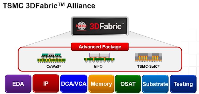
Currently the majority of high-end processors are monolithic, but design methodologies are slowly but surely shifting to multi-chiplet modules as leading-edge fabrication technologies get more expensive to use. In the coming years multi-chiplet system-in-packages (SiPs) are expected to become much more widespread, and advanced 2.5D and 3D chip packaging technologies will gain importance. To accelerate and simplify development of 3D designs, TSMC this week established its 3DFabric Alliance.


While multi-chiplet SiPs promise to simplify development and verification of highly complex designs, they require brand-new development methodologies as 3D packages bring a number of new challenges. This includes new design flows required for 3D integration, new methods of power delivery, new packaging technologies, and new testing techniques. To make the best use of the benefits of TSMC’s 2.5D and 3D packaging technologies (InFO, CoWoS, and SoIC), the chip development industry needs the whole ecosystem to work in concert on chiplet packaging – and this is what 3DFabric Alliance is designed to do.


“3D silicon stacking and advanced packaging technologies open the door to a new era of chip-level and system-level innovation, and also require extensive ecosystem collaboration to help designers navigate the best path through the myriad options and approaches available to them,” said Dr. L.C. Lu, TSMC fellow and vice president of design and technology platform.


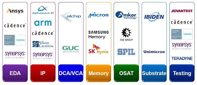
TSMC’s 3DFabric Alliance brings together developers of electronic design automation (EDA) tools, intellectual property providers, contract chip designers, memory manufacturers, advanced substrate producers, semiconductor assembly and test companies, and the groups making the equipment used for testing and verification. The alliance currently has 19 members, but over time it is expected to expand as new members join the group.


As the leader of the Alliance, TSMC will set certain ground rules and standards. Meanwhile members of 3DFabric Alliance will co-define and co-develop some of the specifications for TSMC’s 3DFabric technologies, will gain early access to TSMC’s 3DFabric roadmap and specs to align their plans with the foundry’s plans as well as those of other members of the alliance, and will be able to design and optimize solutions that are compatible with the new packaging methods. 


Ultimately, TSMC wants to ensure that members of 3DFabric Alliance will offer its clients compatible and interoperable solutions that will enable quick development and verification of multi-chiplet SiPs that use 2.5D and 3D packaging. 


For example, to unify the design ecosystem with qualified EDA tools and flows, TSMC has developed its 3Dblox standard. 3Dblox covers various aspects of building multi-chiplet devices featuring 2.5D and 3D packaging methodologies (such as chiplet and interface definitions), including physical implementation, power consumption, heat dissipation, electro-migration IR drop (EMIR), and timing/physical verification.


“Through the collective leadership of TSMC and our ecosystem partners, our 3DFabric Alliance offers customers an easy and flexible way to unlocking the power of 3D IC in their designs, and we can’t wait to see the innovations they can create with our 3DFabric technologies,” added Lu.


Ultimately, TSMC envisions that the alliance will greatly simplify and streamline the process for developing more advanced chips, especially for small and mid-size companies that rely more heavily on outside IP/designs. For example, if a company wants to develop a SiP consisting of logic chiplets stacked together and connected to an HBM3-based memory subsystem, EDA software from Ansys Cadence, Synopsys, and Siemens will allow it to design compatible chiplets, IP providers will sell those blocks the designer does not already have, TSMC will produce silicon, memory producers will offer compatible HBM3 KGSDs (known good stack dies), and then Ase Technology will assemble everything together. Meanwhile companies that do not have their own engineers will be able to order the design of the whole SiP (or individual chiplets) through Alchip or GUC, and then update their product over time if needed without needing to redesign everything, as the SiP will be built in accordance with 3DFabric and 3Dblox standards. 


3Dblox is currently supported by four major EDA developers. Eventually it will be supported by all members of the members if the alliance where needed.


While large companies like AMD and Nvidia tend to develop their own IP, interconnection, and packaging technologies, multi-chiplet SiPs promise to make the development of complex, chiplet-style processors accessible to smaller companies. For them, standard third-party IP, fast time-to-market, and proper integration are key to success, so 3DFabric Alliance and what it brings will be vital for them.


Source: TSMC


Source: AnandTech – TSMC Forms 3DFabric Alliance to Accelerate Development of 2.5D & 3D Chiplet Products

ONYX BOOX Tab Ultra ePaper Tablet Launches with Qualcomm Snapdragon 662

The e-Paper market has enjoyed steady growth over the last decade, starting with the introduction of the Amazon Kindle back in 2007. While there are many vendors attempting to make a mark in the technology required in this space, E-Ink’s offerings have ruled the roost.


The most popular category of products using E-Ink’s technology has undoubtedly been eBook readers. Recently, digital notebooks and notepads have also emerged as a significant driver in E-Ink’s expansion. These products take the regular e-reader and add support for an electronic pen / stylus. These products were initially quite expensive and targeted business professionals dealing with huge amounts of paperwork and requiring note-taking support (such as lawyers). The Sony DPT lineup (review) became one of the leading products in this category. As the market expanded, vendors such as reMarkable and ONYX also started putting out compelling products – expanding the target market to creative professionals and students as well. This category became truly mass-market a few months back with the introduction of Amazon’s Kindle Scribe (and slated to start shipping in time for the holiday season).


ONYX has been serving the e-reader market since 2006. They have an extensive lineup of e-readers (both grayscale and color), e-Paper tablets with note-taking support, and even E-Ink monitors. Today, the company is launching a new category – ePaper Tablet PCs. The first product in this lineup is the ONYX BOOX Tab Ultra – a 10.3″ unit complete with a 16MP rear-facing camera. A first for E-Ink devices, ONYX envisages the camera being used to OCR documents in the field without the need for an external device as an intermediary. The device targets professional use-cases. It must be noted that ONYX already carries the BOOX Note Air 2 Plus that carries most of the same features, but geared towards the home / casual consumer.


The ONYX BOOX Tab Ultra is the first e-reader model from ONYX to utilize the company’s proprietary fast refresh algorithm implemented using a separate hardware module on the board. The company has been using this on its Mira lineup of E-Ink monitors, and its use in the e-reader is supposed to improve user experience with web content. Scrolling, in particular, has been a weak point of E-Ink tablets due to the low refresh rate. The actual improvements delivered by the ONYX ‘BSR’ (BOOX Super Refresh) algorithm in this aspect needs hands-on evaluation for further analysis. The system supports four different modes for different tasks – reading books doesn’t require fast refreshing and can utilize the ‘HD Mode’, while typing requires a ‘Balance Mode’. A ‘Fast Mode’ is available for web browsing, and an ‘Ultrafast Mode’ for generic Android applications.


The BOOX Tab Ultra utilizes a Qualcomm Snapdragon 662 SoC (4x Kyro Gold (A73-class) @ 2GHz + 4x Kyro Silver (A53-class) @ 1.8 GHz, along with an Adreon 610 GPU), and comes with a specialized version of Android 11 (including Play Store support). The unit is equipped with a 6300 mAh battery, 4GB of LPDDR4x DRAM, and 128GB of eMMC flash storage. The USB-C port in the system also supports OTG functionality, and a micro-SDXC card slot. A keyboard case with a magnetic holder for the Tab Ultra is also available.


ONYX has a reputation for long support cycles, and provides regular firmware updates to augment the functionality of its ePaper tablets. Recent firmware updates have brought a more tablet-like experience in the user interface – a home screen with apps along with a favorites dock at the bottom. ONYX claims that the use of Android in its tablets (compared to custom OSes in other products such as the Kindle Scribe and reMarkable tablets) enables its customers to take advantage of the host of personal knowledge management apps available for note taking and data collection. Another recently added functionality relates to the association of different pages in different documents using easily-created tags.


The ONYX BOOX Tab Ultra is available for pre-order today and comes with a $600 price tag. The company is also simultaneously releasing the Nova Air 2 7.8″ e-Paper tablet with stylus support at $400 and the Leaf 2 7″ e-reader at $200. ONYX has typically not hesitated in trying out innovative ideas on the e-Paper front (they were one of the first vendors to bring out color e-readers), and equipping an e-reader / digital notebook with a rear camera is yet another interesting play from the company. The new products expand ONYX’s target market and build upon its position as one of the leading E-Ink product vendors in the market in the face of rising competition.


Source: AnandTech – ONYX BOOX Tab Ultra ePaper Tablet Launches with Qualcomm Snapdragon 662

AMD Announces Radeon RDNA 3 GPU Livestream Event for November 3rd

Following on the heels of AMD’s CPU-centric event back in August, AMD today has sent out a press release announcing that they will be holding a similar event in November for their Radeon consumer graphics business. Dubbed “together we advance_gaming”, the presentation is slated to be all about AMD Radeon, with a focus on the upcoming RDNA 3 graphics architecture and all the performance and power efficiency benefits it will bring. The event is set to kick off on November 3rd at 1pm ET (20:00 UTC), with undisclosed AMD executives presenting details.


Like the Ryzen event in August, next month’s Radeon event appears to be AMD gearing up for the launch of its next generation of consumer products – this time on the GPU side of matters. Back at the start of the summer, AMD confirmed that RDNA 3 architecture products were scheduled to arrive this year, so we have been eagerly awaiting the arrival of AMD’s next generation of video cards.


Though unlike AMD’s CPU efforts, the company has been far more mum about its next-gen GPU efforts. So details in advance on what will presumably be the Radeon RX 7000 series have been limited. The biggest items disclosed thus far are that AMD is targeting another 50% increase in performance-per-watt, and that these new GPUs (Navi 3x) will be made on a 5nm process (undoubtedly TSMC’s). Past that, AMD hasn’t given any guidance on what to expect for performance.


One interesting aspect, however, is that AMD has confirmed that they will be employing chiplets with this generation of products. To what extent, and whether that’s on all parts or just some, remains to be seen. But chiplets are in some respects the holy grail of GPU construction, because they give GPU designers options for scaling up GPUs past today’s die size (reticle) and yield limits. That said, it’s also a holy grail because the immense amount of data that must be passed between different parts of a GPU (on the order of terabytes per second) is very hard to do – and very necessary to do if you want a multi-chip GPU to be able to present itself as a single device.


We’re also apparently in store for some more significant upgrades to AMD’s overall GPU architecture. Though what exactly a “rearchitected compute unit” and “optimized graphics pipeline” fully entail remains to be seen.


Thankfully we should have our answer here in two weeks. The presentation is slated to air on November 29th at 1pm Pacific, on AMD’s YouTube channel. And of course, be sure to check out AnandTech for a full rundown and analysis of AMD’s announcements.


Source: AnandTech – AMD Announces Radeon RDNA 3 GPU Livestream Event for November 3rd

Intel Core i9-13900K and i5-13600K Review: Raptor Lake Brings More Bite

Today marks the release of Intel’s 13th Gen Core series, codenamed Raptor Lake. The first models to be unleashed into retail channels are all overclockable parts, with six SKUs across the Core i9, i7, and i5 product segments. While we’ve seen Intel’s heterogeneous or hybrid design with the launch of Intel’s Alder Lake (12th Gen Core) products, the latest Raptor Lake core brings a very similar design to the table, but with subtle improvements designed to help give Intel the leading edge in the desktop market.

First of these is a ‘new’ Raptor Cove performance (P) core using a refined Intel 7 manufacturing process with some subtle yet critical improvements to the LGA1700 platform to help increase generational performance. Perhaps the most significant benefit comes from adding more efficiency (E) cores, with the flagship SKU, the Core i9-13900K, bringing a total of 24-cores (8P+16E). Which means Intel has effectively doubled the number of efficiency cores on the die.

While there are plenty of talking points, ultimately, the proof, or in this case, performance, is in the pudding. With AMD pulling the trigger on its new Zen 4 core built on TSMC’s 5 nm process, does Intel’s 13th generation Core processors have what it takes to go toe-to-toe with the impressive Ryzen 7000? We aim to discover how Raptor Lake shapes up in our review of the Core i9-13900K and the more affordable Core i5-13600K.


Source: AnandTech – Intel Core i9-13900K and i5-13600K Review: Raptor Lake Brings More Bite

Intel Builds On USB4 v2 for 120 Gbps Next Generation Thunderbolt

The DisplayPort 2.1 specifications were officially released by VESA on Monday, and this was followed up by USB-IF’s announcement of the release of the 80 Gbps USB4 v2 specifications yesterday. These have have brought to fore the significant engineering efforts put into creating a unified protocol capable of handling the external I/O bandwidth requirements of tomorrow’s computing systems. Today, Intel is announcing the demonstration of early prototypes for next-generation Thunderbolt based on the USB4 v2 and DisplayPort 2.1 specifications.


Intel’s donation of the Thunderbolt 3 specifications to the USB promoters group to form the basis of USB4 has had its share of pros and cons. On one hand, the convergence of the Type-C connector ecosystem theoretically achieved the goal of minimizing end-user confusion, and the royalty-free spec for PCIe tunneling opened up the market to other silicon vendors like ASMedia. However, it also created consumer angst as most of the attractive features of USB4 (such as the 40Gbps bandwidth and compatibility with PCIe tunneling) were entirely optional features. That said, it did enable Intel to market Thunderbolt ports as the Type-C that could do it all. Intel’s demonstration of Next Generation Thunderbolt also included a sneak peek into its specifications, even though certain aspects are yet to be finalized. Before delving deeper into Intel’s press release, a quick recap of the 80 Gbps USB4 v2 specifications announcement is necessary.


USB4 v2 Updates


USB4 v2 builds upon the multi-protocol tunneling architecture introduced in USB4 by doubling the available bandwidth while maintaining the same port / pins layout and cable structure. This has been achieved by moving the physical layer signal encoding to PAM3 (described in detail in our coverage of 80 Gbps ‘Thunderbolt 5’ last year). This means that existing 40Gbps USB4 cables will be able to support 80Gbps operation also.


The USB4 v2 specifications now allow tunneling of DisplayPort 2.1 signals and up to four PCIe 4.0 lanes. The data and display protocol updates also make it more efficient, with USB data tunneling capable of exceeding 20 Gbps.


One of the key updates in the move to support DisplayPort 2.1 tunneling relates to the maximum total bandwidth for four lanes in UHBR 20 transmission mode. This translates to 80 Gbps, essentially leaving nothing spare on the transmit side for any other protocol. To handle this, USB4 v2 introduces the concept of asymmetric links. In general, a USB4 link uses two bonded high-speed differential signaling pairs to transmit and receive data, allowing for 40 Gbps duplex operation (40 Gbps transmit and 40 Gbps receive) in the symmetric case. However, the lane initialization process can optionally configure the link to have 3 transmitters and one receiver on one side, and 3 receivers and one transmitter on the other. Combined with the higher data rates thanks to PAM3, this can allow the host to send out 120 Gbps, while lowering the receive bandwidth to 40 Gbps. High-resolution displays can be reliably driven without too much of a sacrifice of the bandwidth available on the transmit side for other purposes (like high-speed storage).


The power delivery specifications have also been updated to match the updates made in USB4 v2, and new logo guidelines have been issued for consumer-facing equipment.


Next-Generation Thunderbolt


Thunderbolt has seen incredible momentum over the last couple of years – triggered mainly by the integration of Thunderbolt controllers inside the high-volume notebook processors starting with Ice Lake. The combination of data, video, and power delivery in one port / cable makes it beneficial to a host of use-cases. In particular, the increasing popularity of hybrid work / hot-desking (monitors / networking etc. behind a dock, allowing multiple employees to just plug in their Thunderbolt-equipped systems at different times) has also served as a fillip to Thunderbolt adoption in the business / office space. Gamers and content creators have an incredible thirst for I/O bandwidth that is served well by Thunderbolt.


As mentioned earlier, Next Generation Thunderbolt takes the USB4 v2 specifications as baseline and makes all of the attractive optional features into mandatory ones. On top of this, Intel’s integration of Thunderbolt into the notebook processors ensures that the implementation is power efficient on the host side. Making Thunderbolt mandatory for Intel Evo and vPro notebooks further cements Intel’s leadership in the USB4 v2 space.


The dynamic bandwidth rebalancing feature allowing tunneling of the highest bandwidth DisplayPort 2.1 streams while still allowing usage of high-bandwidth peripherals is one of the most exciting features of USB4 v2 that is sure to be available in systems equipped with the Next Generation Thunderbolt ports.


Intel’s demonstration included both host and device implementations, with the host configuration shown in the beginning. A discrete GPU’s DisplayPort output is fed into the host controller board, and two Type-C cables fork off, one ostensibly to the display, and another to a dock (device) with a SSD attached.


Aspects such as power delivery limits (Thunderbolt 3 / 4 support up to 15W by default) for the Next-Generation Thunderbolt ports will be clarified in the near future. Intel did not provide any information related to market availability.


Based on a glance through the USB4 v2 specifications and Intel’s description of Next-Generation Thunderbolt, it is clear that Thunderbolt ports will continue to remain the Type-C port that does it all.


Source: AnandTech – Intel Builds On USB4 v2 for 120 Gbps Next Generation Thunderbolt

NVIDIA Scrubs GeForce RTX 4080 12GB Launch; 16GB To Be Sole RTX 4080 Card

In a short post published on NVIDIA’s website today, the company has announced that it is “unlaunching” their planned GeForce RTX 4080 12GB card. The lowest-end of the initially announce RTX 40 series cards, the RTX 4080 12GB had attracted significant criticism since it’s announcement for bifurcating the 4080 tier between two cards that didn’t even share a common GPU. Seemingly bowing to the pressure of those complaints, NVIDIA has removed the card from their RTX 40 series lineup, as well as cancelling its November launch.


NVIDIA’s brief message reads as follows:


The RTX 4080 12GB is a fantastic graphics card, but it’s not named right. Having two GPUs with the 4080 designation is confusing.


So, we’re pressing the “unlaunch” button on the 4080 12GB. The RTX 4080 16GB is amazing and on track to delight gamers everywhere on November 16th.


If the lines around the block and enthusiasm for the 4090 is any indication, the reception for the 4080 will be awesome.


NVIDIA is not providing any further details about their future plans for the AD104-based video card at this time. However given the circumstances, it’s a reasonable assumption right now that NVIDIA now intends to launch it at a later time, with a different part number.


NVIDIA GeForce Specification Comparison
  RTX 4090 RTX 4080 16GB RTX 4080 12GB

(Cancelled)
CUDA Cores 16384 9728 7680
ROPs 176 112 80
Boost Clock 2520MHz 2505MHz 2610MHz
Memory Clock 21Gbps GDDR6X 22.4Gbps GDDR6X 21Gbps GDDR6X
Memory Bus Width 384-bit 256-bit 192-bit
VRAM 24GB 16GB 12GB
Single Precision Perf. 82.6 TFLOPS 48.7 TFLOPS 40.1 TFLOPS
Tensor Perf. (FP16) 330 TFLOPS 195 TFLOPS 160 TFLOPS
Tensor Perf. (FP8) 660 TFLOPS 390 TFLOPS 321 TFLOPS
TDP 450W 320W 285W
L2 Cache 72MB 64MB 48MB
GPU AD102 AD103 AD104
Transistor Count 76.3B 45.9B 35.8B
Architecture Ada Lovelace Ada Lovelace Ada Lovelace
Manufacturing Process TSMC 4N TSMC 4N TSMC 4N
Launch Date 10/12/2022 11/16/2022 Never
Launch Price MSRP: $1599 MSRP: $1199 Was: $899


Taking a look at the specifications of the cards, it’s easy to see why NVIDIA’s core base of enthusiast gamers were not amused. While both RTX 4080 parts shared a common architecture, they did not share a common GPU. Or, for that matter, common performance.


The RTX 4080 12GB, as it was, would have been based on the smaller AD104 GPU, rather than the AD103 GPU used for the 16GB model. In practice, this would have caused the 12GB model to deliver only about 82% of the former’s shader/tensor throughput, and just 70% of the memory bandwidth. A sizable performance gap that NVIDIA’s own figures ahead of the launch have all but confirmed.


NVIDIA, for its part, is no stranger to overloading a product line in this fashion, with similarly-named parts delivering unequal performance and the difference denoted solely by their VRAM capacity. This was a practice that started with the GTX 1060 series, and continued with the RTX 3080 series. However, the performance gap between the RTX 4080 parts was far larger than anything NVIDIA has previously done, bringing a good deal more attention to the problems that come from having such disparate parts sharing a common product name.


Of equal criticism has been NVIDIA’s decision to sell an AD104 part as an RTX 4080 card to begin with. Traditionally in NVIDIA’s product stack, 104 parts are used for the xx70 cards. And while video card names and GPU identifiers are essentially arbitrary, NVIDIA’s early performance figures painted a picture of a card that would have performed a lot like the kind of card most people would expect from the RTX 4070 – delivering performance upwards of 20% (or more) behind the better RTX 4080, and on-par with the last-generation flagship, the RTX 3090 Ti. In other words, there has been a great deal of suspicion within the enthusiast community that NVIDIA was attempting to sell what otherwise would have been the RTX 4070 as an RTX 4080, while carrying a higher price to match.


In any case, those plans are now officially scuttled. Whatever NVIDIA has planned for their AD104-based RTX 40 series card is something only the company knows at this time. Meanwhile come November 16th when the RTX 4080 series launches, the 16GB AD103-based cards will be the only offerings available, with prices starting at $1199.


Source: AnandTech – NVIDIA Scrubs GeForce RTX 4080 12GB Launch; 16GB To Be Sole RTX 4080 Card

Microsoft: DirectStorage 1.1 with GPU Decompression Finally on Its Way

As part of this week’s Microsoft Ignite developers conference, Microsoft’s DirectX team has published a few blog posts offering updates on the state of various game development-related projects. The biggest and most interesting of these is an update on DirectStorage, Microsoft’s API for enabling faster game asset loading. In short, the long-awaited 1.1 update, which adds support for GPU asset decompression, is finally on its way, with Microsoft intending to release the API to developers by the end of this year.


Source: AnandTech – Microsoft: DirectStorage 1.1 with GPU Decompression Finally on Its Way

The Iceberg Thermal IceSLEET G6 Stealth Review: Top-Tier Colossal Tower Cooler

In today’s review, we are taking a look at the flagship product of Iceberg Thermal, a relatively new US-based company. The IceSLEET G6 Stealth cooler that we are putting to the test today is a behemoth of a CPU cooler, intended to bring quiet cooling to users who want the very best but without the added complexity of liquid-based coolers.


Source: AnandTech – The Iceberg Thermal IceSLEET G6 Stealth Review: Top-Tier Colossal Tower Cooler

Micron Announces 20-Year Plan To Build $100 Billion U.S. Fab Complex

Now that the U.S. government has finally settled the matter of whether it would be providing subsidies to entice chip fabs to setup shop within the U.S., those fabs and chip makers are starting to hammer out their domestic investment plans. Of all of the proposals revealed so far, Micron’s new proposal stands to be the most ambitious. Last week the company announced plans to build the largest chip production complex in the history of the U.S. in central New York state. The plan will span 20 years of construction and upgrades, with a total price tag expected to hit around $100 billion by the time Micron is finished in the 2040s. 


Micron’s new site near Clay, New York, will not only be the company’s largest campus ever built, but will also be the largest chip fab in the USA. The new Micron campus will produce DRAM using leading-edge process technologies and is expected to eventually include four 600,000 feet2 (55,700 meters2) clean rooms. Which, to provide some context, is roughly eight-times the clean room space of GlobalFoundries’ Fab 8. The new fab complex will complement Micron’s already announced campus near Boise, Idaho, that is expected to start coming online starting in 2025. Both sites will be instrumental to meet Micron’s goal to produce 40% of its DRAM in the U.S. over the next decade.


According to Micron, the company’s investments in its New York production facility will total $100 billion when fully built, and it will create some 9,000 Micron jobs along with some 41,000 indirect jobs. The first phase of the Clay, New York, project is expected to cost Micron around $20 billion in total over the rest of this decade. The DRAM maker expects to get $5.5 billion in incentives from the state of New York over the life of the project, as well as federal grants and tax credits from the CHIPS and Science Act. In addition, Micron and the state of New York will also invest $500 million over the next 20+ years in community and workforce development.


Micron plans to start site preparation work in 2023 and start construction in 2024. The facility ramp up is set to begin in the second half of the decade based on industry demand for DRAM devices.


Broadly speaking, fab complexes with eye-popping price tags are quickly becoming the norm in the fab industry as the cost of building and equipping successive generations of fabs continues to balloon. And while Micron is not the first company to plan for a twelve digit price tag for a new fab complex (Intel’s new fab complex in Ohio is officially expected to cost around $100 billion when completed), Micron’s announcement is notable in that unlike Intel and TSMC, Micron isn’t a logic producer. So the company’s $100 billion plans are entirely for memory, a relatively bold commitment for a conservative company that’s competing in the tech industry’s classic commodity market.


Bearing in mind that the new fab in in Onondaga County, New York, is not set to come online until the later half of the decade, it is too early for Micro to reveal which process technologies and types of products it will produce. The only thing that the company says is that this will be a leading-edge facility that will produce advanced DRAM products (think 64Gb DDR5 chips, DDR6 DRAMs, next-generation HBM, etc.) using EUV-enabled production nodes.


“Micron will leverage the diverse, highly educated and skilled talent in New York as we look to build our workforce in the Empire State,” said Sanjay Mehrotra, chief executive of Micron. “This historic leading-edge memory megafab in Central New York will deliver benefits beyond the semiconductor industry by strengthening U.S. technology leadership as well as economic and national security, driving American innovation and competitiveness for decades to come.”


Source: Micron


Source: AnandTech – Micron Announces 20-Year Plan To Build 0 Billion U.S. Fab Complex

Samsung Foundry Outlines Roadmap Through 2027: 1.4 nm Node, 3x More Capacity

Samsung outlined its foundry business roadmap for the next five years at its Foundry Forum event last week. The company plans to introduce its next generation fabrication technologies in a timely manner and intends to make chips on its 1.4 nm (14 angstroms) manufacturing process by 2027. Also, the company will keep investing in new manufacturing capacity going forward as it strives to strengthen its position in the foundry market.


New Nodes Incoming


Samsung has been introducing new production nodes and/or variants on production nodes every 12 – 18 months for several years now, and plans to keep its rather aggressive pace going forward. Though the company’s roadmap illustrates, fanfare aside, that it is now taking longer to develop new fabrication processes. The company’s second-generation 3 nm-class gate-all-around (3GAP) technology is now set to arrive sometime in 2024. Meanwhile, Samsung Foundry intends to be ready with its 2 nm (20 angstroms) node in 2025, and with its 1.4 nm-branded fabrication process in 2027.


“With the company’s success of bringing the latest [3 nm-class] process technology to mass production, Samsung will be further enhancing gate-all-around (GAA) based technology and plans to introduce the 2 nm process in 2025 and 1.4 nm process in 2027,” a statement by Samsung reads.


  Chip Fab Roadmaps

Data announced during conference calls, events, press briefings and press releases
HVM Start 2023 2024 2025 2026 2027
Intel Process Intel 3 Intel 20A Intel 18A ? ?
  FET FinFET RibbonFET + PowerVia ? ?
  EUV 0.33 NA EUV 0.55 High-NA EUV
Samsung Process 3GAE 3GAP 2.0 nm 1.4 nm
  FET GAAFET ? ? ?
  EUV 0.33 NA EUV ? ? ?
TSMC Process N3E/N3P N3S/N3X N2 N2?  
  FET FinFET GAAFET GAAFET with backside power delivery (?)
  EUV 0.33 NA EUV ? ? ?


Painting some very broad strokes, compared to those of Intel and TSMC, it seems like TSMC is a little bit more conservative (which is something expected when you are the world’s largest contrast maker of microelectronics). Whereas Intel is more aggressive (which is again expected given the company’s position in the market of semiconductors). Meanwhile, naming of fabrication processes these days is essentially aspiratory, with little connection to their real physical measures. Which is why comparing different semiconductor companies’ roadmaps is an imprecise metric at best.


In addition to new ‘general’ nodes, Samsung plans to expand its process technology optimization programs for each specific application as well as customized services for customers, the company said.


Meanwhile, one of the things that Samsung notably did not mention in its press release concerning its 1.4 nm node is usage of High-NA equipment. Intel, for its part, plans to use High-NA starting its Intel 18A node (in 2024), where it will eventually be supplanting the EUV multi-patterning used on initial 18A production. 


According to Samsung, the adoption of new process technologies and demand for new fabrication processes will be driven by already known mega trends — AI, autonomous vehicles, automotive applications in general, HPC, 5G, and eventual 6G connectivity. Keeping in mind that Samsung is a large industrial conglomorate with many divisions, many of applications that it intends to address with future process nodes are its own.


The company disclosed last week that its LSI Business (chip development division) currently offers around 900 products, which include SoCs, image sensors, modems, display driver IC (DDI), power management IC (PMIC), and security solutions. Going forward the company plans to put even more efforts into development of performance-demanding IP, including CPU and GPU, by working closer with its industry partners (which presumably includes Arm and AMD).


Expanded Production Capacity


Offering state-of-the-art production technologies is good, but to produce those advanced chips in sufficient quantities to meet market demands is equally important. To that end, Samsung announced that the company will also continue to invest heavily into building out additional production capacity. In the recent years Samsung’s semiconductor capacity CapEx was around $30 billion a year and it does not look like the firm plans to put a cap on its spendings (though it is noteworthy that it does not disclose how much money it intends to spend).


Samsung plans to expand its production capacity for its ‘advanced’ process technologies by more than three-fold by 2027. While the companies is not naming the nodes it considers “advanced”, we would expect a significant addition of its EUV capacity in the next five years – especially as more ASML EUV machines become available. Meanwhile, the company will adopt ‘Shell-First’ tactics in its expansion and construct buildings and clean rooms first, and add equipment later on depending on market conditions.


Samsung’s new fab under construction near Taylor, Texas, will be one of the company’s main vehicles to add capacity in the coming years. The shell-first site will start to produce chips in 2024. And as the company adds new tools to the fab and build new phases, production capacity of the site will further increase. 


Source: Samsung


Source: AnandTech – Samsung Foundry Outlines Roadmap Through 2027: 1.4 nm Node, 3x More Capacity

AMD Issues Early Q3’22 Financial Results: Misses Guidance By $1B as Client Revenue Craters

Underscoring a difficult second half of the year that seems to be shaping up for the entire tech industry, AMD this afternoon has become the latest tech company to warn investors that revenues for the quarter are going to come in significantly under previous guidance. Releasing a preliminary third quarter financial results statement, AMD is reporting that revenues for the quarter will come in at around $5.6 billion, which is over $1 billion below AMD’s previous guidance of $6.7 billion. Driving this unexpected drop in revenues is an exceptionally weak client market, with revenues down 40% versus Q3’21 and resulting in what’s traditionally AMD’s largest market segment by revenue becoming their smallest.


Source: AnandTech – AMD Issues Early Q3’22 Financial Results: Misses Guidance By B as Client Revenue Craters

SanDisk Professional PRO-G40 Thunderbolt / USB Dual-Mode Portable SSD Review

Western Digital is introducing a new flagship portable SSD today under the SanDisk Professional brand. The PRO-G40 dual-mode PSSD ticks all the right boxes for prosumers, content creators, and studios looking for a high-performance rugged bus-powered portable storage drive with wide compatibility. We have put the 2TB version of the PRO-G40 through our rigorous direct-attached storage evaluation. Read on to find out how the new PSSD stacks up against the competition.


Source: AnandTech – SanDisk Professional PRO-G40 Thunderbolt / USB Dual-Mode Portable SSD Review

Intel Demos Sapphire Rapids Hardware Accelerator Blocks In Action At Innovation 2022

With Intel’s annual Innovation event taking place this week in San Jose, the company is looking to recapture a lot of technical momentum that has slowly been lost over the past couple of years. While Intel has remained hard at work releasing new products over the time, the combination of schedule slips and an inability to show off their wares to in-person audiences has taken some of the luster off the company and its products. So for their biggest in-person technical event since prior to the pandemic, the company is showing off as much silicon as they can, to convince press, partners, and customers alike that CEO Pat Gelsinger’s efforts have put the company back on track.

Of all of Intel’s struggles over the past couple of years, there is no better poster child than their Sapphire Rapids server/workstation CPU. A true next-generation product from Intel that brings everything from PCIe 5 and DDR5 to CXL and a slew of hardware accelerators, there’s really nothing to write about Sapphire Rapids’ delays that hasn’t already been said – it’s going to end up over a year late.

But Sapphire Rapids is coming. And Intel is finally able to see the light at the end of the tunnel on those development efforts. With general availability slated for Q1 of 2023, just over a quarter from now, Intel is finally in a position to show off Sapphire Rapids to a wider audience – or at least, members of the press. Or to take a more pragmatic read on matters, Intel now needs to start seriously promoting Sapphire Rapids ahead of its launch, and that of its competition.

For this year’s show, Intel invited members of the press to see a live demo of pre-production Sapphire Rapids silicon in action. The purpose of the demos, besides to give the press the ability to say “we saw it; it exists!” is to start showing off one of the more unique features of Sapphire Rapids: its collection of dedicated accelerator blocks.

Along with delivering a much-needed update to the CPU’s processor cores, Sapphire Rapids is also adding/integration dedicated accelerator blocks for several common CPU-critical server/workstation workloads. The idea, simply put, is that fixed function silicon can do the task as quickly or better than CPU cores for a fraction of the power, and for only a fractional increase in die size. And with hyperscalers and other server operators looking for big improvements in compute density and energy efficiency, domain specific accelerators such as these are a good way for Intel to deliver that kind of edge to their customers. And it doesn’t hurt either that rival AMD isn’t expected to have similar accelerator blocks.


Source: AnandTech – Intel Demos Sapphire Rapids Hardware Accelerator Blocks In Action At Innovation 2022

NZXT Unveils N7 Z790 Motherboard for Intel 13th Gen Core Series

With a lot of news and info dropping on Intel’s latest Z790 chipset using the LGA1700 socket, NZXT has pulled the trigger and announced its N7 Z790 motherboard. Available in either white or black, it features a 2.5 GbE controller, Wi-Fi 6E CNVi, benefits from support for PCIe 5.0, and includes three M.2 slots.


In addition to the announcement of Intel’s 13th Gen Core series processors, codenamed Raptor Lake, NZXT has announced its plans to launch the N7 for Z790. As we’ve seen from NZXT motherboards in the past, the N7 Z790 has a large swathe of armor covering the board and is available in both back and white color schemes. It should be noted that neither the black nor white model includes any integrated RGB LED lighting. Typical with an NZXT product, the N7 Z790 comes with support with their CAM software.


Some of the NZXT N7 Z790’s main features include one full-length PCIe 5.0 x16 slot, two full-length PCIe 4.0 slots operating at x4/x4, and two PCIe 3.0 x1 slots. Also present on the NZXT N7 Z790 are three M.2 slots, two with support for PCIe 4.0 x4 NVMe drives and one with support for both PCIe 4.0 x4 and SATA. NZXT also includes four SATA ports with support for RAID 0, 1, 5, and 10 arrays for more conventional storage. NZXT is also advertising support for DDR5-6000 memory, with a combined total of 128 GB supported across four slots.


NZXT is also advertising a 16+1+2-phase power delivery, with one 8-pin EPS 12 V and one 4-pin 12 V power connector pairing to deliver power to the CPU. Powering the rest of the board’s components is a 24-pin 12V power connector.


The rear I/O is modest yet practical, with two USB 3.2 G2 Type-A and three USB 3.2 G1 Type-A; interestingly, NZXT doesn’t include any rear panel Type-C connectivity. Also on the rear panel are five 3.5 mm audio jacks and one S/PDIF optical output powered by a Realtek ALC1220 HD audio codec, with two antenna ports for an unspecified Wi-Fi 6E CNVi. Finishing off the rear panel is a single HDMI TM video output, with one Realtek RTL8125BG 2.5 GbE controller.


The NZXT N7 Z790 is scheduled to release with an MSRP of $300 and will be available in Q4 2022 in the USA. NZXT hasn’t shared whether or not this will be released in other regions.


Source: NZXT


Source: AnandTech – NZXT Unveils N7 Z790 Motherboard for Intel 13th Gen Core Series

Intel Innovation 2022 Keynote: Live Blog (9am PT, 4pm UTC)

It’s time again for another Intel event, Intel Innovation 2022. With plenty of tech things to reveal to the world ranging from AI, client computing, and data center/cloud computing. Intel is also expected to showcase the generation of products for consumers.


With AMD’s big Ryzen 7000 launch having only taken place just yesterday, Intel is expected to showcase its next generation of products for consumers. Leading the keynote will be visionary Intel CEO Pat Gelsinger.


The live blog will start with the opening keynote from Intel Innovation at 9am PT / 16:00 UTC / 18:00 CEST.


Source: AnandTech – Intel Innovation 2022 Keynote: Live Blog (9am PT, 4pm UTC)

Netgear Introduces Wi-Fi 6 / 6E Access Points and Services for Residential Installers

Netgear has been at the forefront of the SDVoE (Software-Defined Video over Ethernet) initiative with multiple AV switches serving the growing market. The ProAV lineup of managed switches have been sold primarily in a B2B setting by the Netgear Business division. These switches are increasingly becoming part of luxury residential installations requiring an AV-over-IP solution. As part of the CEDIA Expo 2022, Netgear is announcing a new ‘Netgear Home Solutions’ push. The intention is to take the same lineup of Netgear AV products sold by Netgear Business and target it towards both commercial and residential installations.


As part of this initiative, Netgear will be selling ProAV Managed Switches and ProWiFi Access Points to residential installers, along with the Pro version of Insight Remote Management and Pro Support. While the ProAV Managed Switches are already in the market, the new WAX628 and WAX638E APs are complementary to the currently existing members of the Insight Access Point Portfolio.


The WAX628 (already available for residential installers) slots in-between the dual-band AX3600 WAX620 and the tri-band AX6000 WAX630. This AX5400 dual-band solution supports 160 MHz channel bandwidth, and is accompanied by the AX7800 WAX638E which adds 6 GHz band support to the mix. The Wi-Fi 6E AP is slated to come to the market in the next few months.


Netgear is promising margin protection for installers by selling the ProAV and ProWiFi products only through the channel and not via Amazon or other e-tailers. Since these products are going to reach end-consumers through custom installers who have their own cost structures, the lack of any pricing information from Netgear is not surprising.


Netgear’s traditional consumer Wi-Fi router market has evolved rapidly over the last few years. Despite the success of Orbi (in both the consumer and SMB markets), new entrants like eero have gained significant mind and market share. In this context, Netgear has to look towards services and expand into new markets in order to maintain and build upon their technical leadership. Forays into lucrative niches like the residential installer market are not surprising.


Source: AnandTech – Netgear Introduces Wi-Fi 6 / 6E Access Points and Services for Residential Installers