AMD Unveils Ryzen 9 7950X3D, 7900X3D, and Ryzen 7 7800X3D, Up to 128 MB of L3 Cache And 5.7 GHz Boost

During Computex 22, AMD showcased its updated CPU roadmap going through 2024, which yielded some exciting propositions to the desktop processor market. One of those products highlighted was a new 3D V-Cache SKU based on Zen 4 cores, and with the success of its previous Ryzen 7 5800X3D with 96 MB of 3D stacked V-Cache, gamers have been chomping at the bit for more ever since. Using their primetime keynote slot during CES 2023, AMD has unveiled its next 3D V Cache-based processors to the market using its Zen 4 core architecture.


AMD hasn’t unveiled just one new Zen 4-based X3D SKU; it’s announcing three across the Ryzen 7000 series, the Ryzen 9 7950X3D, the Ryzen 9 7900X3D, and the Ryzen 7 7800X3D. Aside from 64 MB of additional L3 cache through AMD’s 3D V-Cache stacking technology, which is a 3D chiplet stacking technology in conjunction with TSMC, all three Zen 4 X3D SKUs feature a 120 W TDP. They also have higher boost core frequencies than previous X3D chips, with the Ryzen 9 7950X3D boosting up to an impressive of 5.7 GHz on the core.


Source: AnandTech – AMD Unveils Ryzen 9 7950X3D, 7900X3D, and Ryzen 7 7800X3D, Up to 128 MB of L3 Cache And 5.7 GHz Boost

AMD Lays Out 2023 Ryzen Mobile 7000 CPUs: Top-to-Bottom Updates, New Zen 4 'Phoenix' CPU Takes Point

This year’s CES has turned out to be a laptop-centric event in the PC space, and no farther do you have to look for proof of that than AMD’s CES keynote. The densely packed keynote immediately kicked things off with the announcement of AMD’s 2023 mobile product stack, which will see the CPU vendor mixing and matching silicon across multiple generations of designs to put together a fresh product stack for the new year. This includes the return of some old favorites, including bringing desktop Zen 4 silicon to mobile, as well as the introduction of AMD’s brand-new Phoenix CPU silicon, their first mobile-focused Zen 4 CPU design.


Source: AnandTech – AMD Lays Out 2023 Ryzen Mobile 7000 CPUs: Top-to-Bottom Updates, New Zen 4 ‘Phoenix’ CPU Takes Point

AMD Announces Ryzen Mobile 7045 HX-Series CPUs, Up to 16-Cores and 5.4 GHz for Laptops

While many companies such as Razer offer ‘desktop’ replacements in the form of very high-end and powerful gaming laptops, the silicon that goes into them not only needs to deliver similar levels of performance but it’s got to be efficient too. With high-end mobile processors coming out at least once a year, during their opening keynote at CES 2023, AMD CEO Dr. Lisa Su unveiled the latest in AMD’s Ryzen mobile products for the high-end laptop space, the Ryzen 7045HX-series.


Leading the charge is the AMD Ryzen 9 7945HX with 16-cores and 32-threads and an incredible boost frequency of 5.7 GHz, all under a configurable TDP of 55-75 W+. AMD has three other Ryzen 7045HX-series processors, including the Ryzen 9 7845HX, a 12-core/24-thread part, the Ryzen 7 7745HX, and the AMD Ryzen 5 7645HX. With a loaded four-SKU stack ranging from 16-cores down to 6-cores, AMD has high-performance mobile parts for all manors of gaming notebooks and high-performance laptops.


Source: AnandTech – AMD Announces Ryzen Mobile 7045 HX-Series CPUs, Up to 16-Cores and 5.4 GHz for Laptops

The AMD CES 2023 Keynote Live Blog (6:30pm PT/02:30 UTC)

CES keynote season continues this week with the second major PC-centric keynote of the event, being held by AMD. Helmed as always by CEO Dr. Lisa Su, AMD is taking the center stage this evening to share their plans and products for consumer electronics for 2023. AMD is in the midst of rolling out their Zen 4 CPU architecture and RDNA 3 GPU architecture across their product lines, so there’s ample space in both AMD’s desktop and mobile product lineups to introduce some new parts – and we don’t expect to come away empty-handed.

Come join us at 6:30pm PT / 7:30pm ET / 02:30 UTC to get all the details.


Source: AnandTech – The AMD CES 2023 Keynote Live Blog (6:30pm PT/02:30 UTC)

ASRock Industrial's NUC(S) 1300 BOX Series Brings Raptor Lake to UCFF Systems

Intel recently updated their low-power processors lineup with the Raptor Lake U- and P- Series 13th Gen Core mobile SKUs. Supporting a range of TDPs up to 28W, these SKUs allow ultra-compact form-factor (UCFF) PC manufacturers to update their traditional NUC clones. Starting with Tiger Lake, ASRock Industrial took over ASRock’s Beebox chassis design and equipped it with a 4″x4″ industrial PC motherboard internally. The company has typically announced these NUC clones within a few days of Intel’s platform announcement, and things are no different with Raptor Lake this time around.


One of the key updates this time around is the bifurcation of the NUC BOX lineup into slim and high-rise versions – the traditional NUC 1300 BOX series retains the previous industrial design with support for a 2.5″ SATA drive. The new NUCS 1300 BOX series forsakes the 2.5″ drive support and cuts down the height of the system from 47.85mm to 38mm. The company is also currently restricting the processor choice to either the Core i7-1360P or Core i5-1340P. In total, there are six different models being launched, and the key differences are summarized in the table below. Dual LAN capabilities are available only in the high-rise versions.


ASRock Industrial NUC(S) 1300 BOX (Raptor Lake-P) Lineup
Model NUCS BOX-13xxP/D4 NUC BOX-13xxP/D4 NUC BOX-13xxP/D5
CPU xx:60 Intel Core i7-1360P

4P + 8E / 16T

(P) 2.2 – 5.0 GHz

(E) 1.6 – 3.7 GHz

28W – 64W
xx:40 Intel Core i5-1340P

4P + 8E / 16T

(P) 1.9 – 4.6 GHz

(E) 1.4 – 3.4 GHz

28W – 64W
GPU xx:60 Intel® Iris Xe Graphics (96EU) @ 1.5 GHz
xx:40 Intel® Iris Xe Graphics (80EU) @ 1.45 GHz
DRAM Two DDR4 SO-DIMM slots

Up to 64 GB of DDR4-3200 in dual-channel mode
Two DDR5 SO-DIMM slots

Up to 64 GB of DDR5-4800 in dual-channel mode
Motherboard 4.02″ x 4.09″ UCFF
Storage SSD 1x M.2-22(42/60/80) (PCIe 4.0 x4 (CPU-direct))
DFF 1 × SATA III Port (for 2.5″ drive)
Wireless Intel Wi-Fi 6E AX211

2×2 802.11ax Wi-Fi (2.4Gbps) + Bluetooth 5.2 module
Ethernet 1 × 2.5GbE port (Intel I226-LM) 2 × 2.5GbE port (Intel I226-LM)
USB Front 2 × USB 3.2 Gen 2 Type-A

1x USB4 (Thunderbolt 4-capable, DP 1.4a Alt Mode)

1x USB 3.2 Gen 2 Type-C with DP 1.4a Alt Mode
1 × USB 3.2 Gen 2 Type-A

1x USB4 (Thunderbolt 4-capable, DP 1.4a Alt Mode)

1x USB 3.2 Gen 2 Type-C with DP 1.4a Alt Mode
1 × USB 3.2 Gen 2 Type-A

1x USB4 (Thunderbolt 4-capable, DP 2.1 Alt Mode)

1x USB 3.2 Gen 2 Type-C with DP 1.4a Alt Mode
Rear 2 × USB 3.2 Gen 2 Type-A
Display Outputs 2 × HDMI 2.0b (Rear)

2 × DisplayPort 1.4a (using Front Panel Type-C ports)
1 × HDMI 2.0b (Rear)

1 x DisplayPort 1.4a (Rear)

2 × DisplayPort (using Front Panel Type-C ports)
Audio 1 × 3.5mm audio jack (Realtek ALC233) 1 × 3.5mm audio jack (Realtek ALC256)
PSU External (19V/90W)
Dimensions Length: 117.5 mm

Width: 110 mm

Height: 38 mm
Length: 117.5 mm

Width: 110 mm

Height: 47.85 mm


Note that the M.2 2280 support in the NUC BOX is enabled with a separate bracket, while the screw base is already at the correct position in the NUCS BOX.


Similar to the NUC 1100 and NUC 1200 BOX series units, one of the Type-C ports in the front panel is advertised as USB4, but does possess Thunderbolt 4 capabilities. ASRock Industrial seems to have retained the same components from the NUC 1200 BOX series for the NUC(S) BOX 1300/D4 series too – so, while the port is USB4 and has 40Gbps capabilities along with DP 1.4a Alt Mode, it doesn’t have the newly advertised 20G (USB 3.2 Gen 2×2) support that Intel has promised for the Thunderbolt ports in the low-power Raptor Lake mobile platforms. One of the requirements for this support seems to be the new Hayden Bridge retimer, which is not used in the NUC(S) 1300 BOX/D4 series.


However, it does look the DDR5-capable D5 version uses a different configuration, allowing it to claim DP 2.1 from the USB4 port. We have reached out to ASRock Industrial to check if this enables 20G USB 3.2 Gen 2×2 support also.


In terms of availability and pricing, the company plans to release the DDR4 version first. The NUCS 1300/D4 BOX Series will ship early next month, while the NUC 1300/D4 Series with SATA support will ship towards the middle of February. The barebones 1360P versions of both systems (without the SODIMMs and disk drive(s)) is expected to have a market price of around $700.


Source: AnandTech – ASRock Industrial’s NUC(S) 1300 BOX Series Brings Raptor Lake to UCFF Systems

CES 2023: HP Unveils Dragonfly G4 Notebook for Business

During CES 2023 in Las Vegas, HP announced the latest entry to its Dragonfly notebook series, the Dragonfly G4. Catering to SMIBs and business use in general, HP states it’s the world’s first business notebook to support the simultaneous use of dual cameras. It also comes equipped with Intel’s latest 13th Gen Mobile processor and HP Fast Charge support that can charge the G4 up to 50% battery in just 30 minutes.


With numerous features on offer, HP’s latest Dragonfly entrant, the G4, has been updated for 2023 with the inclusion of Intel’s latest 13th Generation mobile processors. The HP Dragonfly G4 has various configurations, including a svelte 90% recycled magnesium alloy chassis, starting with a weight of just 2.2 lbs. However, depending on the configuration, it could weigh slightly more.


HP Dragonfly G4 in Slate Blue


Touching on some of the finer specifications, the HP Dragonfly G4 can be configured to support up to 32 GB of soldered LPDDR5 memory. However, memory support depends solely on the processor, and HP hasn’t shared which of Intel’s 13th Gen mobile line-ups will be featured. Regarding storage, users can have up to 2 TB of PCIe 4.0 x4 M.2 storage. At the same time, the 13.5-inch diagonal (3:2) display can be configured with a 400-nit WUXGA+ screen, a 1000-nit Sure View Reflect panel, or a 3K2K OLED 400-nit display, and available in both touchscreen and non-touch variants.


HP also supports Intel’s Wi-Fi 6E wireless interface with BT 5.2 and a decent selection of connectivity, including dual Thunderbolt 4 Type-C connectors, one USB 5 Gbps Type-A, and one HDMI 2.0 video output for external displays. The HP Dragonfly G4 also comes with HP Fast Charge support, HP Power Management with Smart Sense, Wolf Security, and many more security iterations provided by HP.


Touching more on HP’s claim that the HP Dragonfly G4 is the world’s first business notebook to support the use of dual cameras at the same time, HP also states that the second camera is sold separately or as an optional feature and also requires the myHP application to work as intended.


The HP Dragonfly G4 is expected to be available sometime in Spring in either a Slate Blue or Natural Silver colored finish. Pricing and a complete list of specifications are expected closer to its launch.


Source: HP


Source: AnandTech – CES 2023: HP Unveils Dragonfly G4 Notebook for Business

CES 2023: Plugable Introduces New Flagship Thunderbolt 4 Dock and USB-C Hub

The Thunderbolt and USB ecosystems have seen rapid updates over the last couple of years. In 2022, we saw the announcement of the USB4 v2 standard and some details of Next Generation Thunderbolt with total bidirectional speeds of up to 160 Gbps (80 Gbps TX / RX with symmetric links, and 120 Gbps TX / 40 Gbps RX using asymmetric links from the host perspective). Product introductions have typically lagged behind the announcement of the standards by 18 – 24 months, and we are currently in the midst of the introduction of the second wave of Thunderbolt 4 and USB4 products.


At CES 2023, Plugable is introducing its first Thunderbolt 4 dock – the TBT4-UDZ. One of the key updates in Thunderbolt 4 was the bridging of features common in the USB world. Consequently, the first-generation products were focused on delivering the newly introduced hub functionality to users. Plugable had launched the highly appreciated TBT4-HUB3C back in September 2021 to cover that aspect. The TBT4-UDZ being announced today is a flagship dock equipped with the Intel Goshen Ridge controller. It provides 16 additional ports and host charging up to 100W. There are four additional display outputs (2x HDMI 2.0 + 2x Display Port 1.4), though the number of actual displays that can be driven depends on the host’s capabilities.


The 2.5 Gbps NBASE-T port is a welcome addition to the feature set of Thunderbolt docks. It is something that we are seeing in most of the newly-launched Thunderbolt 4 docks from different vendors. Despite the presence of a large number of useful ports, a downstream Thunderbolt port is conspicuous by its absence. Though this dock can be connected to one of the Thunderbolt 4 ports in the TBT4-HUB3C, it might be interesting from a technical perspective to combine both hub and dock functionality into a single device.


Plugable is planning to start shipping the TBT4-UDZ on January 17th, with pre-orders for $299 already active on Amazon.


The USBC-11IN1E is Plugable’s flagship USB-C hub, and a follow-up to the USBC-7IN1E introduced in 2020 and updated in 2021 with newer internals and I/Os. The additional ports do add to the price – the 11-port version is priced at $79, compared to the $40 of the 7-port version.


The hub requires the host’s USB-C port to support MST on the DP Alt Mode output to enable both HDMI ports. Without MST, usage of the DP Alt Mode results in the mirroring of the display outputs. The hub retains the USB-C power input (to which the notebook’s original charger can be connected for passthrough charging).


Plugable is also adding 1m (3.3ft) Thunderbolt 4 and USB4 passive cables to its product portfolio. The new cables support 40 Gbps speeds and 240W charging (Extended Power Range). The Thunderbolt-certified TBT4-240W-1M is priced at $29.25, while the USB-IF-certified USB4-240W-1M is priced at $25.95. The price difference seems solely due to the difference in certification costs – it is likely that the USB-IF certified cable will work just as well with Thunderbolt 4 setups.


Source: AnandTech – CES 2023: Plugable Introduces New Flagship Thunderbolt 4 Dock and USB-C Hub

Intel Announces Gracemont-based N-Series Processors For Entry-Level Mobile and Systems

Although Intel’s 13th Gen Core mobile announcement tends to steal the limelight away from many of its other product announcements, Intel has also announced four new SKUs from its N-series of processors. Representing the entry-level, Intel’s latest N-series processor for mobile and desktop (codenamed Alder Lake-N), replacing Intel’s Tremont architecture-based Jasper Lake platform. Alongside up to 8 CPU cores, these new low-end SoCs include Wi-Fi 6E connectivity, GNA 3.0 background noise suppression, and integrates IPU and MIPI camera support rolled into one solution. This makes it a suitable series of products designed for video conferencing and high-end wireless connectivity for entry-level notebooks, Chromebooks, and low-power users.


Based around the same Gracemont CPU microarchitecture Intel uses for efficiency (E) cores in its 12th and 13th Gen Core processors, Intel’s N-Series processors are designed for low-powered and affordable slimline notebooks and desktops, where efficiency is vital. Intel is also claiming double-digit performance gains with the latest quad-core Intel Inside N200 processor compared to the previous series, with 28% better overall application performance and up to 28% gains in web browsing performance.


Stepping up to the Core i3 N-series processors, Intel is claiming gains of up to 42% in overall application performance, which is advantageous from an efficiency and performance per watt perspective. Not only is the N-series the entry-level processors designed for budget Windows notebooks and Chromebooks, but Intel’s claims look to surpass its previous Jasper Lake models, such as the N6000, out of the water. With either eight or four Gracemont cores, the same efficiency (E) core is used in Intel’s 13/12th Gen Core series families.


Regarding features, Intel has plenty up its sleeve as it promises advantageous video conferencing capabilities due to its integral Image Processing Unit (IPU) and MIPI camera interface, along with dynamic noise suppression for microphones. With noise suppression handy for video conference calls and eliminating background noise, it uses a low-powered Gaussian and Neural Accelerator (GNA 3.0) technology to achieve this.


Focusing on connectivity, the N-series can accommodate up to four USB 3 and eight USB 2 and has nine PCIe 3.0 lanes available for devices and controllers. By proxy, the Intel N-series now also benefits from Intel’s WI-Fi 6E CNVi with BT 5.2 device connectivity, along with USB 3.2 Gen 2 and DisplayPort 1.4 support.


Intel N300/200-Series (Gracemont Core on Intel 7)
AnandTech Cores

C/T
E-Core

Base
E-Core

Turbo
L3 Cache

(MB)
Processor

Graphics
Memory

Support
Turbo

W
i3-N305 8/8 ? 3800 6 32 EU DDR5-4800

DDR4-3200
15
i3-N300 8/8 ? 3800 6 32 EU DDR5-4800

DDR4-3200
7
 
IP N200 4/4 ? 3700 6 32 EU DDR5-4800

DDR4-3200
6
IP N100 4/4 ? 3400 6 24 EU DDR5-4800

DDR4-3200
6


The Core i3 N-series CPUs come with eight cores and eight threads, versus the four cores and four threads of the Intel Processor N200 and N100 chips. The Core i3-N305 is the top-tier SKU for the entry-level series, with eight Gracemont cores that can turbo up to 3.8 GHz and a maximum turbo TDP of 15 W. Memory support is similar to its 13th Gen Core family with DDR5-4800, LPDDR5-4800, and DDR4-3200 support across all four SKUs.


The Core i3-N300 has similar specifications, including 32 EU graphics cores and 6 MB of L3 cache, but with just over half the power budget available with a maximum turbo TDP of 7 W. Focusing on the two entry-level Intel Processor branded chips, the IP-N200 and IP-N100 both include four Gracemont cores and four threads, along with 6 MB of L3 cache. Both feature a turbo TDP of 6 W, although the IP-N200 hs an E-core turbo of 3.7 GHz, with 32 EU graphics core units, while the entry-level N100 has a maximum clock speed of 3.4 GHz and just 24 EU graphics cores.


Intel has specified that it has over 50 OEM designs ready to go with its N-series processors, including partnerships with Windows OEMs such as HP, ASUS, and Lenovo, as well as partnerships with ChromeOS and leading Chromebooks. It hasn’t been stated when the N-series will start filtering into retail models, but this is expected to be soon.


Source: AnandTech – Intel Announces Gracemont-based N-Series Processors For Entry-Level Mobile and Systems

Intel Unveils 13th Gen Core Mobile Processors: Raptor Lake-HX, H, P, and U Series, Up To 24 Cores

Not just focused on their new 13th gen Core desktop chips, Intel this morning is also kicking off 2023 for its mobile customers in a big way with the announcement of the 13th generation Core mobile family. Based on the same Raptor Lake architecture as Intel’s 13th gen Core desktop chips, Intel is launching (or at least, announcing) the full 13th gen mobile stack all in one go. This means everything from the ultra-portable U-series chips up to the desktop replacement-class HX-series. All of them gaining Raptor Lake’s CPU architectural enhancements, along with a smattering of new features that are coming to the overall platform.

Leading the lineup – and first SKUs out the door – are the 13th generation Core HX-series processors for high-performance notebooks. With SKUs featuring up to 24 CPU cores (8P+16E), Intel is looking to deliver desktop-level performance in the mobile space, with turbo clock speeds of up to 5.6 GHz, a turbo TDP of 157 W, and a base TDP of 55 W. Like previous iterations of the HX series, these parts are based on Intel’s desktop silicon (Raptor Lake-S), so they are designed to be placed in DTR-class laptops and are almost always paired with a discrete GPU.

Also being announced today are the enthusiast-level H-series processors, Intel’s more traditional mobile-optimized processors for high performance laptops. These offer fewer cores and slightly lower clockspeeds than the HX processors, but are better suited for mobile operation with a more powerful integrated GPU and support for technologies like LPDDR5 memory. Finally, joining the H-series will be Intel’s thin and light performance-based P-series chips, and their U-series (ultrathin) chips use in the most portable of laptops, making the usual power/performance tradeoffs to get Raptor Lake in increasingly light laptops.

As was the case with Intel’s Raptor Lake desktop parts, their 13th gen Core mobile parts are largely a drop-in replacement for their previous-generation Alder Lake processors. This means that Intel’s army of OEM partners are going to be hitting the ground running with laptops incorporating the new chips – and CES will be awash in new laptop announcements. All told, Intel has an exntesive lineup of SKUs on offer, benefiting from its Intel 7 node and hybrid architecture of performance (P) and efficiency (E) cores. There’s a whole stack of Raptor Lake mobile processors for every price point and requirement, from high-end gaming to portable workstation levels, as well as run-of-the-mill entry-level notebooks for users on a budget.

Finally, Intel has once again updated its Evo program for the latest generation of processors, partnering with several OEMs to certify a select class of notebooks that integrate the latest and greatest of Intel’s mobile technology and best design practices.


Source: AnandTech – Intel Unveils 13th Gen Core Mobile Processors: Raptor Lake-HX, H, P, and U Series, Up To 24 Cores

Intel Announces Non-K 13th Gen Core For Desktop: New 65 W and 35 W Processors

When Intel launches a new family of desktop processors, it typically unleashes its high-end unlocked SKUs first, including the K and KF models. Not only does this give users a glimpse of its performance enhancements throughout its product development cycle and roadmap in the best possible light, but it also allows enthusiasts and high-end performance junkies to get their hands on the latest and most potent processors from the very beginning of the product cycle.

For the rest of the consumer market, Intel has finally pulled the proverbial trigger on its non-K series SKUs, with sixteen new Raptor Lake-S series processors for desktops. Varied across a mixture of bare multiplier locked SKUs such as the Core i9-13900 and Core i7-13700 with a TDP of 65 W, Intel has also announced its T series models with a TDP of just 35 W for lower powered computing, including the Core i9-13900T. Furthermore, Intel has launched its Core i3 series family, offering decent performance levels, albeit with just performance (P) cores and no efficiency (E) cores, at a more affordable price starting from $109.


Source: AnandTech – Intel Announces Non-K 13th Gen Core For Desktop: New 65 W and 35 W Processors

The Ubiquiti Diaries: A Site-to-Site VPN Story

Ubiquiti Networks is a popular vendor of networking-related equipment in the SMB / SME space. Their gear is immensely popular among prosumers too, thanks to the combination of ease of use and the ability to customize for specific requirements. I have been running an Ubiquiti UniFi installation at home for the last five years or so, and recently had the opportunity to create a new deployment in another country. There were two main reasons to go with Ubiquiti for the new location – a single management plane for both sites, and the ability to easily create a site-to-site VPN. More than three months into the deployment, I ended up encountering a host of issues worthy of documentation to help folks who might encounter them in their own installations. This article gives an overview of the various site-to-site VPN options available with Ubiquiti’s gear, and things to keep in mind while adopting them.


Source: AnandTech – The Ubiquiti Diaries: A Site-to-Site VPN Story

Intel NUC13 Extreme Raptor Canyon Review: Sizzling SFF Performance Powerhouse

Intel officially unveiled the details of their Raptor Lake-based NUC13 Extreme last month. Based on the desktop Raptor Lake processors, the 13.7L NUC13 Extreme is Intel’s biggest NUC yet. The model retains the Compute Element / baseboard combination seen in previous Extreme NUCs. However, the extra volume has enabled the company to incorporate a 150W TDP processor and support large discrete GPUs. Given the power-packed components, it is obvious that Intel is taking the NUC family to performance levels that have hitherto remained out of reach of small form-factor (SFF) machines. Does the NUC13 Extreme deliver on its vision?


Read on for our detailed performance review, including a look at the industrial design and other innovations that the system brings to the table.


Source: AnandTech – Intel NUC13 Extreme Raptor Canyon Review: Sizzling SFF Performance Powerhouse

SK hynix Reveals DDR5 MCR DIMM, Up to DDR5-8000 Speeds for HPC

One of the world’s biggest semiconductors and manufacturers of DRAM, SK hynix, has unveiled it has working samples of a new generation of memory modules designed for HPC and servers. Dubbed Multiplexer Combined Ranks (MCR) DIMMs, the technology allows high-end server DIMMs to operate at a minimum data rate of 8 Gbps, which is an 80% uptick in bandwidth compared to existing DDR5 memory products (4.8 Gbps).


Typically, the most common way to ensure higher throughput performance on DIMMs is through ever increasing memory bus (and chip) clockspeeds. This strategy is not without its drawbacks, however, and aiming to find a more comprehensive way of doing this, SK hynix, in collaboration with both Intel and Renesas, has created the Multiplexer Combined Rank DDR5 DIMM.


Combining Intel’s previously-unannounced MCR technology for its server chips and Renesas’s expertise in buffer technology, SK hynix claims that their DDR5 MCR DIMM has 66% more bandwidth than conventional DDR5 DIMMs, with an impressive 8 Gbps/pin (DDR5-8000) of bandwidth. SK hynix themselves claim that the MCR DIMM will be ‘at least’ 80% faster than what’s currently out there DDR5-wise, but it doesn’t quantitate how it reaches this figure.


The technology behind the MCR DIMM is interesting, as it enables simultaneous usage of two ranks instead of one, in essence ganging up two sets/ranks of memory chips in order to double the effective bandwidth. Unfortunately, the details beyond this are slim and unclear – in particular, SK hynix claims that MCR “allows transmission of 128 bytes of data to CPU at once”, but looking at the supplied DIMM photo, there doesn’t seem to be nearly enough pins to support a physically wider memory bus.


More likely, SK hynix and Intel are serializing the memory operations for both ranks of memory inside a single DDR5 channel, allowing the two ranks to achieve a cumulative effective bandwidth of 8Gbps. This is supported by the use of the Renesas data buffer chip, which is shown to be on the DIMM in SK hynix’s photos. Conceptually, this isn’t too far removed from Load Reduced DIMMs (LRDIMMs), which employs a data buffer between the CPU and memory chips as well, though just how far is difficult to determine.


More curious, perhaps, is that this design puts a great deal of faith into the ability of the physical memory bus and host controller (CPU) to be able to operate at DDR5-8000 (and higher) speeds. Normally the bottleneck in getting more memory bandwidth in server-grade systems is the memory bus to begin with – having to operate at slower speeds to accommodate more memory – so going a route that requires such a fast memory bus is definitely a different approach. In either case, the ability to run DIMMs at DDR5-8000 speeds in a server would be a significant boon to memory bandwidth and throughput, as that’s often in short supply with today’s many-core chips.


As SK Hynix has partnered up with Intel via its MCR technology and using buffer technology from Renesas, MCR would seem to be an Intel-exclusive technology, at least to start with. As part of SK hynix’s press release, Intel for its part stated that they “look forward to bringing this technology to future Intel Xeon processors and supporting standardization and multigenerational development efforts across the industry.” In the interim, this appears to be a technology still under active development, and SK hynix is not publishing anything about availability, compatibility, or pricing. 


While SK Hynix hasn’t gone too much into how MCR DIMM is twice as fast as conventional DDR5 memory, this product is designed for the high-performance computing (HPC) and server industries, and it’s unlikely we’ll see MCR DIMMs in any form on consumer-based systems. We expect to learn more in the not-too-distant future.


Source: SK Hynix


Source: AnandTech – SK hynix Reveals DDR5 MCR DIMM, Up to DDR5-8000 Speeds for HPC

The MSI MEG Ai1300P PCIE5 1300W PSU Review: The ATX 3.0 Era Has Begun

Just under a year since the specification was first announced, the ATX 3.0 era for power supplies is now underway. The updated version of the Intel-maintained specification introduced several notable changes to PC power supply designs, most notably the introduction of the 600 Watt-capable 12VHPWR connector and associated cabling. Altogether, ATX 3.0 is designed to lay the groundwork for future video cards (and other high-powered accelerators) by providing for a single-cable power connection that can better accommodate the high total and rapid shifts in power consumption a video card can undergo.

The biggest change since the addition of the 12V 6-pin “PCIe” power connector in the late 00s, the ATX 3.0 era has come with some new opportunities, both for computing products and for computing problems. The use of adapters has, in short, not gone well for front-runner NVIDIA, with a small but serious number of incidents of 12VHPWR adapters melting down. Meanwhile on the power supply side of matters, this has been a not-unwelcome boon; not only are native ATX 3.0 power supplies the preferred way to go from a design standpoint, but the adapter problems have helped to underscore this advantage. So for the power supply vendors who are among the first to get their ATX 3.0 designs out the door, there’s no shortage of demand for their latest and greatest wares, as well as a fresh opportunity to innovate and set themselves apart from the competition.

In today’s review, we are taking a look at our first ATX 3.0 power supply – and indeed, among the world’s first: the MSI MEG Ai1300P PCIE5. A beefy, 1300W PSU that is designed to be fully compliant with the ATX 3.0 specification, the Ai1300P is a look at what’s to come for the future of high-end PC PSUs, as the market slowly-but-inevitably incorporates ATX 3.0 compliance in order to feed ever more power-hungry video cards and other PCIe devices.


Source: AnandTech – The MSI MEG Ai1300P PCIE5 1300W PSU Review: The ATX 3.0 Era Has Begun

TSMC Unveils Major U.S. Fab Expansion Plans: 3nm and $40 Billion by 2026

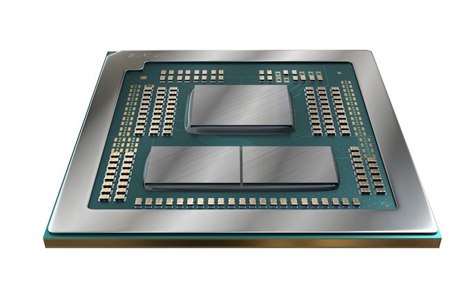
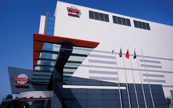
TSMC this week held its Arizona fab ‘first tool-in’ ceremony, where alongside celebrating its first US fab, the company also announced major expansion plans for the production facility. The world’s largest foundry is set to invest tens of billions of dollars in the next phase of its Fab 21 near Phoenix, Arizona, to significantly expand its capacity and start production of chips on its N3 process technologies there by 2026. (by which point N3 will be a trailing-edge node)


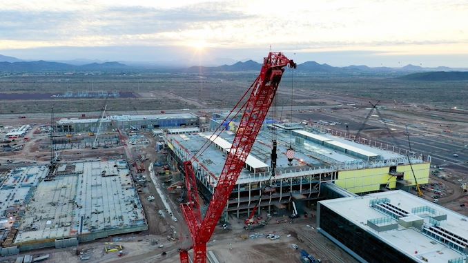
Construction of TSMC’s Fab 21 phase 1 in Arizona was completed earlier this year, and this week the company began installation of production tools into the facility. The fab will be equipped with tools from companies like ASML, Applied Materials, KLA, Lam Research, and Tokyo Electroni in the next few quarters, and it is scheduled to come online in early 2024. The fab will be producing chips using various process technologies that belong to TSMC’s N5 family, which now includes N5, N5P, N4, N4P, and N4X nodes. Production capacity of this phase of the fab will be around 30,000 wafer starts per month (WSPM), though the precise number will depend on actual technologies and designs.


Companies like AMD, Apple, and NVIDIA are set to run orders through Fab 21 phase 1 to produce their advanced chips in the U.S. for the first time in years. 


But that isn’t all that TSMC has in store for Fab 21. The company has announced that they now intend to build a second fab on the site, further expanding their US production capacity and setting up an even newer production line.


The new Arizona fab will expand TSMC’s capacity at the site to around 50,000 WSPM and will bring TSMC’s total investments in the site to $40 billion. Notably, that’s a $28B jump over the initial $12B investment TSMC made in their first Arizona fab, underscoring how costs continue to rise for newer fabs, but also that TSMC is becoming more comfortable with making larger infrastructure investments within the US. TSMC expects annual revenue from Arizona fabs to be in $10 billion per year ballpark, according to a Reuters report. Meanwhile, TSMC’s clients using the fabs will generate about $40 billion in revenue selling products made by the foundry in the U.S.


Set to come online in 2026, the second Arizona fab will be starting life a generation ahead of its initial counterpart, producing chips on TSMC’s N3 family of production nodes, which includes N3, N3E, N3P, N3S, and N3X. TSMC is expected to deliver its first N3 chips to a client in early 2023, so while the fab still represents cutting-edge technology as of the time of its inception, by the time it comes online it will technically be a trailing-edge fab. TSMC has previously indicated that they would be keeping leading-edge production within Taiwan – in large part because that’s where their actual R&D takes place – so the company’s updated Arizona fab plans are consistent with that stance.


With regards to capacity, the new Arizona fab, like its existing sibling, will be another MegaFab in TSMC parlance. That is to say a mid-range fab producing around 25,000 wafer starts per month. TSMC hasn’t disclosed a specific output figure for just the new fab, but with Fab 21 slated to offer 20,000 wafers per month, it looks like this fab will be a bit bigger, at closer to 30,000 wafers per month. Still, with a combined capacity of 50,000 wafers per month, TSMC’s Arizona facility is still among one of TSMC’s smaller operations – 50,000 wafers is only half the production capacity a single one of TSMC’s class-leading GigaFabs. So even with a second fab line, TSMC’s US operations will only represent a relatively small fraction of the company’s overall chip fab capacity.


Looking forward, TSMC has already begun construction of the second Arizona fab, and given the usual fab construction timelines, we can expect the shell to be complete by early 2024. After which it will take TSMC around another two years to equip it.


Meanwhile, TSMC is set to start producing chips using its N2 node in Taiwan in the second half of 2025. That node will use will be TSMC’s first node to use their nanosheet-based gate-all-around field-effect transistors (GAAFETs), and over time will gain backside power delivery. Still, since not all products need a leading-edge node, TSMC won’t have any trouble lining up customers for their N3 US domestic capacity.


“A strong, geographically diverse, and resilient supply chain is essential to the global semiconductor industry,” said Lisa Su, chief executive and chairman of AMD. “TSMC’s investment and expansion in Arizona is extremely important and mission critical for both the semiconductor industry and our extended ecosystem of partners and customers. AMD expects to be a significant user of the TSMC Arizona fabs and we look forward to building our highest performance chips in the United States.”


Source: TSMC


Source: AnandTech – TSMC Unveils Major U.S. Fab Expansion Plans: 3nm and Billion by 2026

Site News: December 1st Outage

As many of you noticed, AnandTech has spent several hours offline today. We are still in recovery mode at the moment (as I write this, the site has been restored to a copy from November 25th), but now that our major restoration efforts are completed, I wanted to offer you guys a brief update on the status of AnandTech.


At around 13:00 UTC (5am PT) today, the on-site cloud storage for AnandTech’s hosting provider became corrupted. As a result, AnandTech (and some other sites) were brought offline. Due to the nature of the corruption and the need to begin restoration efforts ASAP, we opted to restore the site from an off-site cold storage backup, rather than trusting the questionable on-site storage.


This is the first time we’ve ever had to execute our off-site data recovery plan before. And while it meant AT took a bit longer to restore than would be ideal, ultimately everything worked out and proved the necessity for off-site backups.


We’re still working to restore content from the last few days. Articles will be back, but we’ve likely lost any comments and user account registrations/updates made since midday Friday. Sorry about that! And thank you for bearing with us during today’s outage.


Source: AnandTech – Site News: December 1st Outage

Sponsoed Post: Trying to Pick Out Your New RTX 40 Series GPU? ASUS Has Two Mighty Options For You

ASUS is introducing two versions of the GeForce RTX 4090 and 4080 in its Republic of Gamers and TUF Gaming lines, giving gamers stylish and robust options for the latest graphics cards.


Source: AnandTech – Sponsoed Post: Trying to Pick Out Your New RTX 40 Series GPU? ASUS Has Two Mighty Options For You

WD_BLACK P40 Game Drive USB 3.2 Gen 2×2 Portable SSD Review: Balanced Storage

Western Digital had announced new products in the WD_BLACK lineup back in May 2022 to augment their offerings in the gaming market. The WD_BLACK P40 Game Drive SSD was part of the set, and became widely available last quarter. Western Digital has positioned the portable drive (PSSD) as a mid-range alternative to the premium WD_BLACK P50 Game Drive SSD. Sporting a USB 3.2 Gen 2×2 (20 Gbps) interface, the drive launched at a much lower price point compared to the P50 despite the addition of RGB lighting to the case. What corners has Western Digital cut in this mid-range offering, and what do gamers have to lose in going with the P40 over competing PSSDs? This review provides some answers.


Source: AnandTech – WD_BLACK P40 Game Drive USB 3.2 Gen 2×2 Portable SSD Review: Balanced Storage

Intel Launches Raptor Canyon: Desktop Raptor Lake Sizzles in NUC13 Extreme

Intel is officially taking the wraps off the first member of their Raptor Lake-based NUC13 family today. The NUC13 Extreme (like the three previous Extreme NUCs) caters to the gamers and content creators requiring leading edge performance and high-end discrete GPU support. Unlike the mainstream NUCs which have been consistently maintaining an ultra-compact form-factor profile, the Extreme family has slowly grown in size to accommodate flagship CPUs and discrete GPUs. These systems integrate a motherboard in a PCIe add-in card form factor (the Compute Element) and a baseboard that provides additional functionality with PCIe slots and other I/O features. As a refresher, Intel created the NUC Extreme category with the introduction of the Ghost Canyon NUC family in 2019. This was followed by the Tiger Lake-based Beast Canyon NUC in 2021 and the Alder Lake-based Dragon Canyon NUC earlier this year. The latest member of this family is today’s introduction – the Raptor Canyon NUC based on the Shrike Bay Compute Element.


The NUC Extreme family has grown in physical footprint with each generation, and the NUC13 Extreme is Intel’s biggest one yet. Coming in at 317mm x 129mm x 337mm (13.7L), this is more of a traditional tower desktop than the NUCs that the market has grown accustomed to. However, this size has allowed Intel to integrate flagship components. The Shrike Bay Compute Element supports socketed LGA 1700 processors with a PL1 of 150W and PL2 of 250W (tau of 28s). The vertical centering of the baseboard within the case enables plenty of isolation between the Compute Element on the top and the discrete GPU on the bottom. Triple-slot dGPUs up to 12.5″ in length are supported.


The NUC13 Extreme Kit comes in three flavors, while the Shrike Bay Compute Element itself has six variations. These allow system integrators and OEMs to offer a wide variety of systems targeting different market segments. The table below summarizes the key differences between the three NUC13 Extreme kits.


Intel NUC13 Extreme Kits (Raptor Canyon)
Model NUC13RNGi9 NUC13RNGi7 NUC13RNGi5
CPU Intel Core i9-13900K

Raptor Lake, 8P + 16E / 32T

5.8 GHz (Turbo) / 5.4 GHz (P) / 4.3 GHz (E)

125W TDP (Up to 253W)
Intel Core i7-13700K

Raptor Lake, 8P + 8E / 24T

5.4 GHz (Turbo) / 5.3 GHz (P) / 4.2 GHz (E)

125W TDP (Up to 253W)
Intel Core i5-13600K

Raptor Lake, 6P + 8E / 20T

5.1 GHz (Turbo) / 5.1 GHz (P) / 3.9 GHz (E)

125W TDP (Up to 181W)
GPU Intel UHD Graphics 770 (300 MHz – 1.65 GHz) Intel UHD Graphics 770 (300 MHz – 1.60 GHz) Intel UHD Graphics 770 (300 MHz – 1.50 GHz)
Memory 2x DDR5-5600 SODIMMs

(up to 64GB)
Motherboard (Compute Element) 295.3mm x 136.5mm x 46.1mm (Custom)
Storage 1x CPU-attached PCIe 4.0 x4 M.2 2280

1x PCH-attached PCIe 4.0 x4 M.2 2242 / 2280

1x PCH-attached PCIe 4.0 x4 / SATA M.2 2242 / 2280

2x SATA 6 Gbps (on baseboard)
I/O Ports 2x USB4 / Thunderbolt 4 (Type-C) (Rear)

6x USB 3.2 Gen 2 Type-A (Rear)

1x USB 3.2 Gen 2 Type-C (Front)

2x USB 3.2 Gen 1 Type-A (Front)
Networking Intel Killer Wi-Fi 6E AX1690i

(2×2 802.11ax Wi-Fi inc. 6 GHz + Bluetooth 5.2 module)

1× 2.5 GbE port (Intel I226-V)

1x 10 GbE port (Marvell AQtion AQC113C)
Display Outputs 2x DP 2.0 (1.4 certified) (via Thunderbolt 4 Type-C, iGPU)

1x HDMI 2.1 (up to 4Kp60) (rear, iGPU)
Audio / Codec 7.1 digital (over HDMI and Thunderbolt 4)

Realtek ALC1220 Analog Audio / Microphone / Speaker / Line-In 3.5mm (Rear)

USB Audio 3.5mm combo audio jack (Front)
Enclosure Metal

Kensington lock with base security
Power Supply FSP750-27SCB 750W Internal PSU
Dimensions 337mm x 317mm x 129mm / 13.7L
Chassis Expansion One PCIe 5.0 x16 with triple-slot GPU support up to 317.5mm in length
Customizable RGB LED illumination on chassis underside

CEC support for HDMI port

Power LED ring in front panel

3-year warranty


Each kit SKU corresponds to a NUC13SBB Shrike Bay Compute Element. In addition, Intel is also readying the NUC13SBBi(9/7/5)F variants that come with the KF processors – those Compute Elements do not have any Thunderbolt 4 ports. The HDMI port / graphics outputs are also not present. The three KF SKUs also forsake the 10GbE port.


The block diagram below gives some insights into the design of the system in relation to the I/O capabilities. Note that the system continues to use the Z690 chipset that was seen in the Dragon Canyon NUC.


PCIe x16 bifurcation (x8 + x8) is possible for the Gen 5 lanes. However, the baseboard design in the Raptor Canyon NUC kits does not support it. This is yet another aspect that OEMs could use to differentiate their Shrike Bay-based systems from the NUC13 Extreme.


Intel has provided us with a pre-production engineering sample of the flagship Raptor Canyon NUC (augmented with an ASUS TUF Gaming RTX 3080Ti GPU) for review, and it is currently being put through the paces. The 150W PL1 and microarchitectural advances in Raptor Lake have ensured that the benchmark scores are off the charts compared to the previous NUC Extreme models, albeit at the cost of significantly higher power consumption. On the industrial design side, I have been very impressed. By eschewing a fancy chassis and opting for a simple cuboid, Intel has ensured that all the I/O ports are easily accessible, installation of components is fairly straightforward, and cable management is hugely simplified. The increased dimensions of the chassis are well worth these advantages over the previous NUC Extreme models. Stay tuned for a comprehensive review later this week.


Source: AnandTech – Intel Launches Raptor Canyon: Desktop Raptor Lake Sizzles in NUC13 Extreme