Western Digital Unveils Dual Actuator Ultrastar DC HS760 20TB HDD

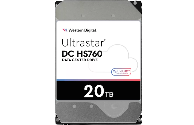
Without much fanfare, Western Digital this week introduced its first dual actuator hard drive, a 20TB drive that is designed to offer SATA SSD-like sequential read/write performance. The Ultrastar DC HS760 drive is meant to increase IOPS-per-terabyte performance for hyperscale cloud datacenters and will compete against Seagate’s dual actuator Exos 2X family of HDDs. Meanwhile, Western Digital’s offering will also mark the latest deployment of the company’s OptiNAND technology.


The dual actuator Ultrastar DC HS760 HDD builds upon the company’s single actuator Ultrastar DC HC560 drive which uses nine 2.2TB ePMR (energy-assisted perpendicular magnetic recording) platters. But in the case of the HS760, WD adds a second actuator to the drive, essentially splitting it up into two quasi-independent drives with each half having domain over 4.5 platters (9 surfaces). By doubling the number of indepent actuators, Western Digital claims that the HS760 is able to double sequential read/write speeds and increase random read/write performance by 1.7 times versus single actuator drives.


While the company yet has to upload a datasheet for its dual actuator HDD, we are looking at sequential throughput rates of around 582 MB/s, which interestingly enough is a tad faster than SATA SSDs, which max out the SATA-III at around 550 MB/s. Though it’s worth noting that, as is typical for enterprise-focused hard drives, Western Digital is using Serial Attached SCSI (SAS) here, so it won’t be possible to hook the drive up to a SATA host.


Since the two actuators inside Western Digital’s Ultrastar DC HS760 HDD work independently, the unit presents itself as two independent logical unit number (LUN) devices, and both logical hard drives are independently addressable. This means that datacenters will have to introduce certain software tweaks (i.e., these are not drop-in compatible with infrastructure designed for single actuator HDDs). But for the added complexity on the software/configuration side of matters, data center operators are being promised not only the aforementioned higher performance levels, but also a setup that is 37% more energy efficient in terms of IOPS-per-Watt than two 10TB devices.  In essence, hyperscalers are getting many of the benefits of having two current-generation 10TB HDDs, but in a product that takes up the space of just a single drive.


The key advantage of Western Digital’s Ultrastar DC HS760 20TB over hard drives with one actuator of the same capacity is significantly increased performance on an IOPS-per-TB basis. Typical enterprise-grade 3.5-inch HDDs with capacities between 8TB and 16TB offer random performance of 6 – 10 IOPS per terabyte, which is enough to ensure quality-of-service of datacenters. But at 20TB, random performance drops to less than 5 IOPS per terabyte, which requires hyperscalers to introduce various mitigations to ensure that these drives meet their QoS requirements.


Such mitigations either include implementing command queuing and latency-bounded I/O (LBIO) in firmware, usage of drives of lower capacity, reducing usable capacity per drive, or even adding sophisticated caching methods. All of these methods either increase upfront costs and/or total-costs-of-ownership. Therefore, hyperscalers need drives that can physically increase their IOPS-per-terabyte performance and dual actuator HDDs are a natural answer. As an added bonus, these hard drives also offer two times higher sequential read/write speeds than single-actuator HDDs.


As noted above, Western Digital is not the only company to offer dual actuator HDDs as Seagate has been doing this for years now. But Western Digital’s Ultrastar DC HS760 has an advantage over rivals that comes in the form of its OptiNAND technology, which is an integrated iNAND UFS embedded flash drive (EFD) coupled with firmware tweaks. OptiNAND is meant to increase capacity, reliability, and performance of HDDs and while Western Digital yet has to disclose performance numbers of its Ultrastar DC HS760 drives, it is at least evident that its 20TB drive will offer more capacity than Seagate’s competing Exos 2X18 18TB drive.


Otherwise, given that the HS760 is aimed primarily at hyperscalers, Western Digital is treating the drive as a product for a limited audience. Although the drive is listed on the company’s website, for example, there is no public pricing listed, and buyers will have to make a sales inquiry. So the actual unit pricing on the new drive is going to vary some, depending on things like order volumes and agreements between Western Digital and its clients.


Western Digital’s Ultrastar DC HS760 HDD will be covered with a five-year warranty with each LUN rated for a 500 TB annual workload.


Source: AnandTech – Western Digital Unveils Dual Actuator Ultrastar DC HS760 20TB HDD

Samsung Portable SSD T7 Shield 4TB Review: IP65 PSSD Gets a Capacity Upgrade

Samsung has been enjoying market success with their lineup of portable SSDs, starting with the T1 back in 2015. The company has been regularly updating their PSSD lineup with the evolution of different high-speed interfaces as well as NAND flash technology.


In early 2022, the company launched the Portable SSD T7 Shield, a follow-up to the Portable SSD T7 (Touch) introduced in early 2020. Introduced in models with capacities up to 2TB, the ruggedness / IP65 rating of the T7 Shield was advertised as a selling point over the regular Portable SSD T7 and T7 Touch. The company launched a 4TB version in this lineup in mid-January for the EU market. Samsung is officially bringing over the new capacity SKU to the North American market today. Read on for a comprehensive look at the performance and value proposition of the Portable SSD T7 Shield 4TB.


Source: AnandTech – Samsung Portable SSD T7 Shield 4TB Review: IP65 PSSD Gets a Capacity Upgrade

ASRock Industrial NUCS BOX-1360P/D4 Review: Raptor Lake-P Impresses, plus Surprise ECC

Low-power processors have traditionally been geared towards notebooks and other portable platforms. However, the continued popularity of ultra-compact form-factor desktop systems has resulted in UCFF PCs also serving as lead vehicles for the latest mobile processors. Such is the case with Intel’s Raptor Lake-P – the processor SKUs were announced earlier this month at the 2023 CES, and end-products using the processor were slated to appear in a few weeks. Intel is officially allowing its partners to start selling their products into the channel today, and also allowing third-party evaluation results of products based on Raptor Lake-P to be published.


ASRock Industrial announced their Raptor Lake-P-based NUC clones as soon as Intel made the parts public. With the new platform, the company decided to trifurcate their offerings – a slim version (sans 2.5″ drive support) with DDR4 SODIMM slots in the NUCS BOX-13x0P/D4, a regular height version with 2.5″ drive support in the NUC BOX-13x0P/D4, and a slightly tweaked version of the latter with DDR5 SODIMM slots in the NUC BOX-13x0P/D5. The NUCS BOX-1360P is the company’s flagship in the first category, and the relative maturity of DDR4-based platforms has allowed them to start pushing the product into the channel early.


ASRock Industrial sampled us with a NUCS BOX-1360P/D4 from their first production run. We expected a run of the mill upgrade with improvements in performance and power efficiency. In the course of the review process, we found that the system allowed control over a new / key Raptor Lake-P feature that Intel hadn’t even bothered to bring out during their CES announcement – in-band ECC. Read on for a comprehensive look at Raptor Lake-P’s feature set for desktop platforms with detailed performance and power efficiency analysis.


Source: AnandTech – ASRock Industrial NUCS BOX-1360P/D4 Review: Raptor Lake-P Impresses, plus Surprise ECC

Seagate Confirms 30TB+ HAMR HDDs in Q3, Envisions 50TB Drives in a Few Years

Seagate this week confirmed plans to launch the industry’s first 30+ TB hard drive that uses its heat assisted magnetic recording (HAMR) technology, as well as reaffirming its commitment to release HDDs with capacities of 50 TB and higher in a few years. But before this happens, the company will release 22 TB and 24 TB HDDs that will rely on perpendicular magnetic recording (PMR) and shingled magnetic recording (SMR) technologies, respectively.


One More Play for PMR and SMR


Various energy assisted magnetic recording methods, such as HAMR, will be used for next generations of hard drives for years to come. But while PMR is running out of steam, it is still evolving. Seagate has managed to increase areal density enabled by its PMR + TDMR platform by around 10%, enabling 2.2 TB 3.5-inch HDD platters and thus 22 TB hard drives featuring 10 of such disks. Furthermore, by using shingled recording, these drives can have their capacity stretched to 22 TB.


These 22 TB and 24 TB Seagate Exos drives will likely be drop-in compatible with existing cloud datacenter hardware as well as infrastructure, and should not require extensive validation and certification procedures, unlike brand-new HAMR HDDs. As a result, Seagate’s customers will be able to deploy such hard drives fairly quickly and increase storage density and storage capacity of their datacenters.


Seagate is now ramping up production of its 22 TB hard drives for datacenters, so expect the company to start their shipments shortly. Seagate is not disclosing when exactly it will officially launch its 22 TB and 24 TB parts, but we would expect them to arrive before the company introduces its HAMR-based HDDs; so think Q1 or Q2.


30+ TB HDDs Coming in Q3


In fact, Seagate has been shipping HAMR HDDs to select customers for evaluation as well as inside its own Lyve storage systems for a while, but those drives featured capacities akin to those of PMR/CMR HDDs and were not available in huge volumes. With Seagate’s 2nd generation HAMR platform, the company is going after higher volumes, but it took the company quite some time to get there. The first pre-qualification high-capacity HAMR-based HDDs are only just now getting ready to head out to customers for evaluation.


“We are meeting or exceeding all product development milestones and reliability metrics, and we will be shipping pre-qualification units to key cloud customers in the coming weeks,” said Dave Mosley, chief executive of Seagate. 


Meanwhile, commercial HAMR hard drives with capacities of 30TB or higher will ship in third quarter of this year, which is in-line with what Seagate promised last year.


“As a result of this progress, we now expect to launch our 30-plus terabyte platform in the June quarter, slightly ahead of schedule,” said Mosley. “The speed of the initial HAMR volume ramp will depend on a number of factors, including product yields and customer qualification timelines.”


Initially Seagate will only offer its HAMR technology for its highest-capacity offerings for hyperscale datacenters, whom need maximum storage density and are willing to pay premium for the drives and for supporting infrastructure. As yields of HAMR-supporting media and the appropriate read/write heads increase, the technology will be applied for drives with lower capacities in a bid to cut down their production costs (fewer disks and heads, lower the costs). This is not going to happen overnight though, as the company needs to increase yields of HAMR drive components and the HDDs themselves to a comfortable level.


“I think this year, [the volume of HAMR HDDs] will probably still be relatively low,” said the head of Seagate. “Then the faster we can get the yields and scrap and all the costs that we can control down on the heads and media, then the faster we’ll be accelerating. I think that will happen in calendar year 2024 and calendar year 2025 will just continue to accelerate. The highest capacity points will be addressed, but also these midrange capacity points.”


50+ TB HDDs Will Be Here in a Few Years


Seagate’s launch of its first mass market 30+ TB HAMR hard drives platform will mark a milestone for the company and the whole industry. But apparently the company has another breakthrough to share at this time. The firm said this week that it had created 5 TB platters for 3.5-inch hard drives, which presumably entails new media, new write heads, and new read heads. 


“It was nearly four years ago to the day that I first shared our lab results demonstrating 3 TB per disk capacities,” explained Mosley. “And today, we have demonstrated capacities of 5 TB per disk in our recording physics labs.”


For now, these platters are used on spinstands for evaluation and testing purposes, but platters like these will allow for 50 TB HDDs a few years down the line. Seagate’s roadmap indicates that such hard drives will hit the market sometimes in calendar 2026. 


It is unclear how thin the new platters are. But following current trends of nearline HDD evolution — increasing areal density and increasing number of platters per hard drive — it’s not outside the realm of possibility that Seagate will find ways to integrate even more than 10 platters in future drives. In which case Seagate would be able to hit drive sizes even larger than 50 TB.


In any case, with ~3 TB platters in production, samples of ~30 TB HDDs shipping to customers, and 5 TB platters demonstrated in the lab, Seagate’s HAMR roadmap seems to look quite solid. Therefore, expect hard drives to gain capacities rapidly in the coming years.


Source: AnandTech – Seagate Confirms 30TB+ HAMR HDDs in Q3, Envisions 50TB Drives in a Few Years

The Intel Core i9-13900KS Review: Taking Intel's Raptor Lake to 6 GHz

Back at Intel’s Innovation 2022 event in September, the company let it be known that it had plans to release a ‘6 GHz’ processor based on its Raptor Lake-S series of processors. Though it didn’t come with the same degree of fanfare that Intel’s more imminently launching 13900K/13700K/13600K received, it put enthusiasts and industry watchers on notice that Intel still had one more, even faster Raptor Lake desktop chip waiting in the wings.

Now a few months later, Raptor Lake’s shining moment has arrived. Intel has launched the Intel Core i9-13900KS, a 24-core (8x Perf + 16x Efficiency) part with turbo clock speeds of up to 6 GHz. A mark, which until very recently, was unprecedented without the use of exotic cooling methods such as liquid nitrogen (LN2). 

In what is likely to be one of the last in a wide range of Raptor Lake-S SKUs to be announced, Intel has seemingly saved its best for last. The Intel Core i9-13900KS is the faster and unequivocal bigger brother to the Core i9-13900K, with turbo clock speeds of up to 6 GHz while maintaining its halo presence with a 200 MHz increase on both P-core and E-core base frequencies.

Intel’s focus and strategy on delivering halo-level processors in limited supply is something that’s become a regular part of their product stack over the last few years. We’ve previously seen the Core i9-9900KS (Coffee Lake) and i9-12900KS (Alder Lake), which were relative successes in showcasing each Core architecture at their finest point. The Core i9-13900KS looks to follow this trend, although it comes as we’ve reached a time where power efficiency and costs are just a few widely shared concerns globally.

Having the best of the best is somewhat advantageous when there’s a need for cutting-edge desktop performance, but at what cost? Faster cores require more energy, and more energy generates more heat; 6 GHz for the average consumer is finally here, but is it worth taking the plunge? We aim to find out in our review of the 6 GHz Core i9-13900KS.


Source: AnandTech – The Intel Core i9-13900KS Review: Taking Intel’s Raptor Lake to 6 GHz

Intel Reports Q4 2022 and FY 2022 Earnings: 2022 Goes Out on a Low Note

Kicking off yet another earnings season, we once again start with Intel. The reigning 800lb gorilla of the chipmaking world is reporting its Q4 2022 and full-year 2022 financial results, closing the book on what has turned an increasingly difficult year for the company. As Intel’s primary client and datacenter markets have reached saturation on the back of record sales and spending is slowing for the time being, Intel is seeing significant drops in revenue for both markets. These headwinds, though not unexpected, have broken Intel’s 6-year streak of record yearly revenue – and sent the company back into the red for the most recent quarter.

Starting with quarterly results, for the fourth quarter of 2022, Intel reported $14.0B in revenue, which is a major, 32% decline versus the year-ago quarter. With Intel coming off of what was their best Q4 ever just a year ago, as the saying goes: the higher the highs, the lower the lows. As a result, Q4’22 will go down in the books as a money-losing quarter for Intel (on a GAAP basis), with the company losing $661M for the quarter, a 114% decline in net income. Overall, Intel’s revenue for the quarter was low end of their already conservative forecasted range.


Source: AnandTech – Intel Reports Q4 2022 and FY 2022 Earnings: 2022 Goes Out on a Low Note

Intel NUC 12 Pro Wall Street Canyon Kits Review: Alder Lake in UCFF Avatar

Intel introduced the ultra-compact form-factor in 2012 to reinvigorate the PC market. The incredible success of the product line has now resulted in the brand name propagating to other novel system configurations and form factors. The introduction of the mainstream Alder Lake NUCs last year – the NUC 12 Pro (Wall Street Canyon) – marked a decade-long journey for the original design. As part of bringing out the versatility of the form-factor and its evolution over the last ten years, Intel sampled three top-end Wall Street Canyon NUCs targeting different market segments – the NUC12WSKi7 for traditional business and consumer users, the NUC12WSKv7 in a slightly more eye-catching designer chassis for business and enterprise deployments, and the NUC12WSBi70Z in a rugged fanless case for IoT / Edge applications in industrial environments. Read on for a comprehensive analysis of the mainstream NUC 12 Pro mini-PC platform.


Source: AnandTech – Intel NUC 12 Pro Wall Street Canyon Kits Review: Alder Lake in UCFF Avatar

SK hynix Intros LPDDR5T Memory: Low Power RAM at up to 9.6Gbps

In a bit of a surprise move, SK hynix this week has announced a new variation of LPDDR5 memory technology, which they are calling LPDDR5T. Low Power Double Data Rate 5 Turbo (LPDDR5T) further ramps up the clockspeeds for LPDDR5-type memory, with SK hynix stating that their new memory will be able to clock at high as 9.6Gbps/pin, 13% faster than their top-bin 8.5Gbps LPDDR5X. According to the company, the memory is sampling now to partners as a 16GB part, with mass production set to begin in the second half of this year.


SK hynix is positioning LPDDR5T as an interim memory technology to cover the gap between LPDDR5X and the future development of LPDDR6, offering what amounts to a half-step up in memory bandwidth for customers who would like something faster than what contemporary LPDDR5X memory is capable of. That standard, as it currently stands, only goes to 8533Mbps, so any LPDDR5-type memory clocked higher than that is technically outside of the official JEDEC specification. Still, SK hynix’s announcement comes a bit unexpectedly, as while it’s not unusual for memory manufacturers to announce new technologies ahead of the industry’s standardization body, there hadn’t been any previous chatter of anyone coming to market with a further evolution of LPDDR5.


At this point the technical details on the new memory are limited. SK hynix was able to confirm that LPDDR5T will operate at the same voltages as LPDDR5X, with a VDD voltage range of 1.01v to 1.12v (nominally 1.05v) and a VDDQ of 0.5v. Coupled with that, as previously mentioned the new memory will max out at a data rate of 9.6Gbps/pin, which for a 64-bit part would mean a full data rate of 76.8GB/second. Otherwise, at this point all outward appearances are that LPDDR5T is just higher clocked LPDDR5X, given a new name since its data rate is outside the scope of LPDDR5X.


LPDDR Generations
  LPDDR4 LPDDR4X LPDDR5 LPDDR5X LPDDR5T

(Provisional)
Max Density 64 Gbit 32 Gbit 32 Gbit?
Max Data Rate 4266Mbps 6400Mbps 8533Mbps 9600Mbps
Channels 2 1 4?
Width x32 (2x x16) x16 x64
Banks

(Per Channel)
8 8-16 16?
Bank Grouping No Yes Yes?
Prefetch 16n 16n 16n?
Voltage 1.1v Variable

Nominal: 1.05v

Max: 1.1v
Variable

Nominal: 1.05v

Max: 1.12v
Vddq 1.1v 0.6v 0.5v


But whatever LPDDR5T is (or isn’t), SK hynix tells us that they intend to make a proper JEDEC standard of it. The company is already working with JEDEC on standardization of the memory technology, and while this doesn’t guarantee that other memory vendors will pick up the spec, it’s a sign that LPDDR5T isn’t going to be some niche memory technology that only ends up in a few products. This also means that the rest of the pertinent technical details should be published in the none too distant future.


In the meantime, for their initial LPDDR5T parts, SK hynix is going to be shipping a multi-die chip in a x64 configuration. According to the company’s PR office, they’re producing both 12Gb and 16Gb dies, so there’s a potential range of options for package densities, with the 16GB (128Gbit) package being the largest configuration. All of this RAM, in turn, is being built on the company’s 1anm process, which is their fourth-generation 10nm process using EUV, and paired with High-K metal gates (HKMG).


SK hynix’s decision to go with only a x64 package out of the gate is a notable one, since these higher density packages are typically limited to use in high-end smartphones and other high-performance devices (laptops, servers, etc), underscoring the intended market. For their part, SK hynix has stated that they expect the application of LPDDR5T to “expand beyond smartphones to artificial intelligence (AI), machine learning and augmented/virtual reality (AR/VR)”. LPDDR memory has been seeing increasing use in non-mobile products, so this doesn’t come as a surprise given the high-end nature of the technology. Server hardware vendors in particular come to mind as potential customers, since those products can easily absorb any increased power consumption from the higher memory clockspeeds.


Wrapping things up, SK hynix says that they expect to begin mass production of LPDDR5T in the second half of this year. So depending on just when in the year that production begins, and when their downstream customers implement the new RAM, it could begin showing up in products as easy as the end of this year.


Source: AnandTech – SK hynix Intros LPDDR5T Memory: Low Power RAM at up to 9.6Gbps

ASRock DeskMeet B660 Review: An Affordable NUC Extreme?

ASRock was one of the earliest vendors to cater to the small-form factor (SFF) PC market with a host of custom-sized motherboards based on notebook platforms. Despite missing the NUC bus for the most part, they have been quite committed to the 5×5 mini-STX form-factor introduced in 2015. ASRock’s DeskMini lineup is based on mSTX boards and has both Intel and AMD options for the end-user. While allowing for installation of socketed processors, the form-factor could not support a discrete GPU slot. Around 2018, Intel started making a push towards equipping some of their NUC models with user-replaceable discrete GPUs. In order to gain some market share in that segment, ASRock introduced their DeskMeet product line early last year with support for socketed processors and a PCIe x16 slot for installing add-in cards. Read on for a detailed analysis of the features, performance, and value proposition of the DeskMeet B660 – a 8L SFF PC based on the Intel B660 chipset, capable of accommodating Alder Lake or Raptor Lake CPUs.


Source: AnandTech – ASRock DeskMeet B660 Review: An Affordable NUC Extreme?

The FSP Hydro G Pro 1000W ATX 3.0 PSU Review: Solid and Affordable ATX 3.0

With the ATX 3.0 era now well underway, we’ve been taking a look at the first generation of ATX 3.0 power supplies to hit the market. Introducing the 16-pin 12VHPWR connector, which can supply up to 600 Watts of power to PCIe cards, ATX 3.0 marks the start of what will be a slow shift in the market. As high-end video cards continue to grow in power consumption, power supply manufacturers are working to catch up with these trends with a new generation of PSUs – not only updating power supplies to meet the peak energy demands of the latest cards, but also to better handle the large swings in power consumption that these cards incur.


For our second ATX 3.0 power supply, we’re looking at a unit from FSP Group, the Hydro G Pro ATX 3.0. Unlike some of the other ATX 3.0 PSUs we’ve looked at (and will be looking at), FSP has taken a slightly different approach with their first ATX 3.0 unit: rather than modifying its best platform or releasing a new top-tier platform, FSP went with an upgrade of its most popular platform, the original Hydro G Pro. As such, the new Hydro G Pro ATX 3.0 1000W PSU doesn’t have especially impressive specifications on paper, but it boasts good all-around performance for an affordable price tag ($199 MSRP). That makes FSP’s platform notable at a time when most ATX 3.0 come with an early adopter tax, with FSP clearly aiming to entice mainstream users who may not currently need an ATX 3.0 PSU but would like to own one in case of future upgrades.


Source: AnandTech – The FSP Hydro G Pro 1000W ATX 3.0 PSU Review: Solid and Affordable ATX 3.0

TSMC's 3nm Journey: Slow Ramp, Huge Investments, Big Future

Last week, TSMC issued their Q4 and full-year 2022 earnings reports for the company. Besides confirming that TSMC was closing out a very busy, very profitable year for the world’s top chip fab – booking almost $34 billion in net income for the year – the end-of-year report from the company has also given us a fresh update on the state of TSMC’s various fab projects.


The big news coming out of TSMC for Q4’22 is that TSMC has initiated high volume manufacturing of chips on its N3 (3nm-class) fabrication technology. The ramp of this node will be rather slow initially due to high design costs and the complexities of the first N3B implementation of the node, so the world’s largest foundry does not expect it to be a significant contributor to its revenue in 2023. Yet, the firm will invest tens of billions of dollars in expanding its N3-capable manufacturing capacity as eventually N3 is expected to become a popular long-lasting family of production nodes for TSMC.


Slow Ramp Initially


“Our N3 has successfully entered volume production in late fourth quarter last year as planned, with good yield,” said C. C. Wei, chief executive of TSMC. “We expect a smooth ramp in 2023 driven by both HPC and smartphone applications. As our customers’ demand for N3 exceeds our ability to supply, we expect the N3 to be fully utilized in 2023.”


Keeping in mind that TSMC’s capital expenditures in 2021 and 2022 were focused mostly on expanding its N5 (5nm-class) manufacturing capacities, it is not surprising that the company’s N3-capable capacity is modest. Meanwhile, TSMC does not expect N3 to account for any sizable share of its revenue before Q3.


In fact, the No. 1 foundry expects N3 nodes (which include both baseline N3 and relaxed N3E that is set to enter HVM in the second half of 2023) to account for maybe 4% – 6% of the company’s wafer revenue in 2023. And yet this would exceed the contribution of N5 in its first two quarters of HVM in 2020 (which was about $3.5 billion).


“We expect [sizable N3 revenue contribution] to start in third quarter 2023 and N3 will contribute mid-single-digit percentage of our total wafer revenue in 2023,” said Wei. “We expect the N3 revenue in 2023 to be higher than N5 revenue in its first year in 2020.”


Many analysts believe that the baseline N3 (also known as N3B) will be used by Apple either exclusively or almost exclusively, which is TSMC’s largest customer that is willing to adopt leading-edge nodes ahead of all other companies, despite high initial costs. If this assumption is correct and Apple is indeed the primary customer to use baseline N3, then it is noteworthy that TSMC mentions both smartphone and HPC (a vague term that TSMC uses to describe virtually all ASICs, CPUs, GPUs, SoCs, and FPGAs not aimed at automotive, communications, and smartphones) applications in conjunction with N3 in 2023. 


N3E Coming in the Second Half


One of the reasons why many companies are waiting for TSMC’s relaxed N3E technology (which is entering HVM in the second half of 2023, according to TSMC) is the higher performance and power improvements, as well as even more aggressive logic scaling. Another is that the process will offer lower costs, albeit at the cost of a lack of SRAM scaling compared to N5, according to analysts from China Renaissance.


“N3E, with six fewer EUV layers than the baseline N3, promises simpler process complexity, intrinsic cost and manufacturing cycle time, albeit with less density gain,” Szeho Ng, an analyst with China Renaissance, wrote in a note to clients this week. 


Advertised PPA Improvements of New Process Technologies

Data announced during conference calls, events, press briefings and press releases
  TSMC
N3

vs

N5
N3E

vs

N5
Power -25-30% -34%
Performance +10-15% +18%
Logic Area


Reduction* %


Logic Density*
0.58x


-42%


1.7x
0.625x


-37.5%


1.6x
SRAM Cell Size 0.0199µm² (-5% vs N5) 0.021µm² (same as N5)
Volume

Manufacturing
Late 2022 H2 2023


Ho says that TSMC’s original N3 features up to 25 EUV layers and can apply multi-patterning for some of them for additional density. By contract, N3E supports up to 19 EUV layers and only uses single-patterning EUV, which reduces complexity, but also means lower density.


“Clients’ interest in the optimized N3E (post the baseline N3B ramp-up, which is largely limited to Apple) is high, embracing compute-intensive applications in HPC (AMD, Intel), mobile (Qualcomm, Mediatek) and ASICs (Broadcom, Marvell),” wrote Ho.


It looks like N3E will indeed be TSMC’s main 3nm-class working horse before N3P, N3S, and N3X arrive later on.


Tens of Billions on N3


While TSMC’s 3nm-class nodes are going to earn the company a little more than $4 billion in 2023, the company will spend tens of billions of dollars expanding its fab capacity to produce chips on various N3 nodes. This year the company’s capital expenditures are guided to be between $32 billion – $36 billion. 70% of that sum will be used on advanced process technologies (N7 and below), which includes N3-capable capacity in Taiwan, as well as equipment for Fab 21 in Arizona (N4, N5 nodes). Meanwhile 20% will be used for fabs producing chips on specialty technologies (which essentially means a variety of 28nm-class processes), and 10% will be spent on things like advanced packaging and mask production.


Spending at least $22 billion on N3 and N5 capacity indicates that TSMC is confident on the demand for these nodes. And there is a good reason for that: the N3 family of process technologies is set to be TSMC’s last FinFET-based family of production nodes for complex high-performance chips. The company’s N2 (2nm-class) manufacturing process will rely on nanosheet-based gate-all-around field-effect transistors (GAAFETs). In fact, analyst Szeho Ng from China Renaissance believes that a significant share of this year’s CapEx set for advanced technologies will be spent on N3 capacity, setting the ground for roll-out of N3E, N3P, N3X, and N3S. Since N3-capable fabs can also produce chips on N5 processes, TSMC will be able to use this capacity where there will be significant demand for N5-based chips as well.


“TSMC guided 2023 CapEx at $32-36bn (2022: US$36.3bn), with its expansion focused on N3 in Fab 18 (Tainan),” the analyst wrote in a note to clients. 


Since TSMC’s N2 process technology will only ramp starting in 2026, N3 will indeed be a long lasting node for the company. Furthermore, since it will be the last FinFET-based node for advanced chips, it will be used for many years to come as not all applications will need GAAFETs.


Source: AnandTech – TSMC’s 3nm Journey: Slow Ramp, Huge Investments, Big Future

Intel Unveils Core i9-13900KS: Raptor Lake Spreads Its Wings to 6.0 GHz

Initially mentioned during their Innovation 2022 opening keynote by Intel CEO Pat Gelsinger, Intel has unveiled its highly anticipated 6 GHz out-of-the-box processor, the Core i9-13900KS. The Core i9-13900KS has 24-cores (8P+16E) within its hybrid architecture design of performance and efficiency cores, with the exact fundamental specifications of the Core i9-13900K, but with an impressive P-core turbo of up to 6 GHz.


Based on Intel’s Raptor Lake-S desktop series, Intel claims that the Core i9-13900KS is the first desktop processor to reach 6 GHz out of the box without overclocking. Available from today, the Core i9-13900KS has a slightly higher base TDP of 150 W (versus 125 on the 13900K), 36 MB of Intel’s L3 smart cache, and is pre-binned through a unique selection process to ensure the Core i9-13900KS’s special edition status for their highest level of frequency of 6 GHz in a desktop chip out of the box, without the need to overclock manually.


Source: AnandTech – Intel Unveils Core i9-13900KS: Raptor Lake Spreads Its Wings to 6.0 GHz

Micron Launches 9400 NVMe Series: U.3 SSDs for Data Center Workloads

Micron is taking the wraps off their latest data center SSD offering today. The 9400 NVMe Series builds upon Micron’s success with their third-generation 9300 series introduced back in Q2 2019. The 9300 series had adopted the U.2 form-factor with a PCIe 3.0 x4 interface, and utilized their 64L 3D TLC NAND. With a maximum capacity of 15.36 TB, the drive matched the highest-capacity HDDs on the storage amount front at that time (obviously with much higher performance numbers). In the past couple of years, the data center has moved towards PCIe 4.0 and U.3 in a bid to keep up with performance requirements and unify NVMe, SAS, and SATA support. Keeping these in mind, Micron is releasing the 9400 NVMe series of U.3 SSDs with a PCIe 4.0 x4 interface using their now-mature 176L 3D TLC NAND. Increased capacity per die is also now enabling Micron to present 2.5″ U.3 drives with capacities up to 30.72 TB, effectively doubling capacity per rack over the previous generation.


Similar to the 9300 NVMe series, the 9400 NVMe series is also optimized for data-intensive workloads and comes in two versions – the 9400 PRO and 9400 MAX. The Micron 9400 PRO is optimized for read-intensive workloads (1 DWPD), while the Micron 9400 MAX is meant for mixed use (3 DWPD). The maximum capacity points are 30.72 TB and 25.60 TB respectively. The specifications of the two drive families are summarized in the table below.


Micron 9400 NVMe Enterprise SSDs
  9400 PRO 9400 MAX
Form Factor U.3 2.5″ 15mm
Interface PCIe 4.0 NVMe 1.4
Capacities 7.68TB

15.36TB

30.72
6.4TB

12.8TB

25.6TB
NAND Micron 176L 3D TLC
Sequential Read 7000 MBps
Sequential Write 7000 MBps
Random Read (4 KB) 1.6M IOPS (7.68TB and 15.36TB)

1.5M IOPS (30.72TB)
1.6M IOPS (6.4TB and 12.8TB)

1.5M IOPS (25.6TB)
Random Write (4 KB) 300K IOPS 600K IOPS (6.4TB and 12.8TB)

550K IOPS (25.6TB)
Power Operating 14-21 W (7.68TB)

16-25W (15.36TB)

17-25W (30.72TB)
14-21 W (6.40TB)

16-24W (12.8TB)

17-25W (25.6TB)
Idle ? W ? W
Write Endurance 1 DWPD 3 DWPD
Warranty 5 years


The 9400 NVMe SSD series is already in volume production for AI / ML and other HPC workloads. The move to a faster interface, as well as higher-performance NAND enables a 77% improvement in random IOPS per watt over the previous generation. Micron is also claiming better all round performance across a variety of workloads compared to enterprise SSDs from competitors.


The Micron 9400 PRO goes against the Solidigm D7-5520, Samsung PM1733, and the Kioxia CM6-R. The Solidigm D7-5520 is handicapped by lower capacity points (due to its use of 144L TLC), resulting in lower performance against the 9400 PRO in all but the sequential reads numbers. The Samsung PM1733 also tops out at 15.36TB with performance numbers similar to that of the Solidigm model. The Kioxia CM6-R is the only other U.3 SSD with capacities up to 30.72TB. However, its performance numbers across all corners lags well behind the 9400 PRO’s.


The Micron 9400 MAX has competition from the Solidigm D7-P5620, Samsung PM1735, and the Kioxia CM6-V. Except for sequential reads, the Solidigm D7-P5620 lags the 9400 MAX in performance as well as capacity points. The PM1735 is only available in an HHHL AIC form-factor and uses PCIe 4.0 x8 interface. So, despite its 8 GBps sequential read performance, it can’t be deployed in a manner similar to that of the 9400 MAX. The Kioxia CM6-V tops out at 12.8TB and has lower performance numbers compared to the 9400 MAX.


Despite not being the first to launch 32TB-class SSDs into the data center market, Micron has ensured that their eventual offering provides top-tier performance across a variety of workloads compared to the competition. We hope to present some hands-on performance numbers for the SSD in the coming weeks.


Source: AnandTech – Micron Launches 9400 NVMe Series: U.3 SSDs for Data Center Workloads

The AMD Ryzen 9 7900, Ryzen 7 7700, and Ryzen 5 5 7600 Review: Zen 4 Efficiency at 65 Watts

In Q3 of last year, AMD released the first CPUs based on its highly anticipated Zen 4 architecture. Not only did their Ryzen 7000 parts raise the bar in terms of performance compared with the previous Ryzen 5000 series, but it also gave birth to AMD’s latest platform, AM5. Some of the most significant benefits of Zen 4 and the AM5 platform include support for PCIe 5.0, DDR5 memory, and access to the latest and greatest of what’s available in controller sets. 

While the competition at the higher end of the x86 processor market is a metaphorical firefight with heavy weaponry, AMD has struggled to offer users on tighter budgets anything to sink their teeth into. It’s clear Zen 4 is a powerful and highly efficient architecture, but with the added cost of DDR5, finding all of the components to fit under tighter budget constraints with AM5 isn’t as easy as it once was on AM4.

AMD has launched three new processors designed to offer users on a budget something to get their money’s worth, with performance that make them favorable for users looking for Zen 4 hardware but without the hefty financial outlay. The AMD Ryzen 9 7900, Ryzen 7 7700, and Ryzen 5 7600 processors all feature the Zen 4 microarchitecture and come with a TDP of just 65 W, which makes them viable for all kinds of users, such as enthusiasts looking for a more affordable entry-point onto the AM5 platform.

Of particular interest is AMD’s new budget offering for the Ryzen 7000 series: the Ryzen 5 7600, which offers six cores/twelve threads for entry-level builders looking to build a system with all of the features of AM5 and the Ryzen 7000 family, but at a much more affordable price point. We are looking at all three of AMD’s new Ryzen 7000 65 W TDP processors to see how they stack up against the competition, to see if AMD’s lower-powered, lower-priced non-X variants can offer anything in the way of value for consumers. We also aim to see if AMD’s 65 W TDP implementation can shine on TSMC’s 5 nm node process with performance per watt efficiency that AMD claims is the best on the market.


Source: AnandTech – The AMD Ryzen 9 7900, Ryzen 7 7700, and Ryzen 5 5 7600 Review: Zen 4 Efficiency at 65 Watts

CES 2023: QNAP Brings Hybrid Processors and E1.S SSD Support to the NAS Market

Over the last few years, the developments in the commercial off-the-shelf (COTS) network-attached storage (NAS) market have mostly been on the software front – bringing in more business-oriented value additions and better support for containers and virtual machines. We have had hardware updates in terms of processor choices and inclusion of M.2 SSD slots (primarily for SSD caching), but they have not been revolutionary changes.


At CES 2023, QNAP revealed plans for two different NAS units – the all-flash TBS-574X (based on the Intel Alder Lake-P platform), and the ML-focused TS-AI642 (based on the Rockchip RK3588 app processor). While QNAP only provided a teaser of the capabilities, there are a couple of points worth talking about to get an idea of where the COTS NAS market is headed towards in the near future.


Hybrid Processors


Network-Attached storage units have typically been based on either server platforms in the SMB / SME space or single-board computer (SBC) platforms in the home consumer / SOHO space. Traditionally, both platforms have eschewed big.LITTLE / hybrid processors for a variety of reasons. In the x86 space, we saw hybrid processors entering the mainstream market recently with Intel’s Alder Lake family. In the ARM world, big.LITTLE has been around for a relatively longer time. However, server workloads are typically unsuitable for that type of architecture. Without a credible use-case for such processors, it is also unlikely that servers will go that route. However, SBCs are a different case, and we have seen a number of application processors adopting the big.LITTLE strategy getting used in that market segment.


Both the all-flash TBS-574X and the AI NAS TS-AI642 are based on hybrid processors. The TBS-574X uses the Intel Core i3-1220P (Alder Lake-P) in a 2P + 8E configuration. The TS-AI642 is based on the Rockchip RK3588 [ PDF ], with 4x Cortex-A76 and 4x Cortex-A55 fabricated in Samsung’s 8LPP process.


QNAP is no stranger to marketing Atom-based NAS units with 2.5 GbE support – their recent Jasper Lake-based tower NAS line-up has proved extremely popular for SOHO / SMB use-cases. The Gracemont cores in the Core i3-1220P are going to be a step-up in performance, and the addition of two performance cores can easily help with user experience related to features more amenable for use in their Core-based units.


NAS units have become powerful enough to move above and beyond their basic file serving / backup target functionality. The QTS applications curated by QNAP help in providing well-integrated value additions. Some of the most popular ones enable container support as well as the ability to run virtual machines. As the range of workloads run on the NAS simultaneously start to vary, hybrid processors can pitch in to improve performance while maintaining power efficiency.


On the AI NAS front, the Rockchip RK3588 has processor cores powerful enough for a multi-bay NAS. However, QNAP is putting more focus on the neural network accelerator blocks (the SoC has 6 TOPS of NN inference performance), allowing the NAS to be marketed to heavy users of their surveillance and ‘AI’ apps such as QVR Face (for face recognition in surveillance videos), QVR Smart Search (for event searching in surveillance videos), and QuMagie (for easily indexed photo albums with ‘AI’ functionality).


E1.S Hot-Swappable SSDs


QNAP’s first NASbook – an all-flash NAS using M.2 SSDs – was introduced into the market last year. The TBS-464 remains a unique product in the market, but goes against the NAS concept of hot-swappable drives.


QNAP’s First-Generation NASbook – the TBS-464


At the time of its introduction, there was no industry standard for hot-swappable NVMe flash drives suitable for the NASbook’s form-factor. U.2 and U.3 drive slots with hot-swapping capabilities did exist in rackmount units meant for enterprises and datacenters. So, QNAP’s NASbook was launched without hot-swapping support. Meanwhile, the industry was consolidating towards E1.S and E1.L as standard form-factors for hot-swappable NVMe storage.


(L to R) E1.S 5.9mm (courtesy of SMART Modular Systems); E1.S Symmetric Enclosure (courtesy of Intel); E1.S (courtesy of KIOXIA)


QNAP’s 2023 NASbook – the TBS-574X – will be the first QNAP NAS to support E1.S hot-swappable SSDs (up to 15mm in thickness). In order to increase drive compatibility, QNAP will also be bundling M.2 adapters attached to each drive bay. This will allow end-users to use M.2 SSDs in the NASbook while market availability of E1.S SSDs expands.


Specifications Summary


The TBS-574X uses the Intel Core i3-1220P (2P + 8E – 10C/12T) and includes 16GB of DDR4 RAM. Memory expansion support is not clear as yet (It is likely that these are DDR4 SO-DIMMs). There are five drive bays, and the NAS seems to be running QTS based on QNAP’s model naming). The NASbook also sports 2.5 GbE and 10 GbE ports, two USB4 ports (likely Thunderbolt 4 sans certification, as QNAP claims 40 Gbps support, and ADL-P supports it natively), and 4K HDMI output. The NASbook also supports video transcoding with the integrated GPU in the Core i3-1220P. QNAP is primarily targeting collaborative video editing use-cases with the TBS-574X.


The TS-AI642 uses the RockChip RK3588 (4x CA-76 + 4x CA-55) app processor. The RAM specifications were not provided – SoC specs indicate LPDDR4, but we have reached out to QNAP for the exact amount . There are six drive bays. This is again interesting, since the SoC natively offers only up to 3 SATA ports. So, QNAP is either using a port multiplier or a separate SATA controller connected to the PCIe lanes for this purpose. The SoC’s native network support is restricted to dual GbE ports, but QNAP is including 2.5 GbE as well as a PCIe Gen 3 slot for 10 GbE expansion. These are also bound to take up the limited number of PCIe lanes in the processor (which is 4x PCIe 3.0, configurable as 1 x4, or 2 x2, or 4 x1). Overall, the hardware is quite interesting in terms of how QNAP will be able to manage performance expectations with the SoC’s capabilities. With a focus on surveillance deployments and cloud storage integration, the performance may be good enough even with port multipliers.


Concluding Remarks


Overall, QNAP’s teaser of their two upcoming desktop NAS products has provided us with insights into where the NAS market for SOHOs / SMBs is headed in the near future. QNAP has never shied away from exploring new hardware options, unlike Synology, QSAN, Terramaster, and the like. While we are very bullish on E1.S support and hybrid processors in desktop NAS units, the appeal of the RockChip-based AI NAS may depend heavily on its price to capabilities / performance aspect.


Source: AnandTech – CES 2023: QNAP Brings Hybrid Processors and E1.S SSD Support to the NAS Market

A Lighter Touch: Exploring CPU Power Scaling On Core i9-13900K and Ryzen 9 7950X

One of the biggest running gags on social media and Reddit is how hot and power hungry CPUs have become over the years. Whereas at one time flagship x86 CPUs didn’t even require a heatsink, they can now saturate whole radiators. Thankfully, it’s not quite to the levels of a nuclear reactor, as the memes go – but as the kids say these days, it’s also not a nothingburger. Designing for higher TDPs and greater power consumption has allowed chipmakers to keep pushing the envelope in terms of performance – something that’s no easy feat in a post-Dennard world – but it’s certainly created some new headaches regarding power consumption and heat in the process. Something that, for better or worse, the latest flagship chips from both AMD and Intel exemplify.


But despite these general trends, this doesn’t mean that a high performance desktop CPU also needs to be a power hog. In our review of AMD’s Ryzen 9 7950X, our testing showed that even capped at a these days pedestrian 65 Watts, the 7950X could deliver a significant amount of performance at less than half its normal power consumption.


If you’ll pardon the pun, power efficiency has become a hot talking point these days, as enthusiasts look to save on their energy bills (especially in Europe) while still enjoying fast CPU performance, looking for other ways to take advantage of the full silicon capabilities of AMD’s Raphael and Intel’s Raptor Lake-S platforms besides stuffing the chips with as many joules as possible. All the while, the small form factor market remains a steadfast outpost for high efficiency chips, where cooler chips are critical for building smaller and more compact systems that can forego the need for large cooling systems.


All of this is to say that while it’s great to see the envelope pushed in terms of peak performance, the typical focus on how an unlocked chip scales when overclocking (pushing CPU frequency and CPU VCore voltages) is just one way to look at overall CPU performance. So today we are going to go the other way, and to take a look at overall energy efficiency for users – to see what happens when we aim for the sweet spot on the voltage/frequency curve. To that end, today we’re investigating how the Intel Core i9-13900K and AMD Ryzen 9 7950X perform at different power levels, and to see what kind of benefits power scaling can provide compared to stock settings.


Source: AnandTech – A Lighter Touch: Exploring CPU Power Scaling On Core i9-13900K and Ryzen 9 7950X

CES 2023: Akasa Introduces Fanless Cases for Wall Street Canyon NUCs

Akasa is one of the very few vendors to carry a portfolio of passively-cooled chassis solutions for the Intel NUCs. We had reviewed their Turing solution with the Bean Cayon NUC and the Newton TN with the Tiger Canyon NUC, and come away impressed with the performance of both cases. At CES 2023, the company is upgrading their portfolio of fanless NUC cases to support the mainstream NUC Pro using the 12th-Gen Core processors – the Wall Street Canyon.


Turing WS


The Turing WS builds upon the original Turing chassis to accommodate the updated I/Os of the Wall Street Canyon NUC.


The 2.7L chassis can be oriented either horizontally or vertically, and retains the ability to install a 2.5″ SATA drive. Improvements over the previous generations include the inclusion of an updated thermal solution for the M.2 SSD.


The Turing WS retains all the I/Os of the regular Wall Street Canyon kits and also includes antenna holes for those requiring Wi-Fi connection in the system. The company does offer suggested complementary additions to the build for that purpose – a tri-band Wi-Fi antenna and corresponding pigtails. We would like to see these getting included by default for the DIY versions of the Turing WS that get sold in retail.


Newton WS


The Newton WS is a minor update to the Newton TN that we reviewed last year.


The key change is the removal of the serial cable and corresponding rear I/O cut-out. In fact, Akasa indicates that the Newton TN can also be used with the Wall Street Canyon for consumers requiring the serial I/O support.


The 1.9L volume, additional USB ports in the front I/O (that are not available in the regular Wall Street Canyon kits), and VESA mounting support are all retained in the Newton WS.


Plato WS


The Plato WS is a slim chassis (39mm in height) that builds upon user feedback for the previous Plato cases. The key update over the Plato TN is the integration of support for the front panel audio jack.


The Plato WS carries over all the other attractive aspects of the product family – VESA and rack mounting support, 2.5″ drive installation support, serial port in the rear I/O, and additional USB 2.0 ports in the front panel.


In addition to the above three SKUs, Akasa also recently launched the Pascal TN, a passively-cooled IP65-rated case for the Tiger Canyon and Wall Street Canyon NUCs, making it suitable for outdoor installations.


Akasa’s main competition comes from fanless system vendors like OnLogic and Cirrus7 who prefer to sell pre-built systems with higher margins. In the DIY space, we have offerings like the HDPLEX H1 V3 and HDPLEX H1 TODD which unfortunately do not have wide distribution channels like Akasa’s products – as a result of lower volumes, the pricing is also a bit on the higher end. For Wall Street Canyon, Tranquil is also offering a DIY case in addition to their usual pre-built offerings. It remains to be seen whether the company remains committed to the DIY space.


Passively-cooled cases usually have a significant price premium that regular consumers usually don’t want to pay. Vendors like Akasa are bringing about a change in this category by offering reasonably-priced, yet compelling products via e-tailers. Simultaneous focus on industrial deployments and OEM contracts as well as consumer retail has proved successful for Akasa, as evidenced by their continued commitment to thermal solutions for different NUC generations.


Source: Akasa, FanlessTech


Source: AnandTech – CES 2023: Akasa Introduces Fanless Cases for Wall Street Canyon NUCs

CES 2023: IOGEAR Introduces USB-C Docking Solutions and Matrix KVM

IOGEAR has been servicing the computer accessories market with docks and KVMs for more than a couple of decades now. In addition to the generic use-cases, the company creates products that target niche segments with feature sets that are not available in products from other vendors. At CES 2023, IOGEAR is taking the wraps off a number of USB-C docks slated to get introduced over the next couple of quarters.


Docking Solutions


The three new products in this category fall under two categories – the first two utilize Display Link chips along with traditional USB-C Alt Mode support, while the third one uses the Intel Goshen Ridge Thunderbolt controller for 8K support in addition to the usual array of ports found in regular Thunderbolt 4 / USB4 docks. The following table summarizes the essential aspects of the three new products.


IOGEAR USB-C Docking Solutions @ CES 2023 (Dock Pro Series)
  Universal Dual View Docking Station Duo USB-C Docking Station USB4 8K Triple View
Model Name GUD3C4K2TAA GUD3CDHTAA GUD4C8K3
Upstream Port USB 3.2 Gen 2 Type-C 2x USB 3.2 Gen 2 Type-C (Dual Host Support) USB4 Type-C (40 Gbps)
Audio 1x 3.5mm Combo Audio Jack 1x Mic In

1x Speaker Out
1x 3.5mm Combo Audio Jack
USB-A 2x USB 3.2 Gen 1

1x USB 3.2 Gen 1 (12W charging)
2x USB 2.0

2x USB 3.2 Gen 2
2x USB 3.2 Gen 2

1x USB 3.2 Gen 1
USB-C 1x USB 3.2 Gen 2 1x USB 3.2 Gen 2 1x USB 3.2 Gen 2

2x USB4 (40Gbps with DP Alt Mode up to 8Kp30) downstream
Networking 1x GbE RJ-45 1x GbE RJ-45 1x 2.5 GbE RJ-45
Card Reader 1x SDXC UHS-II

1x microSDXC UHS-II
Display Outputs 2x HDMI 2.0a

2x Display Port 1.2a

(All via DisplayLink Chipset)

(Max. of 2x 4Kp60 Outputs)
2x Display Port 1.2a (4Kp60) (via DisplayLink Chipset)

1x HDMI 1.4a (4Kp30) (via DP Alt Mode)
2x HDMI 2.1 (up to 8Kp30)

2x Display Port 2.1 (up to 8Kp30)

(All via DP Alt Mode)
Host Power Delivery USB PD 3.0 (up to 100W) Up to 100W per host (total 200W) USB PD 3.0 (up to 96W)
Power Supply External 150W @ 20V/7.5A External 230W External 150W @ 20V/7.5A
Dimensions 91mm x 70mm x 17mm 219mm x 88mm x 32mm 225mm x 85mm x 18mm
Launch Date March 2023 June 2023 March 2023
MSRP $250 $300 $300


The Dock Pro Universal Dual View Docking Station is a premium DisplayLink-based dock capable of driving up to two 4Kp60 displays, with a choice of HDMI or DisplayPort for each.


The dock also includes host power delivery support, and the distribution of ports is presented above.


The Dock Pro Duo USB-C Docking Station is ostensibly a USB-C dock, but it incorporates features typically found in KVMs. It allows two systems to be simultaneously connected to the dock, and a push button in front to cycle between one of four display modes as show in the picture below.


The push button configures one of the two hosts to the DisplayLink chain (that is behind the two DisplayPort outputs). All the peripheral ports are seen by the host connected to that chain. At the same time, the HDMI port is kept active using the Alt Mode display output from the other host. Hot keys are available to cycle through the display modes to enable easy multi-tasking. This is an innovative combination of docking and KVM that I haven’t seen from other vendors yet.


Finally, we have the flagship USB4 / Thunderbolt 4 dock – the Dock Pro USB4 8K Triple View. It incorporates all the bells and whistles one might want from a TB4 dock, including downstream USB4 ports and 8K support.


Surprisingly, the pricing is quite reasonable at $300 – possibly kept that way by avoiding Thunderbolt certification. This product could appeal to a different audience compared to the Plugable TBT4-UDZ despite similar pricing, thanks to the availability of downstream ports. However, the product is slated to ship only towards the end of the quarter.


KVM Solutions


IOGEAR is also announcing the GCMS1922 2-port 4K Dual View DisplayPort Matrix KVMP with USB 3.0 Hub and Audio. Such KVMs with 4Kp60 support have typically been priced upwards of $500. This is no exception with a $530 MSRP. However, for this pricing, IOGEAR is incorporating a number of interesting features. The KVM can operate in either matrix or extension mode, with one computer driving both display outputs in the latter, and each host driving one display in the former. In the matrix mode, the KVM also supports crossover switching via movement of the mouse pointer (in addition to the regular physical button on the KVM and hotkeys). Audio mixing support (i.e, keeping the audio output of a ‘disconnected’ host also active) is available too, allowing the monitoring of notifications from both computers without having to switch sources.


The KVM provides two USB 3.2 Gen 1 and two USB 2.0 Type-A ports for downstream peripherals in addition to separate audio jacks for the speaker and microphone. It must be noted that the display outputs are HDMI, while the inputs are DisplayPort. The KVM switch is slated to become available later this quarter.


In addition to these upcoming products, IOGEAR is also demonstrating the KeyMander Nexus Gaming KVM and the MECHLITE NANO compact USB / wireless keyboard at the show. These products were introduced into the market last year.


Source: AnandTech – CES 2023: IOGEAR Introduces USB-C Docking Solutions and Matrix KVM

CES 2023: AMD Instinct MI300 Data Center APU Silicon In Hand – 146B Transistors, Shipping H2’23

Alongside AMD’s widely expected client product announcements this evening for desktop CPUs, mobile CPUs, and mobile GPUs, AMD’s CEO Dr. Lisa Su also had a surprise up her sleeve for the large crowd gathered for her prime CES keynote: a sneak peak at MI300, AMD’s next-generation data center APU that is currently under development. With silicon literally in hand, the quick teaser laid out the basic specifications of the part, along with reiterating AMD’s intentions of taking leadership in the HPC market.


First unveiled by AMD during their 2022 Financial Analyst Day back in June of 2022, MI300 is AMD’s first shot at building a true data center/HPC-class APU, combining the best of AMD’s CPU and GPU technologies. As was laid out at the time, MI300 would be a disaggregated design, using multiple chiplets built on TSMC’s 5nm process, and using 3D die stacking to place them over a base die, all of which in turn will be paired with on-package HBM memory to maximize AMD’s available memory bandwidth.


AMD for its part is no stranger to combining the abilities of its CPUs and GPUs – one only needs to look at their laptop CPUs/APUs – but to date they’ve never done so on a large scale. AMD’s current best-in-class HPC hardware is to combine the discrete AMD Instinct MI250X (a GPU-only product) with AMD’s EPYC CPUs, which is exactly what’s been done for the Frontier supercomputer and other HPC projects. MI300, in turn, is the next step in the process, bringing the two processor types together on to a single package, and not just wiring them up in an MCM fashion, but going the full chiplet route with TSV stacked dies to enable extremely high bandwidth connections between the various parts.


The key point of tonight’s reveal was to show off the MI300 silicon, which has reached initial production and is now in AMD’s labs for bring-up. AMD had previously promised a 2023 launch for the MI300, and having the silicon back from the fabs and assembled is a strong sign that AMD is on track to make that delivery date.


Along with a chance to see the titanic chip in person (or at least, over a video stream), the brief teaser from Dr. Su also offered a few new tantalizing details about the hardware. At 146 billion transistors, MI300 is the biggest and most complex chip AMD has ever built – and easily so. Though we can only compare it to current chip designs, this is significantly more transistors than either Intel’s 100B transistor Xeon Max GPU (Ponte Vecchio), or NVIDIA’s 80B transistor GH100 GPU. Though in fairness to both, AMD is stuffing both a GPU and a CPU into this part.


The CPU side of the MI300 has been confirmed to use 24 of AMD’s Zen 4 CPU cores, finally giving us a basic idea of what to expect with regards to CPU throughput. Meanwhile the GPU side is (still) using an undisclosed number of CDNA 3 architecture CUs. All of this, in turn, is paired with 128GB of HBM3 memory.


According to AMD, MI300 is comprised of 9 5nm chiplets, sitting on top of 4 6nm chiplets. The 5nm chiplets are undoubtedly the compute logic chipets – i.e. the CPU and GPU chiplets – though a precise breakdown of what’s what is not available. A reasonable guess at this point would be 3 CPU chiplets (8 Zen 4 cores each) paired with possibly 6 GPU chiplets; though there’s still some cache chiplets unaccounted for. Meanwhile, taking AMD’s “on top of” statement literally, the 6nm chiplets would then be the base dies all of this sits on top of. Based on AMD’s renders, it looks like there’s 8 HBM3 memory stacks in play, which implies around 5TB/second of memory bandwidth, if not more.


With regards to performance expectations, AMD isn’t saying anything new at this time. Previous claims were for a >5x improvement in AI performance-per-watt versus the MI250X, and an overall >8x improvement in AI training performance, and this is still what AMD is claiming as of CES.


The key advantage of AMD’s design, besides the operational simplicity of putting CPU cores and GPU cores on the same design, is that it will allow both processor types to share a high-speed, low-latency unified memory space. This would make it fast and easy to pass data between the CPU and GPU cores, letting each handle the aspects of computing that they do best. As well, it would significantly simplify HPC programming at a socket level by giving both processor types direct access to the same memory pool – not just a unified virtual memory space with copies to hide the physical differences, but a truly shared and physically unified memory space.


AMD FAD 2022 Slide


When it launches in the later half of 2023, AMD’s MI300 is expected to be going up against a few competing products. The most notable of which is likely NVIDIA’s Grace Hopper superchip, which combines an NVIDIA Armv9 Grace CPU with a Hopper GPU. NVIDIA has not gone for quite the same level of integration as AMD is, which arguably makes MI300 a more ambitious project, though NVIDIA’s decision to maintain a split memory pool is not without merit (e.g. capacity). Meanwhile, AMD’[s schedule would have them coming in well ahead of arch rival Intel’s Falcon Shores XPU, which isn’t due until 2024.


Expect to hear a great deal more from AMD about Instinct MI300 in the coming months, as the company will be eager to show off their most ambitious processor to date.


Source: AnandTech – CES 2023: AMD Instinct MI300 Data Center APU Silicon In Hand – 146B Transistors, Shipping H2’23

AMD Announces Ryzen 9 7900, Ryzen 7 7700, and Ryzen 5 7600 Processors: Zen 4 at 65 W

During its keynote at CES 2023, Dr. Lisa Su, AMD’s CEO, announced three new desktop processors based on its Zen 4 microarchitecture, the Ryzen 9 7900, Ryzen 7 7700, and Ryzen 5 7600. Each of these new processors includes a base TDP of 65 W with a reduction of all-core base frequency compared to the X-series SKUs. Designed to be a more affordable and cost-effective option for its latest AM5 platform, the new 65 W-based Ryzen 7000 SKUs come bundled with one of AMD’s Wraith coolers, with prices starting at $229 for the Ryzen 5 7600.


With the ever-pressing desire for high-performance levels in the desktop space, but with even higher levels of performance per watt, AMD’s unleashed three new derivatives of its existing Ryzen 7000 desktop CPUs. Still, with a base TDP of just 65 W, there is more to the story than bare TDP figures. AMD also uses Package Power Tracking (PPT) as a metric which typically sits higher; this is effectively the power levels given from the AM5 socket itself, coupled with Precision Boost Overdrive (PBO), which can yield increased levels of performance for at the cost of heat and power.


Source: AnandTech – AMD Announces Ryzen 9 7900, Ryzen 7 7700, and Ryzen 5 7600 Processors: Zen 4 at 65 W