Samsung and AMD Renew GPU Architecture Licensing Agreement: More RDNA Exynos Chips to Come

In a joint press release released this evening, AMD and Samsung have announced that the two companies are renewing their GPU architecture licensing agreement for Samsung’s Exynos SoCs. The latest multi-year deal between AMD and Samsung will see Samsung continuing to license AMD’s Radeon graphics architectures for use in the company’s Arm-based Exynos SoCs, with the two companies committing to work together over “multiple generations” of GPU IP.

The extension of the licensing agreement comes just shy of 4 years after Samsung and AMD announced their initial licensing agreement in June of 2019. The then-groundbreaking agreement would see Samsung license Radeon GPU IP for use in their flagship Exynos SoCs in an effort to get a jump on the mobile SoC market, tapping AMD’s superior Radeon graphics IP to get access to newer features and more efficient designs sooner than Samsung otherwise might have with their own internal efforts.


Source: AnandTech – Samsung and AMD Renew GPU Architecture Licensing Agreement: More RDNA Exynos Chips to Come

Asus Preps ROG Ally: A Portable Windows Game Console with Custom Zen 4 + RDNA 3 APU

Asus has begun teasing its own portable game console, the ROG Ally, which the company is positioning as a high-end offering for the handheld PC gaming market. With its ROG Ally, Asus is certainly trying to join in on the rise of portable x86-based game consoles, which have been inspired by the Steam Deck system and further stimulated by game developers’ enthusiasm to optimize their titles for these portable low-power PCs.


This weeks reveal, which included a questionably timed April Fool’s joke that was, in, fact, not a joke, is less of an announcement and more of a teaser on what Asus is working on. As such, Asus hasn’t revealed much in the way of detailed specifications, let alone a release date or pricing. None the less, the company feels confident enough in the product at this point that they’re showing off a prototype to whet gamers appetites ahead of what’s presumably a proper release later this year.


Source: AnandTech – Asus Preps ROG Ally: A Portable Windows Game Console with Custom Zen 4 + RDNA 3 APU

AMD Computing & Graphics EVP Rick Bergman to Retire – Jack Huynh Named Replacement

In a brief press release sent out yesterday afternoon, AMD has announced that its executive leadership team is going to see some changes. Rick Bergman, the current executive vice president of AMD’s important Computing and Graphics business group, has announced that he will be taking up retirement later in the quarter. In his place, long-time AMD executive and design engineer Jack Huynh has been appointed as the new senior vice president and general manager for the group.


Rick Bergman is a well-known name at AMD with a significant history at the company, most notably on the GPU side of the business. Prior to re-joining AMD in 2019 to lead the Compute and Graphics business unit, he was CEO of Synaptics from 2011 through 2019. Before leaving AMD the first time, Bergman worked at AMD (and earlier acquisition ATI) for over a decade, serving in various roles overseeing AMD’s GPU and CPU technologies, and helping to orchestrate AMD’s late 2000s graphics renaissance. This will mark the second (and final) time that Bergman is leaving the company, as he is retiring from AMD – though AMD notes that he will be sticking around through the current quarter “to ensure a smooth transition.”


In his place, long-time AMD executive (and design engineer) Jack Huynh has been tapped to lead the Computing and Graphics group. Huynh has been at AMD for over two decades, and prior to his new appointment, he was the senior vice president and general manager for AMD’s rather successful Semi-Custom business group for several years. With his new position, Huynh will have broad dominion over AMD’s desktop chip efforts, covering both CPUs and GPUs, including the ongoing development of AMD’s next generation of consumer and gaming products.


“Under Jack’s leadership, AMD has strengthened our position as the leading provider of custom solutions for gaming,” said Dr. Su. “We see strong long-term growth opportunities for our Computing and Graphics business as we bring our high-performance CPU and GPU IP together with our leadership software capabilities to create differentiated solutions across our foundational gaming franchise and a broader set of markets. As we welcome Jack in his expanded role, I also want to personally thank Rick for his many contributions and dedication to our business throughout his years with AMD.”


Source: AnandTech – AMD Computing & Graphics EVP Rick Bergman to Retire – Jack Huynh Named Replacement

The AMD Ryzen 7 7800X3D Review: A Simpler Slice of V-Cache For Gaming

In February, AMD released the first parts in its highly anticipated Ryzen 7000X3D series. This new line combines AMD’s 3D V-Cache packaging with high-performance and highly efficient Zen 4 cores. Two out of the three X3D series processors were available for the initial launch, including the flagship Ryzen 9 7950X3D and the slightly lower-spec Ryzen 9 7900X3D. However, AMD may have saved the best for last. Today, we will be looking at the third sibling from the Ryzen 7000X3D line-up, the long-awaited Ryzen 7 7800X3D.


The AMD Ryzen 7 7800X3D is the direct successor to last year’s highly successful Ryzen 7 5800X3D, boasting 8 Zen 4 CPU cores, a base core frequency of 4.2 GHz, and a boost clock of up to 5.0 GHz. But what sets this processor apart from its predecessor is that it’s using AMD’s latest Zen 4 cores, built on TSMC’s 5 nm node, which promises to take power and performance efficiency to the next level for gamers. Perhaps the biggest advantage of the Ryzen 7 7800X3D is its massive 96 MB of L3 cache, thanks to AMD’s implementation of its 3D V-Cache packaging technology in cooperation with TSMC. Our reviews of the previous generation Ryzen 7 5800X3D and the behemoth Ryzen 9 7950X3D have shown this technology to be a success – sometimes, massively so – in specific games that are able benefit from the additional L3 cache.


Overall, the Ryzen 7 7800X3D appears to be a promising addition to the Ryzen 7000X3D lineup. Its impressive 96 MB of L3 cache and coming with the added benefits of Zen 4 cores make it a strong contender for gamers. However, it remains to be seen how it will perform in real-world applications compared to other current generation chips on test, as well as looking at how the performance in gaming stacks up.


Source: AnandTech – The AMD Ryzen 7 7800X3D Review: A Simpler Slice of V-Cache For Gaming

Microsoft Launches Thunderbolt 4 Surface Dock – Sans Surface Connect Port

Microsoft has introduced a new docking station for its latest Surface devices equipped with Thunderbolt 4 ports. The Surface Thunderbolt 4 Dock has eight ports and provides a comprehensive collection of eight current USB Type-C and legacy USB Type-A connectors along with a 2.5GbE. One of the main selling points of the dock is support for enterprise-grade features. But, perhaps most notably, the dock does not have a Surface Connect port.


Microsoft’s Surface Thunderbolt 4 Dock connects to a compatible host featuring USB4/Thunderbolt 4 and comes with three 10 Gbps USB 3.1 Gen 2 Type-A connectors and three 40 Gbps Thunderbolt 4/USB4-certified USB Type-C ports that are accompanied by 2.5GbE and a TRRS audio connector for headsets. The docking station can support two 4Kp60 monitors and various bandwidth hungry TB3/TB4/USB4 peripherals such as storage and eGFX external GPU boxes.


Also, the unit has an internal power supply that can feed its host up to 96W of power, which is enough to power a high-end 15 or 16-inch laptop. Yet, it cannot feed more than 15W of power over its USB-C ports, so its charging capabilities are pretty limited.


Microsoft stresses that its Surface Thunderbolt 4 Dock is different from its previous docks as it can be used with non-Surface USB-C devices, including Windows OEM devices and Apple Macs. As part of this compatibility, the dock lacks the company’s proprietary Surface Connect port, which has been a mainstay of Microsoft Surface devices up until now – for better and for worse. Dropping the proprietary port makes it incompatible with older Surface devices that only have a Surface Connect port, such as the Microsoft Surface Book 2 and the Surface Pro 5, but looking at the bigger picture, Microsoft’s release of a dock that lacks its own proprietary port may indicate that the company is (finally) dropping it entirely in favor of the more ubiquitous Thunderbolt 4/USB4 connector.


With its six ports, an audio connector, and a 2.5GbE port, the Microsoft Surface Thunderbolt 4 Dock somewhat falls short from being an ultimate docking station (such as 13-in-1 and 14-in-1 docks from OWC). Yet, it looks like its key selling point is not exactly the number of connectors, but rather support for enterprise-grade features, making it a comprehensive choice for commercial customers buying Microsoft Surface or other Windows-based devices.


In particular, the Surface Thunderbolt 4 Dock offers Firmware Update via Windows Update, Wake on LAN from Modern Standby, and MAC Address Pass-Through‎. Additionally, the Surface Enterprise Management Mode (SEMM) allows for easy disabling of the dock ports in mission-critical environments and limits functionality to specific devices‎ (e.g., one can plug in a monitor, a keyboard or a webcam, but cannot use a USB drive).


Microsoft’s Surface Thunderbolt 4 Dock will be available shortly directly from Microsoft as well as from its resellers for $299.


Source: AnandTech – Microsoft Launches Thunderbolt 4 Surface Dock – Sans Surface Connect Port

AMD Quietly Launches A620 Platform: Sub $100 AM5 Motherboards

AMD rather unexpectedly introduced its entry-level A620 platform for AM5 processors late last week. The new platform is designed to power inexpensive PCs that use AMD’s CPUs in AM5 packaging based on the Zen 4 microarchitecture and to cut down costs; it omits support for overclocking, PCIe Gen5 connectivity of any kind, and USB 3.2 Gen2x2. Most importantly, base AMD A620-based motherboards will not support higher-wattage CPUs.


Disabling some connectivity is meant to simplify testing and validation procedures and the design of actual motherboards. On the platform hardware side of matters, the AMD A620 chipset uses the same Promontory 21 silicon as the more expensive B650 and X670 chipsets, but in this case, AMD cut down some of the features supported by silicon. In particular, A620 does not support 10Gbps USB 3.2 Gen2x2, only supports eight PCIe 3.0 lanes (depending on the exact motherboard configuration, the number of enabled lanes may vary), only supports two 10Gbps USB 3.2 Gen2 ports and two 5Gbps USB 3.0 ports.


Regarding motherboard design, AMD also does not mandate its partners to support processors with a TDP higher than 65W, so in many cases (if not most of them) cases A620-based mainboards will not support any Ryzen 7000X or Ryzen 7000X3D CPUs. Our colleagues from Tom’s Hardware note that AMD does not explicitly prohibit motherboards makers from supporting high-wattage gaming processors on A620-powered motherboards, but since the platform is meant to be cheap, we can only guess whether there will be many A620 mainboards that feature a sophisticated voltage regulating module for higher-end CPUs. 


On the bright side, A620-based motherboards support factory-overclocked memory with EXPO profiles up to DDR5-6000; it is uncertain whether further manual memory tuning is permitted.


Also, A620 platforms do not support CPU-enabled PCIe Gen5 x4 and x16 interconnections and only feature PCIe Gen4 speeds, which lowers production costs. Yet, they will support four 10Gbps USB 3.2 Gen2 ports enabled by the CPU.


Given the absence of client GPUs supporting a PCIe 5.0 x16 interface, which is unlikely to change for at least a year, and the minimal advantages of PCIe 5.0 x4 SSDs over those with a PCIe 4.0 x4 interface for DirectStorage-enabled games, it seems that opting for PCIe 4.0 speeds instead of PCIe 5.0 for cheap platforms is reasonably practical.


Speaking of cheap AMD AM5 platforms in general, it should be noted that AMD only has three AM5 processors with a 65W TDP, including 12-core Ryzen 9 7900, eight-core Ryzen 7 7700, and six-core Ryzen 5 7600. The latter currently costs $229, which is not particularly cheap. Furthermore, this one has a very low-end integrated GPU, so it will need a discrete graphics card, which is not cheap these days either.


As for prices of actual A620 motherboards, only ASRock currently offers two of such platforms in the U.S. One costs $86, and another is priced at $100 over at Newegg. Meanwhile, it remains to be seen how cheap or expensive similar A620-based platforms from such makers as Asus, Biostar, Gigabyte, and MSI will be.


Over time AMD will, of course, release inexpensive AM5 APUs with proper built-in graphics, and this is when its A620 platform will undoubtedly come in handy. But for now, AMD’s Ryzen 7000-series processors mainly target gamers, and the latter are more likely to opt for a Ryzen 7000X chip with enhanced performance and overclocking support or a Ryzen 7000X3D processor with expanded cache for superior single-thread performance, which is going to benefit from more advanced B650-powered motherboards. That said, we can only guess how popular will AMD A620 platform will be before AMD rolls out cheaper AM5 processors.


Source: AnandTech – AMD Quietly Launches A620 Platform: Sub 0 AM5 Motherboards

Kioxia and Western Digital Debut 218-Layer 3D NAND: 1Tb TLC with 3.2 GT/s IO Speed

Kioxia and Western Digital formally introduced their 8th Generation BiCS 3D NAND memory with 218 active layers. The new storage device offers a 1Tb capacity in 3D TLC mode and features 3200 MT/s data transfer speed, a combination that will enable SSD makers to build high-performance, high-capacity drives. To enable such an extreme interface speed, the companies adopted an architecture akin to YMTC’s Xtacking.


The 218-layer BiCS 3D NAND device jointly developed by Kioxia and Western Digital supports triple-level cell (TLC) and quad-level cell (QLC) configurations to maximize storage density and expand addressable applications. The companies said that the new device embraces their new ‘lateral shrink technology to increase bit density by over 50’ without elaborating. Considering that the flash memory IC increased the number of active layers by 34%, the claim about a 50% bit density increase indicates that developers also shrank lateral sizes of NAND cells to fit in more of them per layer. 


Meanwhile, the 218-layer 3D NAND device features a quad-plane architecture allowing for a higher level of parallelism for programming and read times and increased performance. In addition, the 218-layer 3D TLC device also has a 3200 MT/s (which could provide a 400 MB/s peak read/write speed) input/output interface, which is the highest I/O speed announced so far. High data transfer rates will be handy for high-end client and enterprise SSDs featuring a PCIe 5.0 interface.


Kioxia and Western Digital Fab 7, Yokkaichi Plant, Japan


The key innovation of the 8th Generation BiCS 3D NAND memory is the all-new CBA (CMOS directly Bonded to Array) architecture that implicates separate production of 3D NAND cell array wafers and I/O CMOS wafers using the most optimal process technologies and then bonding them together to create a final product that offers increased bit density and fast NAND I/O speed. Meanwhile, Kioxia and Western Digital must disclose details about their CBA architecture and whether the I/O CMOS wafers carry other NAND peripheral circuitry, like page buffers, sense amplifiers, and charge pumps.


Producing memory cells and peripheral circuits separately solves several problems as it allows manufacturers to make them using the most efficient process technologies in their sections of cleanrooms. This brings further benefits as the industry adopts methods like string stacking. 


Kioxia said it had started sample shipments of 8th Generation BiCS 3D NAND memory devices to select customers. Still, there is no word when the company expects to initiate volume production of its next-generation flash memory. It is not unusual for companies to announce new types of 3D NAND quarters before they enter mass production, so it is reasonable to expect 8th Gen BICS on the market in 2024.


Through our unique engineering partnership, we have successfully launched the eighth-generation BiCS Flash with the industry’s highest 1-bit density,” said Masaki Momodomi, Chief Technology Officer at Kioxia Corporation. “I am pleased that Kioxia’s sample shipments for limited customers have started. By applying CBA technology and scaling innovations, we’ve advanced our portfolio of 3D flash memory technologies for use in various data-centric applications, including smartphones, IoT devices, and data centers.


Source: AnandTech – Kioxia and Western Digital Debut 218-Layer 3D NAND: 1Tb TLC with 3.2 GT/s IO Speed

Synopsys Intros AI-Powered EDA Suite to Accelerate Chip Design and Cut Costs

Synopsys has introduced the industry’s first full-stack AI-powered suite of electronic design automation tools that covers all stages of chip design, from architecture to design and implementation to manufacturing. The Synopsys.ai suite promises to radically reduce development time, lower costs, improve yields, and enhance performance. The set of tools is set to be extremely useful for chips set to be made on leading-edge nodes, such as 5nm, 3nm, 2nm-class, and beyond.


Chip Design Challenges


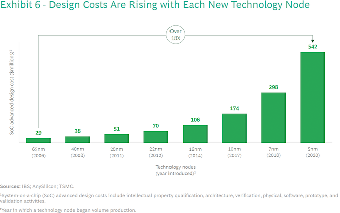
As chips gain complexity and adopt newer process technologies, their design and manufacturing costs escalate to unprecedented levels. Designing a reasonably complex 7 nm chip costs about $300 million (including ~ 40% for software). In contrast, the design cost of an advanced 5 nm processor exceeds $540 million (including software), according to International Business Strategies (IBS) estimates. At 3 nm, a complex GPU will cost about $1.5 billion to develop, including circa 40% for software. 


The traditional ‘waterfall’ semiconductor design approach is perhaps one of the reasons why chip development costs skyrocket so rapidly. It takes hundreds (if not thousands) of engineers and thousands of servers over several years to develop and simulate architectural, structural, logic, and layout designs. Meanwhile, every design stage involves tasks that are essential for the quality of the chip, but they are iterative and time-consuming in nature. For obvious reasons, as chips get more complex, each design change gets longer as companies cannot throw in as many engineers as they want to a given task because the number of people they have is limited.


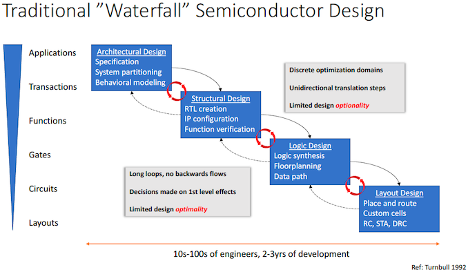
Things get more challenging as the waterfall approach almost excludes backward flows, so people implementing one of the thousands of possible place and route designs have little to zero influence on the architectural or structural design. As a result, the only way to avoid inefficiencies resulting in higher-than-expected costs, lower-than-expected performance, and/or higher-than-expected power consumption is to make different design teams work closer together at all stages. Yet, this gets harder as design cycles get longer.


Manufacturing costs at 5 nm and 3 nm production nodes are also noticeably higher than those on previous-generation fabrication technologies. The latest leading-edge manufacturing processes extensively use extreme ultraviolet lithography and more expensive raw materials (e.g., pellicles for photomasks, resists, etc.). Therefore, it gets even more crucial for chip developers to build close-to-perfect designs that are cheaper to make.


In general, the semiconductor industry faces several challenges these days as it needs to cut down development time, maintain (or even reduce) chip development costs, and ensure predictable manufacturing costs. Everything has to be done when the industry faces a deficit of highly skilled engineers. 


This is where the Synopsys.ai EDA suite comes into play. 


From Scratch to High-Volume Manufacturing


The Synopsys.ai full-stack EDA suite consists of three key applications the DSO.ai AI for chip design: the Synopsys VSO.ai for functional verification, and the TSO.ai for silicon test. The suite is designed to speed up iterative and time-consuming chip design stages using machine learning and reinforcement learning accelerated by modern CPUs and GPUs. 


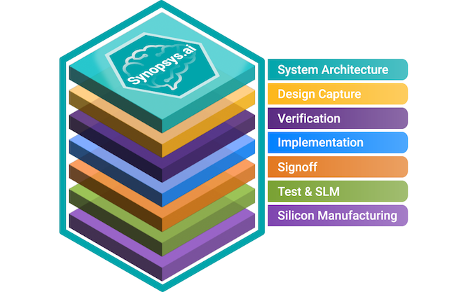
Synopsys has been offering its DSO.ai place and route AI-driven solution for about two years now, and over 100 designs have been taped out using the EDA tool so far. But this time around, the company is looking at fast-tracking all design stages with AI. The software suite can be used at all stages, including simulations, design capture, IP verification, physical implementation, signoff, test, and manufacturing. 


Better Architectures Delivered Faster


Small groups of very talented engineers typically develop microarchitectures, and this stage is considered by many as an intersection of technology and art. In fact, microarchitectures are developed fairly quickly too. Synopsys says that even this stage can be accelerated and improved with AI as artificial as, unlike people, machines can quickly estimate the most efficient architecture parameters and data paths. 


The General Manager of Synopsys’s Electronic Design Automation Group (EDA), Shankar Krishnamoorthy, states, “The whole process of developing a chip starts with the architecture of the chip and there are a lot of decisions to be made there,”  He also went on to say “How big does your cache need to be? What kind of interfaces run between your computer and memory? What configurations of memory should you consider, so there are many, many choices there, which an architecture expert would explore rapidly, and then converge on what are the right parameters to implement the chip with. So that process itself is something where AI can be used to rapidly explore that solution space […] and produce an even better result that they may not have gotten to, just because of the compute power that AI can work with.


Another aspect of using AI for microarchitectural explorations is boosting the microarchitecture development capabilities of a given company amid shortages of experienced architects. 


Shankar Krishnamoorthy also said, “In cases when you have an expert architect already there, AI is really an assistant. The modern AI techniques are really good at zooming in on the spaces of interest in a very large parameter space by using rewards and penalties. Then you [end up with] a set of menu of choices (such as tradeoffs between power and performance) from which the architect sort of picks the best one for the workload of interest.


Speeding Up IP Verification


Functional and IP verification is a chip design step that takes up a lot of time. It is imperative to test each IP individually and ensure that it functions correctly before integrating them, as the complexity of verification increases exponentially when multiple IPs are combined. Meanwhile, it is crucial to achieving a high level of test coverage for each individual IP. 


Nowadays, the common approach for verifying IP involves the designer creating a test benchmark that reflects their verification strategy. This test benchmark is then simulated using conventional simulation techniques, such as constrained random simulation, with the help of a traditional simulator. Achieving high target coverage for a given IP faster is a challenge that can be addressed by the Synopsys VSO.ai, which is part of Synapsys.ai.


By embedding techniques like reinforcement learning deep into the simulation engine, you can achieve that target coverage” said the head of Synopsys’s EDA group. “You say, I need 99% coverage of this IP, you can achieve that target coverage in a much shorter period of time, and using much fewer simulations, because essentially, that reinforcement learning engine that is embedded into the simulation engine is constantly [communication] with the engine that is generating the stimulus.” 


Renesas confirmed that the Synapsys VSO.ai software could both expand target coverage and speed up the IP verification process.


Takahiro Ikenobe, who is the IP Development Director of the Shared R&D Core IP Division at Renesas, said, “Meeting quality and time-to-market constraints is fast becoming difficult using traditional human-in-the-loop techniques due to the ramp in design complexity. Using AI-driven verification with Synopsys VSO.ai, part of Synopsys.ai, we have achieved up to 10x improvement in reducing functional coverage holes and up to 30% increase in IP verification productivity demonstrating the ability of AI to help us address the challenges of our increasingly complex designs.


Place and Route Done Fast


Speaking of increasingly complex designs, we must remember how hard it is to realize the modern processor’s design physically. While modern EDA tools streamline chip development, skilled human engineers are still required to efficiently implement chip floorplan, layout, placement, and routing, utilizing their experience to create efficient designs. Although experienced engineers typically work fast, they are limited in their ability to evaluate hundreds of design options, explore all potential combinations, and simulate tens or even hundreds of different layouts to identify the optimal design within a reasonable timeframe. As a result, in many cases, they implement their best-known methodologies, which may not be the most efficient ones for a particular chip made on a particular production node.


This is when they can use the Synopsys DSO.ai platform that does not need to simulate all the possible ways to place and route a chip but leverages artificial intelligence to evaluate all combinations of architectural choices, power and performance targets, geometries and then simulate a few different layouts to find the one that complies with desired performance, power, area, and cost (PPA) combination in a fraction of the time. 


Speaking of simulation, it is important to note that simulating a physically large chip (whether a CPU, GPU or a memory IC) is rather hard to accomplish. Traditionally chip designers used large machines based on CPUs or FPGAs to simulate future chips. Still, recently Synopsys applied GPU acceleration for these workloads and got a several-fold performance uplift.


If we look at the design of discrete memory, like DRAM or NAND flash, these are very large circuits that need to be simulated for electrical correctness, physical correctness, you know, stress, IR drop all the other types of effects,” Krishnamoorthy told us. “Simulation of these very large discrete memory structures is very time-consuming. That’s an area where we have successfully applied GPU acceleration in order to achieve several-fold acceleration of the time it takes to simulate these large circuits.”


One of the interesting things that Synopsys mentioned during our conversation is that the DSO.ai tool can be used to implement analog circuits — which barely (if at all) scale with each new node — in accordance with new design rules. 


Fundamentally, if you take a PLL, or you take any other type of analog circuit, and you are really not changing the circuit itself, you are migrating it from, let’s say, 7 nm to 5 nm or 5 nm to 3 nm,” explained the Synopsys executive. “That process of migrating a circuit from one node to another is something that is ripe for automation and ripe for the application of AI. So that is another area where we have applied AI to accelerate that process and cut down the effort and time needed to migrate analog circuits by a significant amount.


According to Synopsys, comparable AI capabilities can simplify the task of transferring chip designs between diverse foundries or process nodes. However, it is worth considering that intricate designs’ power, performance, and area characteristics (PPAc) are customized for specific nodes. It remains uncertain whether AI can effectively migrate such a design from one foundry to another while preserving all the key characteristics and whether potential trade-offs of such a migration could be significant.


Synopsys has been offering its DSO.ai platform for about a couple of years, and by now, about 170 chip designs implemented using this EDA tool have been taped out.


We talked about crossing the 100 tape out milestone in January,” said Krishnamoorthy. “We are close to 170 now, so the pace of adoption of that AI-based physical design is really fast among the customer base.


Test and Silicon Lifecycle Management


After a chip was implemented and produced, chip designers need to verify that everything works fine in a process that is somewhat similar to IP verification. This time around, no simulations are involved. Instead, a chip is inserted into a tester device, and specific test patterns are run to confirm that the chip is operating correctly. Therefore, the number of patterns required to test an SoC or an actual system is a major concern for product engineering departments. 


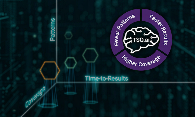
The Synopsys TSO.ai tool is designed to help semiconductor companies generate the right test patterns, cut the number of patterns they have to run by 20% to 30% and speed up the silicon test/verification phase. The same test sequences are then used to test all mass-produced chips to ensure they function correctly. The duration of the testing phase directly impacts costs, so it is particularly crucial, especially for high-volume parts.


We have shown how AI can cut down the total number of patterns needed in order to test circuits by a significant amount,” said the Synopsys executive. “We are talking about 20% to 30% type of reductions in test patterns. So that directly translates to cost of test and time on the tester, which is a big deal for companies.


Make Chip Designs Cheaper


Using AI-enabled tools in chip development can speed up their time to market and reduce their development and production costs significantly. Depending on the exact design, Synopsys says we are looking at, at least a 30% – 40% range, and now that hardware development costs of complex chips reach $325 million (at 5 nm) – $900 million (at 3 nm), we are talking about a lot of money.


Chip costs are obviously hard to estimate,” said Shankar Krishnamoorthy. “If I had to guess, I would say, [cost reduction from AI tools usage is] definitely in the 30% to 40% range.


Normally, engineering costs account for around 60% of a chip design cost, whereas compute costs account for approximately 40%. AI can be used to reduce both kinds of costs, according to Synopsys.


When an established company designs a new chip, it comprises 30% to 40% of new IP and 60% to 70% of seasoned IP, said Krishnamoorthy. Traditionally, many engineers migrate IPs from the previous node to the next node, often porting over 60% to 70% of the IPs with minor modifications. However, this is an inefficient use of resources. Instead, by leveraging AI to apply previous learnings to the next generation, the time and resources required to complete these incremental blocks can be dramatically reduced, allowing human engineers to expedite the process.


When it comes to new IP blocks, determining the best way to architect and implement them can be challenging and uncertain, often requiring at least one engineer per block. This approach can impact the number of people needed for the project to converge. However, leveraging AI as an assistant can rapidly explore and learn about new designs and architectures to determine the optimal strategy for implementation, verification, and testing. This can significantly reduce the investment needed for new blocks.


Finally, deploying DSO.ai, VSO.ai, and TSO.ai more widely can reduce the compute cost by enabling more intelligent runs of EDA tools. Rather than relying on a trial-and-error approach and indiscriminately simulating all kinds of circuits, targeted AI-enabled runs can be used to achieve similar results. In the end, compute costs will decrease.


Summary


Synopsys.ai is the industry’s first suite of EDA tools that can address all phases of chip design, including IP verification, RTL synthesis, floor planning, place and route, and final functional verification. 


The usage of machine learning and reinforcement learning enabled for time-consuming and iterative designed stages such as design space exploration, verification coverage, regression analytics, and test program generation, promises to reduce design costs, lower production costs, increase yields, boost performance, and reduce time-to-market. The set of tools can be particularly useful for chips set to be made on leading-edge nodes, such as 5nm, 3nm, 2nm-class, and beyond.


Furthermore, offloading some of the duties to AI-enabled EDA tools can significantly decrease the load on engineering teams, freeing up their time and minds to develop new features, enhance product differentiation, or design more chips, according to Synopsys.


The company says that top chip designers already use its Synopsys.ai, though not all chips are designed with AI assistance for now.


One of the interesting things that Synopsys pointed out is that its Synapsys.ai software suite mostly relies on CPU acceleration for AI. While select things like large circuit simulations can be accelerated using GPUs, most of the workloads run on Intel CPUs.


Source: AnandTech – Synopsys Intros AI-Powered EDA Suite to Accelerate Chip Design and Cut Costs

The XPG Fusion Titanium 1600 PSU Review: Outrageous Power, Outstanding Quality

One of the perks of normality largely returning to the PC components market now that the crypto mining bubble has popped has been a return to normal with regards to component availability. Video cards were of course the biggest change there – even if prices on the latest generation remain higher than many would like to see – but crypto farms were also soaking up everything from CPUs and RAM to power supplies. So after a period of almost two years of high-powered PSUs of all flavors being hard to come by, the PSU market is also returning to normal.


The collapse of crypto mining and underlying improvement of electronics components has also meant that high-power PSU designs have reverted, in a sense. PSU vendors are finally making some fresh investments in high-end, high-efficiency designs – PSUs that crypto miners would have never paid the premium for. Especially with the launch of the new ATX 3.0 standard and its 12VHPWR connection, there’s an opportunity for a new generation of PSUs to make their mark while powering the latest video cards.


There are few power supplies where this is more apparent than XPG’s new Fusion Titanium 1600. The sole member of its class, the Fusion is a true flagship-grade PSU with the electronics quality to match. Built by Delta Electronics, the XPG Fusion makes liberal use of Gallium Nitride MOSFETs in order to deliver a monstrous 1600 Watts of power at 80 Plus Titanium levels of efficiency. All the while this will also be one of the first high powered ATX 3.0 power supplies, offering two 12VHPWR connectors – making it suitable to drive two high-end video cards – which is no small feat given the power excursion requirements that come with the ATX 3.0 specification.


To that end, today we are thoroughly exploring everything that makes the XPG Fusion stand out from the crowd. From its oversized chassis to its almost absurd voltage regulation quality, it’s a power supply that few customers will ever need, but certainly makes its mark across the PSU design ecosystem.


Source: AnandTech – The XPG Fusion Titanium 1600 PSU Review: Outrageous Power, Outstanding Quality

Intel Updates Data Center Roadmap: Xeons On Track – Emerald in Q4'23, Sierra Forest in H1'24

Coming to the end of the first quarter of 2023, Intel’s Data Center and AI group is finding itself at an interesting inflection point – for reasons both good and bad. After repeated delays, Intel is finally shipping their Sapphire Rapids CPUs in high volumes this quarter as part of the 4th Generation Xeon Scalable lineup, all the while its successors are coming up very quickly. On the other hand, the GPU side of the business has hit a rough spot, with the unexpected cancellation of Rialto Bridge – what would have been Intel’s next Data Center GPU Max product. It hasn’t all been good news in the past few months for Intel’s beleaguered data center group, but it’s not all bad news, either.


It’s been just over a year since Intel last delivered a wholesale update on its DCAI product roadmaps, which were last refreshed at their 2022 investors meeting. So, given the sheer importance of the high margin group, as well as everything that has been going on in the past year – and will be going on over the next year – Intel is holding an investor webinar today to update investors (and the public at large) at the state of its DCAI product lineups. The event is being treated as a chance to recap what Intel has accomplished over recent months, as well as to lay out an updated roadmap for the DCAI group covering the next couple of years.


The high-level message Intel is looking to project is that the company is finally turning a corner in their critical data center business segment after some notable stumbles in 2021/2022. In the CPU space, despite the repeated Sapphire Rapids delays, Intel’s successive CPU projects remain on track, including their first all E-core Xeon processor. Meanwhile Intel’s FPGA and dedicated AI silicon (Gaudi) are similarly coming along, with new products hitting the market this year while others are taping-in.


Source: AnandTech – Intel Updates Data Center Roadmap: Xeons On Track – Emerald in Q4’23, Sierra Forest in H1’24

Kingston Launches Fury Beast And Fury Renegade DDR5 Memory in White

Kingston Fury, the gaming and high-performance division of Kingston Technology Company, Inc., has expanded the aesthetics of the company’s Fury DDR5 memory portfolio. The Fury Beast and Fury Renegade DDR5 memory lineups now arrive with a white heat spreader design. As a result, consumers of both AMD and Intel platforms can take advantage of the new memory kits when putting together a PC with a white theme.


The Fury Beast and Fury Renegade memory kits arrive in vanilla and RGB variants. In the case of the Fury Beast, the non-RGB version measures 34.9 mm, whereas the RGB version stands at 42.23 mm. The memory sticks to a single color, either black or white. On the other hand, the Fury Renegade is slightly taller at 39.2 mm. The RGB-illuminated trim is 44 mm in height. Unlike the Fury Beast, the Fury Renegade rocks a dual-tone exterior in either black and silver or the more recent white and silver combination.


Included within the RGB variations of the Fury Beast and Fury Renegade is Kingston’s patented Infrared Sync technology, which, as the name implies, keeps the illumination on the memory module in sync. Kingston provides the company’s proprietary Fury CTRL software for users to control the lighting, or they can use the included RGB software from their memory vendors.


Kingston Fury Renegade DDR5 memory with white heatsink


Kingston commercializes the Fury Beast and Fury Renegade as individual memory modules and dual-DIMM memory kits. Unfortunately, consumers that want a quad-DIMM memory kit are out of luck until next month. Kingston still uses standard 16 gigabit dies with the brand’s DDR5 memory kits. As a result, the company cannot match other vendors who have hit 192 GB (4 x 48 GB) capacity with non-binary memory modules.


Fury Beast Specifications
Frequency Latency Timings Capacities
DDR5-6000 40-40-40 (1.35 V)

36-38-38 (1.35 V)
8 GB (1 x 8 GB)

16 GB (1 x 16 GB)

16 GB (2 x 8 GB)

32 GB (2 x 16 GB)

64 GB (2 x 32 GB)
DDR5-5600 40-40-40 (1.25 V)

36-38-38 (1.25 V)
8 GB (1 x 8 GB)

16 GB (1 x 16 GB)

16 GB (2 x 8 GB)

32 GB (2 x 16 GB)

64 GB (2 x 32 GB)
DDR5-5200 40-40-40 (1.25 V)

36-40-40 (1.25 V)
8 GB (1 x 8 GB)

16 GB (1 x 16 GB)

16 GB (2 x 8 GB)

32 GB (2 x 16 GB)

64 GB (2 x 32 GB)
DDR5-4800 38-38-38 (1.10 V) 8 GB (1 x 8 GB)

16 GB (1 x 16 GB)

16 GB (2 x 8 GB)

32 GB (2 x 16 GB)

64 GB (2 x 32 GB)


The Fury Beast portfolio caters to mainstream consumers and offers more varieties. The speeds span from 4,800 MT/s to 6,000 MT/s, with memory kit capacities starting at 16 GB. There are Intel XMP 3.0- and AMD EXPO memory kits. The DDR5-4800 memory kit has CL 38-38-38 timings and is plug-and-play friendly. The higher-grade memory kits come with either Intel XMP 3.0 or AMD EXPO support. The Intel version of the Fury Beast DDR5-6000 memory kit sports 40-40-40 timings and requires 1.35 volts. On the contrary, the AMD version possesses better memory timings (CL 36-38-38) while using the same voltage.


Fury Renegade Specifications
Frequency Latency Timings Capacities
DDR5-7200 38-44-44 (1.45 V) 16 GB (1 x 16 GB)

32 GB (2 x 16 GB)
DDR5-6800 36-42-42 (1.40 V) 16 GB (1 x 16 GB)

32 GB (2 x 16 GB)
DDR5-6400 32-39-39 (1.40 V) 16 GB (1 x 16 GB)

32 GB (2 x 16 GB)
DDR5-6000 32-38-38 (1.35 V) 16 GB (1 x 16 GB)

32 GB (2 x 16 GB)

32 GB (1 x 32 GB)

64 GB (2 x 32 GB)


The Fury Renegade series targets gamers and enthusiasts. The memory kits start where the Fury Beast left off. The slowest Fury Renegade memory kit clock in at 6,000 MT/s, and the fastest option maxes out at 7,200 MT/s. Kingston only sells the Fury Renegade in 32 GB and 64 GB kit capacities. All Fury Renegade memory kits are Intel XMP 3.0-certified. The DDR5-7200 memory kit, available only in 32 GB (2 x 16 GB), has the memory timings configured to CL 38-44-44 and pulls 1.45 volts.


In addition, Kingston backs its Fury Beast and Fury Renegade products with a limited lifetime warranty. The Fury Beast memory kits start at $69, $119, and $228 for the 16 GB, 32 GB, and 64 GB options, respectively. Meanwhile, the starting prices for the Fury Renegade 32 GB and 64 GB memory kits are $159 and $368, respectively.


Source: AnandTech – Kingston Launches Fury Beast And Fury Renegade DDR5 Memory in White

JOLED Files for Bankruptcy: Set to Transfer OLED IP to JDI and Close Down Two Plants

JOLED, a Japan-based producer of OLED panels and displays, said it had applied for bankruptcy protection at the Tokyo District Court, citing total liabilities of ¥33.7 billion ($257 million). It also supplied OLED displays for Apple’s smartwatches. The company will transfer its patents and R&D operations to Japan Display Inc and will shut down its manufacturing, affecting makers of high-end OLED-based displays and TVs, including AsusEizo, LG, and Sony.


The Innovation Network Corporation of Japan (INCJ), the main shareholder of JOLED, said it could not expect other stakeholders to help bail the company out, reports Nikkei. As a result, JOLED will shut down two plants located in Japan and terminate approximately 280 workers as it exits the OLED panel manufacturing and sales. Additionally, JOLED has reached an agreement to transfer its technology and development operations, which employ roughly 100 people, to Japan Display Inc., which is also co-owned by INCJ.


We could not expect relevant parties to make additional investments,” said Mikihide Katsumata, the president of INCJ.


Established in 2015, JOLED bet on its high-speed inkjet printing technology for EL layer formation as it promised to increase productivity and lower production costs of OLED panels, which was projected to be its key advantage over rivals. But it took the company years to begin mass production of its OLED panels using its innovative method. The company’s OLED panels production facility in Nomi started operation in 2019, and it began making OLED display modules at its site in Chiba in 2020. Essentially, the company only began to produce its OLED products in high volumes in 2021.


By that time, such companies dominated the market of OLED panels, including BOE Display, China Star Optoelectronics Technology (CSOT), LG Display, and Samsung Display, so it has not been easy for JOLED to establish its presence in the market. But JOLED has still managed to ink deals to supply high-end OLED panels to Asus and Eizo, which used them for professional and premium products, and Apple, which used its screens for Apple Watch. Also, JOLED sold its panels to Sony and LG and marketed them under its own OLEDIO brand.


JOLED’s Nomi site in Ishikawa, Japan


Unfortunately for the company, it has been bleeding money on its operations and was never profitable. Its owners decided to pull the plug on JOLED, close its manufacturing facilities, and transfer its engineers and IP to JDI, which considers OLED technologies particularly important.


JDI has agreed to acquire JOLED’s OLED IP, know-how, and engineers, as part of its growth strategy. The agreement focuses on keeping OLED technology development by incorporating JOLED’s expertise into JDI’s operations and providing employment opportunities for JOLED engineering teams. Meanwhile, JDI will not be taking over JOLED’s unprofitable product manufacturing and sales divisions, which JOLED has chosen to divest. Yet, JDI has committed to facilitating the smooth termination and liquidation of JOLED’s non-inherited businesses to mitigate the impact on local communities, the company said in its statement.


It is unclear when JOLED is set to cease production of its panels and display modules for Asus, Eizo, LG, and Sony. It is also unknown what will happen to the OLEDIO brand, though it will likely be divested.


JOLED was founded in 2015, merging the OLED businesses of Sony and Panasonic. Initial investors in the startup included INCJ, who contributed 75% of the startup capital, as well as Japan Display Inc. (15%), Panasonic (5%), and Sony (5%). Over time JOLED needed more funding to build new manufacturing facilities (OLED panels facility in Nomi, Ishikawa, and OLED display modules facility in Chiba), so it got $400 million from Denso in 2018 as well as $281 million from CSOT/TCL in 2020.


Meanwhile, JDI sold its stake in JOLED in 2020. Currently, INCJ controls 56.8% of JOLED, Denso holds a 16.1% stake, whereas CSOT owns a 10.8% share. Japan’s Ichigo Asset Management controls JDI, yet INCJ maintains a stake in the company.


Source: AnandTech – JOLED Files for Bankruptcy: Set to Transfer OLED IP to JDI and Close Down Two Plants

MinisForum Launches NAB6 mini-PC With Dual 2.5G Ethernet Ports

MinisForum is a well-known manufacturer from Shenzhen, China, specializing in compact systems. The company recently added the NAB6 to its diverse portfolio of mini-PCs powered by Intel processors. The NAB6, which leverages Intel’s Core i7-12650H (Alder Lake) processor, offers not one but two high-speed 2.5G Ethernet ports. The feature is common on higher-end motherboards but rarely on a mini-PC.


The NAB6 is a compact system that will leave a small footprint on even the most miniature desks. It arrives with a minimalistic but slick exterior. MinisForum doesn’t list the dimensions or the materials used in the device’s fabrication on the product page. Instead, the manufacturer highlights the device’s focus on maintenance and upgradability. Getting inside the NAB6 is easy and fast. A single press on the top plate is sufficient to pop it off for upgrading or switching out memory or SSDs. The NAB6 has an adequate cooling solution that consists of two copper heat pipes that transfer the heat from the processor to the compact heatsink, where a small cooling fan dissipates the heat through two air outlets. As modest as the cooler may look, it suffices to keep the 45 W Intel 12th Generation Alder Lake-H processor cool.


Only one processor option is available to consumers on the NAB6: the last-generation Core i7-12650H. The 10-core hybrid mobile chip wields six P-cores, four E-cores, and 24 MB of L3 cache. The Core i7-12650H has a 4.7 GHz boost clock but operates within 45 W PBP and 115 W MTP limits. Consumers can pair the 10nm chip with up to 64 GB of DDR4-3200 memory, as there are two SO-DIMM memory slots inside the NAB6. The mini-PC has a single M.2 slot that adheres to the PCIe 4.0 interface. It supports M.2 drives with a length of 80 mm and up to 2 TB of storage. If buyers purchase the NAB6 with an SSD from MinisForum, the company includes an active heatsink with the drive. Alternatively, consumers can use the heatsink included with their SSDs or one of the numerous third-party heatsinks on the market. The NAB6’s design has a specially placed vent where the SSD is located to allow M.2 SSD heatsinks with active cooling to expel the heat outside the device freely. The NAB6 also provides spacing for a standard 2.5-inch SATA SSD or hard drive for secondary storage.


MinisForum NAB6 Specifications
CPU Intel Core i7-12650H
GPU UHD Graphics (64 EUs, 1.4 GHz)
Memory 2 x DDR4 SO-DIMM slots (Up to 64 GB of DDR4-3200)
Storage M.2 PCIe 4.0 M.2 2280 (Up to 2TB)
DFF 1 x 2.5″ SSD/HDD
Wireless N/A
Ethernet 2 x 2.5 Gigabit Ethernet with RJ45
Display Outputs 2 x HDMI 2.1
Audio 2 x 3.5 mm combo jack
USB 1 x USB 3.2 Gen 1 Type-C

1 x USB 3.2 Type-C (DisplayPort)

1 x USB 3.2 Type-C (Alt DP, Data Transfer)

4 x USB 3.2 Gen 2 Type-A
Thunderbolt 4 N/A
PSU External
OS Barebones Model (No OS)

Windows 11 Home pre-installed
Pricing Barebones: $459

16 GB + 512 GB SSD: $559

32 GB + 512 SSD: $609

32 GB + 1 TB SSD: $659


One of the NAB6’s strong suits is the presence of two 2.5G Ethernet ports, making the mini-PC a terrific asset in home and enterprise environments with a high-bandwidth Internet connection. Unfortunately, MinisForum didn’t specify the model of the two 2.5G Ethernet controllers. There’s a small compromise, though. The NAB6 doesn’t have wireless connectivity by default, so consumers must spend extra to get that wireless connection. Instead, the motherboard has reserved a regular M.2 2230 slot for a WiFi module.


MinisForum didn’t cheap out on connectivity on the NAB6. The device’s front panel conveniently provides one USB 3.2 Gen 2 Type-C port and two USB 3.2 Gen 2 Type-A ports. If that’s not enough, the rear panel houses two more USB 3.2 Gen 2 Type-A ports and two USB 3.2 Type-C ports (one’s DP only, and the other supports Alt DP and data transfer). There are also two standard HDMI 2.1 ports. As a result, the NAB6 is an excellent option for heavy multitaskers since the mini-PC can handle up to four simultaneous displays at 4K with a 60 Hz refresh rate.


The barebone NAB6 system sells for $459. The 16 GB memory and 512 GB SSD configuration retails for $559, whereas the 32 GB variant with the same SSD costs $609. The highest-specced variant, which sports 32 GB of memory and a 1 TB SSD, carries a $659 price tag. MinisForum is presently running a limited-time discount on its website for the NAB6, where consumers can save up to 22% if they put in their orders now. Unfortunately, the vendor didn’t specify the period for the promotion. Buyers will also have to factor in the shipping cost. MinisForum has a store on Amazon, so there’s free shipping for Amazon Prime members. However, the company hasn’t listed the NAB6 on Amazon yet. MinisForum plans to ship NAB6 orders in mid-April.


Source: AnandTech – MinisForum Launches NAB6 mini-PC With Dual 2.5G Ethernet Ports

Nvidia's CuLitho to Speed Up Computational Lithography for 2nm and Beyond

Production of chips using leading-edge process technologies requires more compute power than ever. To address requirements of 2nm nodes and beyond, Nvidia is rolling out its cuLitho software library that uses the company’s DGX H100 systems based on H100 GPUs and promises to increase performance available to mask shops within a reasonable amount of consumed power by 40 times.


Modern process technologies push wafer fab equipment to its limits and often require finer resolution than is physically possible, which is where computational lithography comes into play. The primary purpose of computational lithography is to enhance the achievable resolution in photolithography processes without modifying the tools. To do so, CL employs algorithms that simulate the production process, incorporating crucial data from ASML’s equipment and shuttle (test) wafers. These simulations aid in refining the pellicle (photomask) by deliberately altering the patterns to counteract the physical and chemical influences that arise throughout the lithography and patterning steps. 


There are several computational lithography techniques, including Resolution Enhancement Technology (RET), Inverse Lithography Technology (ILT, a method to reduce manufacturing variations by utilizing non-rectangular shapes on the photomask), Optical Proximity Correction (OPC, a technique for improving photolithography by correcting image inaccuracies resulting from diffraction or process-related impacts), and Source Mask Optimization (SMO). All of them are widely used at today’s fabs.


Meanwhile, compute-expensive techniques like inverse lithography technology and source mask optimization are specific to a given design. They have to be implemented individually for each chip to ensure appropriate resolution and avoid yield-limiting hotspots. Synthesis of pellicles that use RET, ILT, OPC, and SMO involves the usage of computational lithography. As nodes get thinner, the complexity of computations increases, and compute horsepower becomes a bottleneck for mask shops as each modern chip uses dozens of pellicles. For example, Nvidia’s H100 uses 89 of them. 


Nvidia says that computational lithography currently consumes tens of billions of CPU hours every year and, therefore, enormous power. Meanwhile, highly parallel GPUs like Nvidia’s H100 promise higher performance at lower cost and power consumption. In particular, Nvidia says that 500 of its DGX H100 systems packing 4000 of its H100 GPUs (that consume 5 MW of power) and using computational lithography software that uses cuLitho can offer the performance of 40,000 CPU-based systems which consume 35 MW that TSMC uses today. The company also goes on to say that mask makers can produce 3 – 5 times more pellicles per day using nine times less power than they use today once they start relying on GPU-accelerated computational lithography, another claim that requires verification by actual mask shops, but which gives a basic understanding where the company wants to go.


“With lithography at the limits of physics, Nvidia’s introduction of cuLitho and collaboration with our partners TSMC, ASML, and Synopsys allows fabs to increase throughput, reduce their carbon footprint and set the foundation for 2nm and beyond.”


While performance targets set by Nvidia are impressive, it should be noted that the cuLitho software library for computational lithography must be incorporated in software offered by ASML, Synopsys, and TSMC well used by their partners, among mask shops. For current-generation lithography (think 7 nm, 5 nm, and 3 nm-class nodes), mask shops already use CPU-based computational lithography solutions and will continue to do so for at least a while. This is perhaps why Nvidia is discussing its computational lithography efforts in context with next-generation 2 nm-class nodes and beyond. Meanwhile, it makes sense to expect foundries and mask shops to at least try deploying Nvidia’s cuLitho for some of their upcoming 3 nm-class nodes to increase yields and performance. TSMC, for example, will start to qualify cuLitho in mid-2023, so expect the platform to be available to the company’s customers beginning in 2024.


Computational lithography, specifically optical proximity correction, or OPC, is pushing the boundaries of compute workloads for the most advanced chips,” said Aart de Geus, chief executive of Synopsys. “By collaborating with our partner Nvidia to run Synopsys OPC software on the cuLitho platform, we massively accelerated the performance from weeks to days! The team-up of our two leading companies continues to force amazing advances in the industry.


An official statement by NVIDIA states that “A fab process change often requires an OPC revision, creating bottlenecks.” “cuLitho not only helps remove these bottlenecks, but it also makes possible novel solutions and innovative techniques like curvilinear masks, high NA EUV lithography, and sub-atomic photoresist modeling needed for new technology nodes.


Extra compute horsepower available for computational lithography applications will come in particularly handy for the next generation of production nodes that will use High-NA lithography scanners and will mandate the usage of ILT, OPC, and SMO to consider physical peculiarities of lithography scanners and resists to ensure decent yields, low variation (i.e., foreseeable performance and power consumption), and predictable costs. Meanwhile, computational costs for RET, ILT, OPC, and SMO will inevitably increase at 2 nm and beyond, so it looks like Nvidia will introduce its cuLitho platform at a good time.


Source: AnandTech – Nvidia’s CuLitho to Speed Up Computational Lithography for 2nm and Beyond

Intel NUC 13 Pro Arena Canyon Review: Raptor Lake Brings Incremental Gains

Ultra-compact form-factor PCs have emerged as bright spots in the PC market over the last decade after Intel introduced the NUC. The company celebrated the 10-year anniversary of its introduction last year with the Alder Lake-based 4″x4″ Wall Street Canyon NUCs. Barely a couple of quarters down the road, Intel is updating its Pro line of UCFF NUCs with the 13th Gen. Core Processors (Raptor Lake). The new Arena Canyon NUCs carry forward the same hardware features of the Wall Street Canyon SKUs, with the only update being the change in the internal SoC.


Raptor Lake-P brings incremental gains in terms of both performance and power efficiency over Alder Lake-P. We already saw one of Intel’s partners – ASRock Industrial – take the lead in delivering UCFF mini-PCs based on Raptor Lake-P. How does Intel’s own efforts in the segment pan out? Read on to find out more about Intel’s lineup of Arena Canyon NUCs and a detailed investigation into the performance profile of the NUC13ANKi7 based on the Core i7-1360P.


Source: AnandTech – Intel NUC 13 Pro Arena Canyon Review: Raptor Lake Brings Incremental Gains

Gordon Moore, Intel's Co-Founder and Tech Industry Visionary, Passes Away At 94

Intel and the Gordon and Betty Moore Foundation have announced this evening that Gordon Moore, Intel’s famous co-founder and grandfather to much of the modern chip industry, has passed away. According to the company he passed peacefully at his home in Hawaii, surrounded by his family.


Source: AnandTech – Gordon Moore, Intel’s Co-Founder and Tech Industry Visionary, Passes Away At 94

Lenovo Launches LOQ Tower 17IRB8: An Affordable Pre-Built With Intel 13th Gen

While many components used to build a new system have and are coming down in price (except graphics), it’s an excellent time to build that new gaming PC. Going prebuilt is the way forward for those who want to plug in and play without all of the hard work, and there are plenty of options on the market, from the entry-level to the high-end. One such example that looks to bridge the gap between both and aims down the middle is Lenovo, with their latest LOQ Tower 17IRB8 gaming system.


Although Lenovo is a more prominent force in their notebook offerings, at CES 2023, they unveiled their range of prebuilt Legion gaming PCs for the high-end market. For those without deep pockets but still looking to play the latest PC titles, Lenovo has a new gaming-focused range called LOQ. Lenovo LOQ targets the mid-range market and has unveiled its first new prebuilt gaming PC from the series, the Lenovo LOQ Tower 17IRB8.


Catering to the mid-range with a more accessible price point for most users, the LOQ Tower 17IRB8 can be customized with support for up to an Intel Core i7-13700. While the LOQ Tower 17IR8B doesn’t feature any overclockable K-series chips, the svelte 17-liter blue accented black micro-ATX frame combined with more affordable parts means that cooling could pose an issue. Instead, the LOQ Tower 17RB8 opts for up to and including Intel’s 65 W Core i7-13700 processors and can be paired with 32 GB of DDR4-3200 memory.


Focusing on graphics support, Lenovo advertises NVIDIA’s latest GeForce RTX 4000 series graphics but hasn’t mentioned which cards it will support; this will likely be around the GeForce RTX 4070 level or maybe the RTX 4070 Ti. For storage, the Lenovo LOQ 17RB8 can be equipped with up to 1 TB of PCIe 4.0 x4 M.2 and two 2TB SATA HDDs, although this will add extra cost to the overall price. 


Regarding I/O options, the Lenovo LOQ 17RB8 includes four USB 2.0, one 2.5 GbE, one HDMI 1.4b video output, and a single green 3.5 mm audio out jack. There’s one 3.5 mm combo audio jack on the front panel, one USB 3.2 G2 Type-C, and two USB 3.2 Type-A ports. The LOQ 17RB8 also features a Wi-Fi 6E CNVi supports the 6 GHz band and BT 5.2 devices.


As with all of Lenovo’s Legion desktops, Windows 11 comes preinstalled as standard, with three months of Xbox Game Pass Ultimate to sweeten the deal. Pricing on the Lenovo LOQ 17RB8 starts at $980 and isn’t expected to hit retail shelves in North America until the fall.


Source: AnandTech – Lenovo Launches LOQ Tower 17IRB8: An Affordable Pre-Built With Intel 13th Gen

Intel Unveils vPro for 13th Gen Core Series: Enhanced Security For Raptor Lake

In a world that has seen various security breaches at several top companies and supposedly secure companies through hackers and exploiters, the onus isn’t only on software developers to keep users and businesses safe but also at the hardware level. In contrast, hardware vendors have different levels of platforms for users, workstations, servers, and whatnot; Intel’s key and integrated security platform for desktops is called vPro. Intel’s vPro platform isn’t a new feature for their desktop and mobile platforms. Still, as ransomware and malware become more sophisticated, the underlying technologies within the platform designed to protect valuable data must also keep up.


Every time Intel launches a new desktop or mobile platform, they typically roll out an updated Intel vPro platform to match, and their 13th Gen Core series is no different. Designed to offer updated hardware-level securities to their existing 13th Gen Core series SKUs, Intel also has a new initiative that they are calling ‘Ready for Refresh,’ where through an in-house commissioned analysis, vPro users looking to upgrade can save up to 14% on the 5-year cost of operations per PC. Intel’s 13th Gen vPro also claims up to 93% efficacy in detecting ransomware attacks in real-time through its new Intel Threat Detection technology and promising users and businesses a smooth transition to Microsoft’s Windows 11 from the previous Windows 10 operating system.


Source: AnandTech – Intel Unveils vPro for 13th Gen Core Series: Enhanced Security For Raptor Lake

Out With Organic, In With Glass? DNP Unveils Glass Core Substrate Tech For Chips

As the chip industry develops more sophisticated processors with higher heat dissipation requirements, some firms have moved on to chiplet-based designs. This not-so-gradual shift has resulted in chip packaging technologies becoming increasingly important. Large and highly complex chips such as Nvidia’s H100 and advanced multi-chip solutions like Intel’s Data Center Max GPU (Ponte Vecchio) present new requirements for packaging materials. To that end, Dai Nippon Printing (DNP) is showcasing a new development for semiconductor packages – Glass Core Substrate (GCS) – which it says can address many of those challenges.


Typically, modern chips are installed on fine pitch substrates (FPS), which are then put on multi-layer high-density interconnect (HDI) substrates. The most advanced CPU/GPU HDI substrates these days use Ajinomoto Build-up Film(ABF), which combines organic epoxy resins, hardener, and inorganic microparticle filler, according to the manufacturer. It is easy to use, and it can achieve high-density pitching (thus enabling high density metal wiring), it has insulation properties that are good enough for modern chips, high rigidity, high durability, and low thermal expansion, among other factors.


Will ABF and other organic resin-based substrates still be good enough for chiplets? Well, it’s quite a challenge, as these multi-chiplet designs will be more power-hungry (and thus hotter) and require metal writing of a higher density due to the widening of memory and I/O interfaces. This increase in power requirements puts added pressure on the outlying substructure of the circuitry. Finding new materials to use within the core makeup of chips within the semiconductor industry has been a hot pursuit for many years.


One such company in the semiconductor industry is Dai Nippon Printing (DNP), and they claim that their HDI substrates with a glass core have superior properties compared to organic resin-based substrates. According to Dai Nippon, using a glass core substrate (GCS) can enable finer pitching and, therefore, extremely dense wiring because it is stiffer and less prone to expansion due to high temperatures. A schematic drawing demonstrated by DNP even omits the fine pitch substrate from the packaging altogether, implying that this part may no longer be needed.


Perhaps, most notably, DNP claims its glass core substrate can offer high through glass via (TGV) density (compatible with FPS) with a high aspect ratio. The aspect ratio, in this case, is the ratio between the thickness of the glass and the diameter of the via. As the number of vias increases and the ratio increases, the processing of substrates gets harder, and maintaining the rigidity gets more challenging.


Glass is considered more rigid than organic resin-based substrates and has several advantages, but the adhesion between glass and copper (or other metal wires) is still a major challenge in regard to bonding. The DNP-developed glass substrate has an aspect ratio of 9 and ensures adhesiveness to enable fine pitch-compatible wiring. Since there are only a few GCS thickness constraints, there is a lot of freedom when it comes to maintaining a balance between thickness, warpage, stiffness, and smoothness, the company says.


Dai Nippon Printing produces out-coupling enhancement structures for LCDs and scattering for backlighting modules, so it has vast experience with the mass production of glass-based structures. Meanwhile, DNP is not the only specialist in rigid glass applications looking ahead to the future in making HDI substrates for advanced chips or multi-chiplet solutions. Corning has been exploring this area for quite a while, though it does not look like its technology is used commercially for high-volume chips or in multi-chip-modules.


Source: Dai Nippon Printing


Source: AnandTech – Out With Organic, In With Glass? DNP Unveils Glass Core Substrate Tech For Chips

Crucial Preps T700 PCIe 5.0 SSD With Write Speeds Up To 12.4 GB/s

Crucial has started to tease the T700, the company’s first mainstream PCIe 5.0 SSD. Not to be confused with the Terminator T-700, the T700’s product page has already gone live but still lacks some of the M.2 2280 SSD’s finer details. However, it does show some basic specifications that suggest that the T700 will deliver higher performance than rival first-generation PCIe 5.0 drives.


Different as they may look, the first wave of SSDs all have something in common: they leverage Phison’s PS5026-E26 PCIe 5.0 controller and its eight-channel design. There are other PCIe 5.0 SSD controllers for storage vendors to pick from, including Silicon Motion’s SM2508 or InnoGrit’s IG5666. However, the E26 has become the de facto PCIe 5.0 controller for PCIe 5.0 SSDs.


The T700, like many rivals before it, utilizes the E26 controller. Crucial rates the T700 with sequential read and writes up to 12.4 GB/s and 11.8 GB/s, respectively. It’s twice as fast as the P5 Plus PCIe 4.0 SSD and up to 22 times faster than the MX500 SATA SSD. Crucial has granted Linus Tech Tips a small preview of the T700. An extract from the previewer’s guide has exposed the T700’s sequential and random performance. According to the snippet, the expected sequential read and write performance on the T700 is 12 GB/s and 11 GB/s. The figures are somewhat lower than the specifications from the T700’s product page. The T700’s numbers reach 1.5 million IOPS reads and writes regarding random performance. The performance varies slightly between the different capacities.


If the T700 delivers on the claims, it would make the drive one of the fastest PCIe 5.0 SSDs and put it ahead of its competitors, such as the Corsair MP700, Gigabyte Aorus Gen5 1000, or the MSI Spatium M570 Pro. The only faster drives in development are Adata’s Project Nighthawk and Project Blackbird SSDs, with sequential read and write speeds of 14 GB/s and 12 GB/s and 14 GB/s and 10 GB/s, respectively. Adata’s forthcoming PCIe 5.0 SSDs are the only confirmed drives to employ the Innogrit IG5666 PCIe 5.0 controller.


Crucial T700 Specifications
  1 TB 2 TB 4 TB
Seq Reads (MB/s) 11,500 12,000 12,000
Seq Writes (MB/s) 8,500 11,000 11,000
Random Reads (K IOPS) 1,200 1,500 1,500
Random Writes (K IOPS) 1,500 1,500 1,500
Endurance (TBW) 600 1,200 2,400


The E26 controller can deliver sequential read and write speeds up to 14 GB/s and 11.8 GB/s, respectively, if paired with 2,400 MT/s NAND. Unfortunately, current PCIe 5.0 SSDs are far from exploiting the E26’s full potential due to the limited supplies of that newest-generation NAND. Many drives sport 1,600 MT/s NAND, so they fail to break the 10 GB/s barrier. Like its competitors, the Crucial T700 uses Micron 232-layer 3D TLC NAND chips. Micron’s 232-layer NAND runs at different speeds: 1,600 MT/s, 2,000 MT/s, and 2,400 MT/s. Crucial didn’t specify the grade of the NAND with the T700, but given the SSD’s advertised performance, it stands to reason that the drive likely uses the 2,000 MT/s variant. There are obvious perks to Micron being the parent company. Crucial likely has dibs on the higher-binned NAND chips, so securing 2,000 MT/s NAND isn’t as big of an issue. Surprisingly, Crucial didn’t equip the T700 with 2,400 MT/s, but that could be a cost-benefit decision, or 2,400 MT/s NAND yields haven’t reached the point where there’s a steady supply.


Crucial offers the T700 in 1 TB, 2 TB, and 4 TB capacities. The 4 TB model has the best endurance at 2,400 TBW. The T700 is available with and without a heatsink, so the drive will fit into desktops, laptops, and gaming consoles. Linus Tech Tips’ results showed the maximum operating temperatures between the T700 with the included heatsink (67 degrees Celsius) and the T700 with the motherboard heatsink (66 degrees Celsius) were similar after 15 minutes of stressing the SSD at 100% disk usage. However, there weren’t any tests with the non-heatsink version. Many PCIe 5.0 SSDs come with beefy passive heatsinks, and some even have a tiny cooling fan for active cooling. On the T700’s product page, Crucial recommends that consumers install the non-heatsink version on a motherboard or an alternate heatsink to ensure the best performance.


Crucial still needs to reveal the pricing for the T700. However, the company tweeted that the T700 will be available in May, so it’s a short wait before we get more details on the PCIe 5.0 drive.


Source: AnandTech – Crucial Preps T700 PCIe 5.0 SSD With Write Speeds Up To 12.4 GB/s