Solidigm Synergy 2.0 Amplifies P41 Plus and P44 Pro Performance with Custom Driver

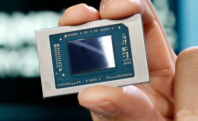
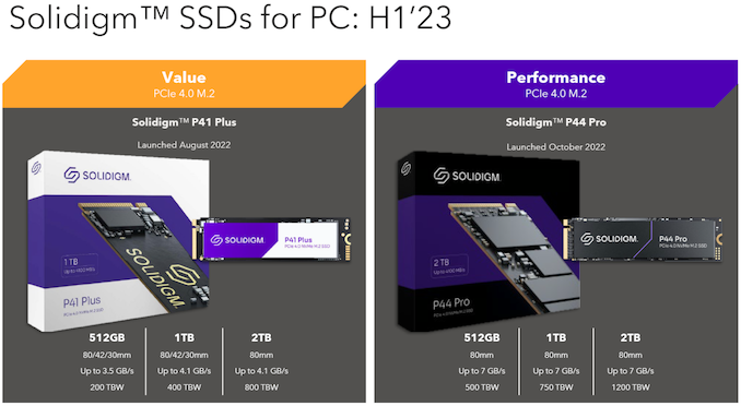
Solidigm has been active in the PC client SSD market with the QLC-based P41 Plus and the traditional TLC-based P44 Pro for the high-end market. While introducing the P41 Plus, Solidigm had also talked about the implementation of a read cache using the pSLC segment of the drive. This required the installation of Solidigm Synergy software. Over the last few quarters, the company has been hard at work perfecting the Solidigm Synergy 2.0 software release, with the promise of delivering even better performance for real-world workloads (compared to performance at launch) when used with the P41 Plus and the P44 Pro. While most SSD vendors work at the hardware and firmware levels, Solidigm believes there is performance benefits to be exploited at the software / driver level also.


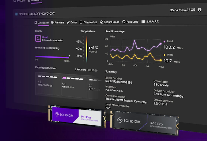
Solidigm’s Synergy 2.0 has two components – a Synergy Toolkit, and a Synergy Driver. While the toolkit taps into the SMART support and Windows performance counters and supports a variety of SSDs, the Synergy Driver is obviously supported only on Solidigm’s client SSDs.


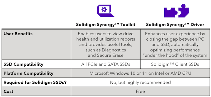
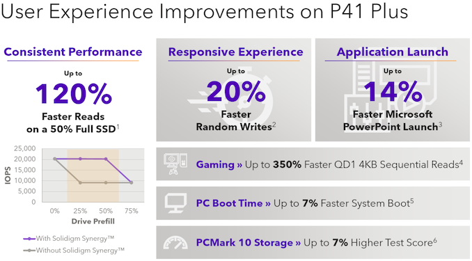
The toolkit itself is similar to the ones released by almost every other SSD vendor for the purpose of storage monitoring and maintenance. It collates a bunch of features that are spread over multiple tools and may be useful as a one-stop shop for mainstream users. The more interesting component is actually the Solidigm Synergy Driver that operates at the kernel level. Currently, this driver works only with Windows 10 or 11. Solidigm claims much better performance with its custom driver, with the QLC-based drive seeing significant improvement.


The driver is able to achieve this performance improvement using three different aspects:


  • Dynamic Queues
  • Prefetch for QD1 accesses
  • FastLane (host-managed caching)


Out of these three, FastLane is available only for the P41 Plus currently. This host-managed caching scheme was already discussed in detail in our launch coverage of the P41 Plus, though it didn’t have the FastLane moniker at that time.


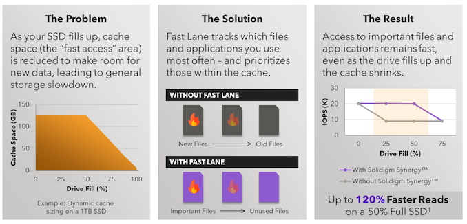
Read caching is of help only when the drive is not full enough to actually make the cache size too small to be of good use. Solidigm claims that this technique helps most in drives that are between 25% to 75% full


The Synergy Driver includes a feature that analyzes the storage trace of an application in real-time to detect predictable read operations. When the access queue depth is low and operations are sequential in nature, it is possible to predict the next access and prefetch it prior to the actual application request. This can increase responsiveness from an user experience perspective.


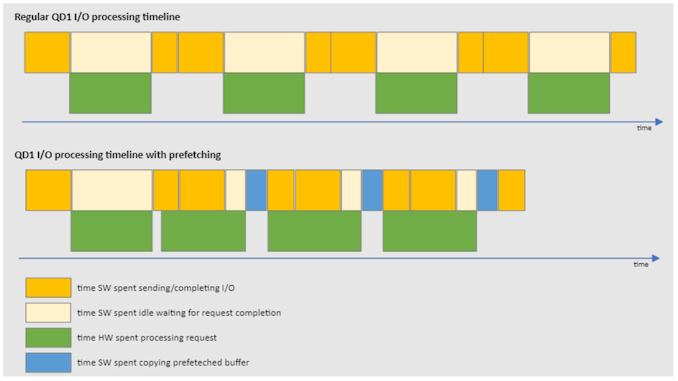
The driver allows up to 8 streams to be fetched, each with a buffer size of 512KB and maximum request size of 128KB. The driver’s prefetch behavior can be controlled via a registry parameter.


On systems with a large number of CPU cores, Solidigm claims that their driver can do a better job at routing I/O requests to relatively idle cores compared to the native Windows driver. The driver taps into the I/O request load, request size, and I/O processing times with / without CPU core redirection to decide whether to activate the dynamic queues. This process is dynamic – if the driver detects that the redirection makes completion times worse, or there is a change in workload, the dynamic queueing behavior is dropped. Similar to the smart prefetching, this aspect can also be deactivated using the registry.


Solidigm’s approach to delivering value additions to their client SSD customers after purchase is a marked departure from other vendors who rely solely on firmware updates – mostly for bug fixes. Providing better performance over time with driver releases is welcome from the end-user viewpoint. A point to keep in mind here is that these features help with real-world workloads – and not for use-cases primarily dealing with large sequential transfers, and measured using ATTO or CrystalDiskMark.


Source: AnandTech – Solidigm Synergy 2.0 Amplifies P41 Plus and P44 Pro Performance with Custom Driver

AMD Unveils Ryzen Mobile 7040U Series: Phoenix To Fly Into Thin Notebooks

Back at CES 2023, AMD announced a wave of upcoming Ryzen Mobile SKUs based on its Zen 4 silicon to launch in Q1 2023. Despite experiencing several delays in shipping its latest Ryzen Mobile 7040 silicon to partners and vendors, AMD has finally announced its line-up designed for thin and light notebooks, the Ryzen 7040U series. Featuring Zen 4 cores based on TSMC’s 4 nm process node, the AMD Ryzen 7040U series for mobile also includes AMD’s latest RDNA 3 graphics in the way of its Radeon 700M integrated graphics processor, with a varied TDP of between 15 and 30 W making these suitable for every day and run of the mill ultra-thin and light notebooks, while offering Zen 4 efficiency without looking to sacrifice too much on performance and features.


Source: AnandTech – AMD Unveils Ryzen Mobile 7040U Series: Phoenix To Fly Into Thin Notebooks

AMD: Ryzen Mobile 7040HS “Phoenix” Laptops to Reach Retailers in a Couple More Weeks

Alongside AMD’s usual slate of financial figures as part of their quarterly earnings call, the company also offered a brief update on the state of the next-generation Ryzen Mobile 7040HS “Phoenix” CPUs. After initially being slated for a March arrival – and then pushed back to April – the laptops are finally launching. According to AMD, the first systems should start arriving at retailers in the next few weeks.


First detailed during AMD’s CES 2023 keynote, the Ryzen Mobile 7040HS series (codename Phoenix) is AMD’s first mobile-focused, monolithic die CPUs based on the Zen 4 architecture, and will be their flagship silicon for mobile devices for 2023. Besides incorporating AMD’s latest CPU architecture, Phoenix also adds into the mix an updated RDNA3 architecture iGPU, and for the first time in any AMD CPU, a dedicated AI processing block, which AMD has aptly named the Ryzen AI. All of which, in turn, is fabbed using TSMC’s 4nm process – making it the single most advanced piece of silicon out of AMD yet.


AMD Ryzen 7040 Mobile CPUs

‘Phoenix’ on 4nm 
AnandTech C/T Base

Freq
Turbo

Freq
GPU GPU Freq L3 Cache

(MB)
TDP
HS-Series 35W – 54W
Ryzen 9 7940HS 8/16 4000 5200 RDNA 3

12 CUs
3000 16 35W – 54W
Ryzen 7 7840HS 8/16 3800 5100 RDNA 3

12 CUs
2900 16 35W – 54W
Ryzen 5 7640HS 6/12 4300 5000 RDNA 3

8 CUs
2800 16 35W – 54W


During a post-call Q&A with the press and analysts, AMD representatives offered an update on the state of 7040HS series processors, and the laptops they powered. According to AMD, the 7040HS series chips began ramping in Q1 – contributing to AMD’s client revenue for the quarter – and are now shipping to OEMs. As a result, AMD expects the first systems to hit retailers in the next couple of weeks.


If nothing else, the extended launch timeline underscores the difference between how AMD and arch rival Intel communicate product launches – and what they count as shipping. Whereas Intel’s massive client volume requires a large product ramp-up such that they’ll ship mobile chips to OEMs sometimes months before anything is announced, AMD has in recent years been satisfied to announce new mobile hardware well in advance of system availability. As a result, whether it’s intentional or not, most of the time AMD ends up defining a mobile launch as when chips are shipping to OEMs, rather than the availability of OEM systems. And that seems to be what has happened here.


For our part, back on April 30th AnandTech did find a single US retail listing claiming to have a Ryzen 7040HS laptop in stock. However, that listing from EXCaliberPC, for an ASUS ROG Zephyrus G14, now reads as a pre-order, with the retailer expecting it in stock on May 5th. Assuming they do receive systems on that day, then this would put the arrival of the very first systems a bit ahead of AMD’s latest projections – though still missing the previous claim of “OEM partners to launch the first notebooks powered by Ryzen 7040HS Series processors in April” by a week.


Ultimately, despite the delays in getting Phoenix out the door, AMD does have big plans for their first monolithic Zen 4 product. Besides serving as the cornerstone of their high-performance mobile offerings for the next year, Phoenix is also expected to be used in AMD’s Ryzen Z1 processors for handheld PC game consoles. And an eventual Ryzen Embedded product using the silicon is practically obigatory. So Phoenix will indeed rise high at AMD, eventually.


Source: AnandTech – AMD: Ryzen Mobile 7040HS “Phoenix” Laptops to Reach Retailers in a Couple More Weeks

AMD Reports Q1 2023 Earnings: Slipping Back into the Red as Client Sales Crumble

Continuing our earnings season coverage for Q1’2023, today we have the yin to Intel’s yang, AMD. The number-two x86 chip and discrete GPU maker has been enjoying a growing diet of Intel’s lunch for much of the past two years, but like the rest of the tech industry, AMD is now seeing a significant drop-off in sales as businesses and consumers alike curtail tech spending. So, like numerous other companies in this field, AMD has been bracing themselves for a rough first half of the year, after managing to beat the pack in Q4’2022 by posting a small profit.

For the first quarter of 2023, AMD reported $5.4B in revenue, continuing the year-over-year slide they’ve been experiencing throughout the past few quarters. All told, AMD’s top-line revenue dropped by 9% versus Q1’22, which is a much smaller drop than some of its rivals, but it’s a situation that has also been artificially buoyed by the Xilinx acquisition. That acquisition, which closed late into Q1’22, has boosted AMD’s revenue significantly on a year-over-year basis for the past few quarters – suffice it to say, it was not a small acquisition – though that is coming to an end now that AMD has owned Xilinx for over a full year.

The additional revenue and sales that Xilinx has brought to the table has shifted AMD in some important ways, but it hasn’t helped to halt the fundamental drop in sales that the tech industry is facing. As a result, the hit to AMD’s income has been significant; operating incomes dropped by 115% to negative $145M, and net income saw a similar dive into the red with a 118% drop, for a final tally of a $139M loss.


Source: AnandTech – AMD Reports Q1 2023 Earnings: Slipping Back into the Red as Client Sales Crumble

Intel PR Confirms Chip Branding Changes in the Works: Core i Series to Give Way to Ultra?

In an unusual move, Intel’s director of global communications, Bernard Fernandes, took to Twitter this morning to confirm that the chip giant is preparing some chip branding change for later this year. Citing that the company is at an “inflection point” ahead of the launch of their Meteor Lake architecture client CPUs later this year, Intel is apparently developing something new for branding their first mass-scale chiplet-based consumer CPU.


Yes, we are making brand changes as we’re at an inflection point in our client roadmap in preparation for the upcoming launch of our #MeteorLake processors. We will provide more details regarding these exciting changes in the coming weeks! #Intel


While the tweet in question doesn’t specifically address what it’s in response to, from context and timing it’s almost certainly a reaction to recent rumors that Intel is preparing to change their branding strategy for their Core family of consumer chips. And while it’s AnandTech policy not to republish or otherwise comment on rumors, an official comment from a high-ranking Intel PR representative means that this is no longer a mere rumor, and that changes are indeed in the works.


The current Core paradigm has been in place since late 2008 with the launch of the generational Core family and the now familiar i3/i5/i7 tiers. While Intel has since added the i9 tier and played with suffixes a few times in the last 15 years, Core branding has remained relatively consistent as a whole for what’s become 13 generations of parts.


But if the rumors are true, then the Core family will soon lose its i-series moniker. Based on benchmark data uploaded to the Ashes of the Singularity benchmark results database – a notorious source of leaks from hardware testers who neglect to turn off results reporting – an Intel Core Ultra 5 1003H has been spotted in the database. Which in turn implies that Intel is intended to phase out the Core i-series branding for new Core Ultra branding.


To be sure, Intel’s tweet does not confirm the Ultra branding; and Ashes alone is not a convincing source. But given that Intel has opted to confirm that they are making some brand changes to align with the Meteor Lake launch, if it’s not Ultra, then some other kind of branding change is clearly in the works.


Source: AnandTech – Intel PR Confirms Chip Branding Changes in the Works: Core i Series to Give Way to Ultra?

Microsoft To Stop Self-Branded PC Peripherals, Set to Focus on Surface Instead

Microsoft has confirmed that the company will discontinue selling PC accessories under the Microsoft brand, narrowing the firm’s focus to premium-priced peripherals sold under the Surface brand. The decision marks a major fork in the road for Microsoft-badged keyboards and mice, an era that started in 1983. And while the company isn’t going to cease the production of PC accessories entirely, the shift to Surface represents a much smaller scope in products going forward. This change, in turn, calls into question the future of ergonomic peripherals at Microsoft, a traditional niche for the company that has resulted in some of their best-known (and most beloved) PC accessories.


“Going forward, we are focusing on our Windows PC accessories portfolio under the Surface brand,” Dan Laycock, senior communications manager at Microsoft, told The Verge. “We will continue to offer a range of Surface branded PC Accessories — including mice, keyboards, pens, docks, adaptive accessories, and more. Existing Microsoft branded PC accessories like mice, keyboards, and webcams will continue to be sold in existing markets at existing sell-in prices while supplies last.”


The statement contradicts information published by Nikkei about Microsoft’s alleged plans to scale back production of Surface-branded gadgets. 


“We were recently informed by the client [Microsoft] to stop making stand-alone keyboards,” an executive at a Microsoft supplier reportedly told Nikkei. “We were told the Surface series will still be one of Microsoft’s development focuses, but just not the peripherals anymore.”​


Microsoft confirmation about its focus shift towards Surface-branded PC accessories comes several months after the company announced a change in its hardware portfolio, which was a part of some 10,000 job cuts. The PC market is struggling due to macroeconomic challenges and uncertainty among consumers. In fact, Microsoft’s own devices revenue, which includes Surface, PC accessories, and HoloLens, declined by 30% year-over-year in its most recent quarter, The Verge notes.


Microsoft-branded gadgets have been rather popular on the market over the past four decades, and while behind suppliers like Logitech, HP, and Dell, they’ve held their place – especially in the ergonomics market. Still, it has been getting increasingly hard for Microsoft to maintain its market share given the increasing number of players in the PC peripherals segment in general. The lucrative gaming keyboards and mice industry has been dominated by companies like Razer and Logitech for a while and then relatively new entrants like Corsair have not been making life of Microsoft any easier in the past decade with their highly-competitive products.


Surface-branded peripherals are a different segment though. They are not aimed at gamers and are not aimed at general users. Instead, they are designed for consumers willing to pay extra for advanced experience and businesses/enterprises for specific functionality. In fact, even Microsoft’s recently released Surface-badged Thunderbolt 4 hub is clearly designed for enterprise uses that need functionality like remote management.


Ultimately, although Microsoft is not exiting the peripherals market entirely, the company’s change in plans for the future of their hardware accessories seems to be much more significant than just a branding exercise. While Microsoft-designed mice, keyboards, and other devices will live on, narrowing their focus to premium, Surface-branded parts is a big change for a market that Microsoft has been a part of since almost the dawn of the PC – and likely not one for the better.


Source: AnandTech – Microsoft To Stop Self-Branded PC Peripherals, Set to Focus on Surface Instead

Matrox Adopts Intel Alchemist GPUs for New Luma Graphics Cards

While they’ve long since given up developing GPUs, Matrox has remained a notable player in the video card industry for over four decades. These days, the company has settled into a modest role of providing graphics cards based on other vendors’ GPUs for use in niche or boutique use cases, where Matrox can differentiate based on their software and support. And while their sales volume as a whole is limited, there’s a certain degree of validation that comes from Matrox tapping a vendor’s GPUs for their latest video cards.


To that end, Intel this week has finally earned their tip of the hat from the oldest of the video card vendors, with the announcement of a new series of multi-monitor display cards built around Intel’s Alchemist architecture GPUs. Matrox’s new Luma series graphics cards are based on Intel’s Arc A310 and A380 graphics hardware, with the niche video card maker looking to tap into the Alchemist’s class-leading video decoding and encoding capabilities, as well as the display output features and flexibility that are critical for a multi-display card.


Matrox Video’s Luma family of graphics boards includes three products: the full-sized single-slot Luma A380 based on the Arc A380 (ACM-G11 with 1024 stream processors) with 6GB of memory; the low-profile single-slot fanless Luma A310 based on the Arc A310 (ACM-G11 with 768 stream processors) with 4GB of memory; and the low-profile single-slot Luma A310F that is equipped with a active cooling system. 


All three Matrox Luma graphics cards have four DisplayPort 2.1 UHBR10 (40Gbps) outputs and thus can drive four 4Kp144/5Kp60 monitors (uncompressed, 4:4:4) or two 8Kp60 or 5Kp120 displays using two of such ports for each displays. As for features, they offer the same capabilities as other Intel Arc A310/A380-based offerings, including support for DirectX 12 Ultimate, OpenGL 4.6, Vulkan 1.3, and OpenCL 3.0 APIs, as well as encoding and decoding of H.264, H.265, VP9, and AV1 video streams. As an added bonus, they retain support for Intel’s oneAPI for compute tasks, as well as the Intel Distribution of OpenVINO toolkit for AI development.


All of the Luma graphics cards consume no more than 75W and can be powered entirely via a PCIe slot without any auxiliary power connectors, and the A310-based offerings are intended to fit into the most compact PCs that are out there. Furthermore, their single-slot design means that upwards of several cards can be installed into a single desktop PC for systems that need to drive eight, 12, or more monitors.


Meanwhile, it’s interesting to note that while Matrox has not announced the discontinuation of their previous generation cards for these product segments – the NVIDIA based D-series and AMD-based M-series – in terms of specifications these new Intel cards should supplant the older cards in every way. Intel’s DisplayPort 2.1 capabilities are likely the driving factor given Matrox’s intended niche, with NVIDIA in particular being boxed out by not including DisplayPort 2.1 functionality with their Ada Lovelace generation GPU architecture.


Matrox Video’s Luma boards are aimed primarily at the medical, digital signage, control room, video wall, and industrial markets. The cards come with a base three-year warranty, which can be further extended and a guaranteed lifecycle of seven years, which is important for some of the markets that they are intended for. 


Other advantages Matrox’s Luma board offer include support for Matrox’s PowerDesk software developed to handle exotic multi-display configurations. 


Matrox did not announce prices of the boards, though given their orientation on commercial, professional, and industrial applications, they will be priced accordingly.


Source: AnandTech – Matrox Adopts Intel Alchemist GPUs for New Luma Graphics Cards

Intel Reports Q1 2023 Earnings: A Record Losing Quarter Goes Better Than Expected

Kicking off our coverage of the first earnings season of the year for the tech industry, we as always start with Intel. The blue-hued blue-chip is the first out of the gate to report their results for the first quarter of 2023, with Intel picking up the pieces after a rough end to 2023, and a rather painful start to 2023. With revenue down on a yearly basis almost across the entire board thanks to a major, industry wide slump in client and server sales, Intel’s focus has been on battening down the hatches to weather this rough period, while preparing for an eventual (if modest) upturn in the market later this year.

For the first quarter of 2023, Intel booked $11.7B in revenue, a precipitous 36% drop from the year-ago quarter. As was the case in Q4, Intel is in the midst of a major industry slump, which has hit revenues hard and operating/net incomes even harder. Intel closed the quarter in the red on an operating income basis, losing $1.5B, and the company’s overall net loss was a staggering $2.8B on a GAAP basis.


Source: AnandTech – Intel Reports Q1 2023 Earnings: A Record Losing Quarter Goes Better Than Expected

TSMC Announces Early Access Nodes for Next-Gen Car Chips: N4AE and N3AE

As the final set of announcements from this week’s North American Technology Symposium, TSMC closed out their fab roadmap updates with some fresh news on their automotive-centric processes. For their automotive customers, TSMC is gearing up to deliver a pair of new specialized process nodes for the market, N4AE and N3AE, which are aimed at delivering early versions of TSMC’s forthcoming automotive-grade process nodes for use by clients who need to get an early start with design and/or production.


The automotive industry is notoriously conservative when it comes to chip manufacturing, as automotive products are expected to meet a much higher bar in terms of safety and reliability. For good reason, the automotive industry is traditionally a generation or so behind in terms of the silicon lithography process nodes used, as they wait for them to become truly proven processes. With that said, the trend towards software-defined vehicles is driving a quick ramp-up in demand for more performant processors – and more chips altogether – which has been spurring the industry to close the gap a bit and transition to newer nodes sooner.


In order to meet that expected demand, this week TSMC announced its Automotive Early (AE) fabrication processes, which are aimed at helping automakers start earlier on the design of new chips for leading-edge nodes. Essentially stepping-stone nodes along the path to developing a full, automotive-grade N3A process, TSMC’s N3AE (3nm class) and N4AE (4nm class) technologies are slated to offer consumer-grade reliability and will come with automotive-specific process design kits (PDKs) based on N3E and N4P respectively.


For customers who need a traditional, high-reliability automotive-grade chip, N3AE can be used by chip designers later this year to start developing automotive grade products that, in turn, will be fabbed on the fully-qualified automotive-grade N3A production node in a couple of years. Alternatively, customers who want to bring  chips to the market sooner to drive less critical systems in a car – such as digital cockpits and other non-critical systems – can plan to go into production with N4AE. Production on an Automotive Early node means forgoing some of the benefits of a fully qualified automotive process node – essentially building chips that are closer to consumer grade – but it will allow chip designers to get their chips in production on cutting-edge nodes upwards of a year sooner.


Traditionally, automakers and developers of automotive-grade electronics demanded their chips to be qualified for quality and reliability both in terms of functional safety (classified by ASIL system) and physical robustness (classified by AEC-Q100 standards). Improving the physical robustness of chips requires process technologies and design rules that have been specifically developed/tweaked meet those higher requirements, and typically it takes foundries and their automotive chip partners two or three years to develop an automotive-grade process technology. For example, TSMC has been making chips for smartphones and PCs on its N5 (5nm-class) fabrication process since 2020, but automotive grade N5A is only finally set to be ready this year.


At the same time, not all systems inside a vehicle need to comply with the most stringent integrity and reliability standards. For example, chips powering infotainment, digital cockpit, and advanced driver assistance systems (ADAS) do not have to be AEC-Q100 Grade 1 (handle temperatures between -40°C and +150°C). These systems also tend to require a lot of processing horsepower, leading to them significantly benefiting from leading-edge nodes.


TSMC said that its N3AE (3nm Auto Early) will be launched in 2023 and will provide automotive process design kits (PDKs) based on N3E. It will enable customers to initiate designs on the 3nm node specifically for automotive applications, ultimately leading to the N3A process, which is expected to be fully qualified for automotive use in 2025.


Meanwhile, customers in more of a hurry will also have N4AE as an option. N4AE is based on TSMC’s existing N4P process technology, and customers will be able to start risk production on N4AE a year sooner, in 2024. Presumably, given its heritage from N4P, N4AE would also be a good candidate for incorporating IP already designed for N4P (which there is already piles of), further reducing the time to market.


TSMC did not touch upon which of its customers are interested in using its N3AE and N4AE process technologies for their automotive SoCs, but there are several usual suspects that have been offering high-performance feature-rich automotive SoCs for years.


Source: AnandTech – TSMC Announces Early Access Nodes for Next-Gen Car Chips: N4AE and N3AE

Intel: Meteor Lake & Intel 4 Process Now Ramping for Production

As part of today’s Q1’2023 earnings announcement from Intel, the company is offering a brief update on the state of its upcoming chips and manufacturing nodes. Key among these disclosures is a status update on Meteor Lake, Intel’s next-generation client processor (and first disaggregated chiplet CPU), as well as the Intel 4 process node that it will be built upon.


According to Intel, the company is on track to launch Meteor Lake in the second half of the year. And more specifically, at this point Meteor Lake is now in production and ramping alongside the new Intel 4 process.


“CCG’s Meteor Lake product on Intel 4 is ramping production wafer starts for an expected launch in the second half of 2023.”


The basis of what we expect will be sold as Intel’s 14th generation of Core processors, Meteor Lake is a critical part for Intel that represents several firsts for the company. It’ll be the first client CPU using chiplets, but also the first heterogenous chiplet CPU from the company, using different chiplets for I/O, CPU cores, graphics, and more. And on the manufacturing side of matters, it’s going to be the lead product for Intel’s next-generation EUV-based Intel 4 process node, as well as Intel’s biggest use of Foveros 3D die stacking technology yet – and the first attempt to do so for a relatively cheap, mass-market processor.


Intel’s last significant update on Meteor Lake came almost exactly a year ago, when the company announced during their Q1’2022 earnings report that it had been successfully powered on for testing. So at a year later, Intel is now making final preparations for a product launch later this year. The official launch window is still in the second half of the year – Intel client processor ramp-ups take several months even without all-new manufacturing technologies in play – so we expect Intel will announce more concrete details on that launch some time in the third quarter.


Source: AnandTech – Intel: Meteor Lake & Intel 4 Process Now Ramping for Production

AMD Issues Second Statement on Ryzen 7000 Burnout Issues: Caps SoC Voltages

Yesterday, AMD issued a statement surrounding the issues some users have been experiencing with their Ryzen 7000X3D processors. The problem reported widely across Reddit subforums, includes some Ryzen 7000X3D CPUs burning the CPU socket on AM5 motherboards and damaging the chips, rendering them dead. AMD has released a second statement regarding the issue, including what it is doing to rectify the problem and subdue any panic users and owners of the Ryzen 7000 series processors.


The official statement from AMD is as follows:


We have root caused the issue and have already distributed a new AGESA that puts measures in place on certain power rails on AM5 motherboards to prevent the CPU from operating beyond its specification limits, including a cap on SOC voltage at 1.3V. None of these changes affect the ability of our Ryzen 7000 Series processors to overclock memory using EXPO or XMP kits or boost performance using PBO technology.

We expect all of our ODM partners to release new BIOS for their AM5 boards over the next few days. We recommend all users to check their motherboard manufacturers website and update their BIOS to ensure their system has the most up to date software for their processor. 


Anyone whose CPU may have been impacted by this issue should contact AMD customer support. Our customer service team is aware of the situation and prioritizing these cases.


To counteract the problem, AMD has seemingly identified an issue with voltages going too high when users enable AMD’s EXPO memory profiles. The cap on SoC voltages looks to be the primary change in the AGESA firmware rollout, although AMD has identified a possible voltage rail within the CPU that is causing the burnouts. Along with SoC voltages, AMD has put a limit within the firmware that prevents the Ryzen 7000 CPUs from going beyond specification.


Enabling EXPO memory profiles on compatible DRAM looks to be pushing SoC voltages beyond AMD’s safe spot on the Ryzen 7000 processors, which AMD believes is the root cause of the burning issue.


One interesting point about AMD’s statement is that it eludes to whether or not the issue is just on its Ryzen 7000X3D processors or whether it affects all of its Ryzen 7000 processors entirely. Regardless of the Zen 4 chip that users may have, AMD is ambiguous in its language, and it seems to be that AMD is recommended that ALL users with a Ryzen 7000 series processor should update to the latest firmware.


AMD is actively working with its motherboard partners to release a new AGESA firmware, which they say has already been distributed, limits the SoC voltage to 1.30 V. AMD claims that all AM5 motherboard vendors and models should have a new BIOS version available to them within the next few days, and is recommending all users to update their BIOS at their earliest convenience.


Image source: Speedrookie/Reddit


Source: AnandTech – AMD Issues Second Statement on Ryzen 7000 Burnout Issues: Caps SoC Voltages

TSMC Details 3nm Evolution: N3E On Schedule, N3P and N3X To Deliver 5% Performance Gains

Alongside some new announcements for their 2nm process node plans, TSMC has also released a progress and roadmap update for their N3 family process technologies at today’s 2023 North American Technology Symposium. TSMC’s final generation of FinFET-based process nodes, the N3 family is expected to remain around in some shape or form for many years to come as the densest node available for customers who don’t need a more cutting-edge GAAFET-based process.


TSMC’s big roadmap updates on the N3 front were with N3P and its high performance variant, N3X. As revealed today by TSMC, N3P will be an optical shrink of N3E, offering enhanced performance, reduced power consumption, and increased transistor density compared to N3E, all while maintaining compatibility with N3E’s design rules. Meanwhile, N3X will wed extreme performance with 3nm-class densities, offering higher clockspeeds for high performance CPUs and other processors.


N3E: 3nm for Everyone Is on Schedule


As a quick refresher, TSMC’s N3 (3nm-class) family of process technologies is comprised of several variants, including baseline N3 (aka N3B), relaxed N3E with reduced costs, N3P with enhanced performance and chip density, and N3X with higher voltage tolerances. Last year the company also talked about N3S with maximized transistor density, but this year the company remains tight lipped about this node and it is not mentioned anywhere in its slides.


TSMC’s vanilla N3 node features up to 25 EUV layers, with TSMC using EUV double-patterning on some of them to make for higher logic and SRAM transistor density than N5. EUV steps are expensive in general, and EUV double patterning drives those costs up further, which is why this fabrication process is only expected to be used by a handful of customers who are not as concerned about the high outlay required.


Advertised PPA Improvements of New Process Technologies

Data announced during conference calls, events, press briefings and press releases
  TSMC
N3

vs

N5
N3E

vs

N5
Power -25-30% -32%
Performance +10-15% +18%
Logic Area


Reduction* %


Logic Density*
0.58x


-42%


1.7x
0.625x


-37.5%


1.6x
SRAM Cell Size 0.0199µm² (-5% vs N5) 0.021µm² (same as N5)
Volume

Manufacturing
Late 2022 H2 2023


The majority of TSMC’s clients interested in a 3nm-class process are expected to use the relaxed N3E node, which according to TSMC is on schedule and achieving their performance targets. N3E uses up to 19 EUV layers and does not rely on EUV double patterning at all, reducing its complexity and costs. The trade-off is that N3E offers lower logic density than N3, and it has the same SRAM cell size as TSMC’s N5 node, making it somewhat less attractive to those customers who are driving for density/area gains. Overall, N3E promises a wider process window and better yields, which are two crucial metrics in chip fabrication.


“N3E will be better than N3 in terms of yield, process complexity, which directly translating into [wider] process window,” said Kevin Zhang, Vice President of Business Development at TSMC. 


N3P: Higher Performance, Higher Transistor Density


Following N3E, TSMC will continue to optimize the N3 family’s transistor density with N3P, which will build on N3E by offering improved transistor characteristics. The refined process node will allow chip designers to either increase performance by 5% at the same leakage or reduce power by 5% ~ 10% at the same clocks. The new node will also increase transistor density by 4% for a ‘mixed’ chip design, which TSMC defines as a chip consisting of 50% logic, 30% SRAM, and 20% analog circuits.


As part of their discussion on N3P, TSMC stressed that the density improvement was achieved by adjusting the optical performance of its scanners. So it is likely that TSMC will be able to shrink all types of chip structures here, which will make N3P an attractive node for SRAM-intensive designs.


“N3P is a performance boost, it has a 5% higher performance, at least a 5% higher than N3E,” explained Zhang. It also has the 2% optical shrink, which bring transistor density to 1.04x.”


Advertised PPA Improvements of New Process Technologies

Data announced during conference calls, events, press briefings and press releases
  TSMC
N3

vs

N5
N3E

vs

N5
N3P

vs

N4E
N3X

vs

N3P
Power -25-30% -32% -5% ~ 10% higher
Performance +10-15% +18% +5% +5%

Fmax @ 1.2V
Chip Density ? ?    
SRAM Cell Size 0.0199µm² (-5% vs N5) 0.021µm² (same as N5) ? ?
Volume

Manufacturing
Late 2022 H2 2023 H2 2024 2025


Since N3P is an optical shrink of N3E, it will preserve N3E’s design rules, enabling chip designers to quickly reuse N3E IP on the new node. Consequently, N3P is also projected to be one of TSMC’s most popular N3 nodes, so expect IP design houses like Cadence and Synopsys to offer a variety of IP for this process technology, reaping the benefits of forward compatibility with existing N3E in the process. TSMC says that N3P will be production ready in the second half of 2024.


N3X: Maximum Performance and Density


Finally, for developers of high-performance computing applications like CPUs and GPUs, TSMC has for the past few generations been offering its X family of high voltage, performance-focused nodes. As disclosed at last year’s event, the N3 family will be getting its own X variant with the aptly named N3X node.


Compared to N3E, N3X is projected to offer at least 5% higher clockspeeds compared to N3P. This is being accomplished by making the node more tolerant of higher voltages, allowing chip designers to crank up the clockspeeds in exchange for higher overall leakage.


TSMC claims that N3X will support voltages of (at least) 1.2v, which is a fairly extreme voltage for a 3nm-class fabrication process. The leakage cost, in turn, is significant, with TSMC projecting a whopping 250% increase in power leakage over the more balanced N3P node. This underscores why N3X is really only usable for HPC-class processors, and that chip designers will need to take extra care to keep their most powerful (and power-hungry) chips in check.


As for transistor density, N3X will offer the same density as N3P. TSMC has not commented on whether it will also maintain design rule compatibility with N3P and N3E, so it will be interesting to see what ends up happening there.


The final N3 family node in TSMC’s current roadmap, the company says that that N3X will be production ready in 2025.


Source: AnandTech – TSMC Details 3nm Evolution: N3E On Schedule, N3P and N3X To Deliver 5% Performance Gains

TSMC Outlines 2nm Plans: N2P Brings Backside Power Delivery in 2026, N2X Added To Roadmap

At its 2023 North American Technology Symposium today, TSMC has disclosed additional details about its plans for its forthcoming N2 2nm-class production nodes in 2025 – 2026 and beyond. TSMC’s N2 family of fabrication technologies will be expanding with additional variations, including N2P with backside power delivery, and N2X for high-performance computing. Between these forthcoming N2 generation process nodes, TSMC is laying out a roadmap to continue their relentless pace of increasing transistor performance efficiency, optimize power consumption, and improving transistor density.


Source: AnandTech – TSMC Outlines 2nm Plans: N2P Brings Backside Power Delivery in 2026, N2X Added To Roadmap

Report: DDR5 RDIMM Production Impacted by PMIC Compatibility Issues

Memory module producers have been shipping unbuffered DDR5 memory modules for desktop and laptop computers running Intel’s 12th Generation Core ‘Alder Lake’ processors in high volumes since September, 2021, without any major issues. But DDR5 is just now entering the datacenter world, and according to a recent report, it looks like power management ICs (PMICs) for registered DIMMs have become a constraining factor due to compatibility issues.


In a report published by TrendForce discussing the current state of the market for server-grade DDR5 memory, the semiconductor analyst firm noted that there is an issue with PMIC compatibility for DDR5 RDIMMs, with both DRAM suppliers and PMIC vendors are collaborating to resolve the problem. The analysts do not reveal the exact root cause of the problem, but claim that PMICs from Monolithic Power Systems (MPS) do not have any issues, leading them to expect MPS PMICs to be in high demand for the foreseeable future.


Although DRAM makers have been distributing samples of their server grade modules to CPU and server makers since early 2022, practical issues only emerged recently when producers began to ramp up production of their machines running AMD’s EPYC 9004 ‘Genoa’ and Intel’s 4th Generation Xeon Scalable ‘Sapphire Rapids’ processors. As a result, the demand for PMICs from a single supplier has created a bottleneck in production, claims TrendForce. This will have a knock-on effect on the server market, which is already suffering from a demand drop.


Neither analysts nor DRAM producers are currently disclosing the precise reason for the PMIC issue. But it is evident that, as both client and server DDR5 DIMMs require PMICs, it is turning out to be harder to make server-grade modules than client-aimed DIMMs.


As part of the changes that came with the DDR5 specification, DDR5 memory modules now come with their own voltage regulating modules (VRMs) and PMIC. Moving these components on to DIMMs is intended to minimize voltage fluctuation ranges (DDR5’s allowable range is about 3% (±0.033V) for a 1.1 volt supply), as well as decrease power consumption and improve performance. But doing so adds complexity to individual DIMMs, as well. 


Unbuffered DDR5 DIMMs for client PCs are relatively simple since they are all single or dual-rank and carry at most 16 single-die memory chips. High-capacity Registered DDR5 memory modules for servers use more chips and those chips can pack in multiple DRAM dies each, which greatly increases complexity.


As a result of the PMIC bottleneck as well as a slower ramping of DDR5 manufacturing capacity, TrendForce predicts that prices of server-grade 32GB DDR5 modules will drop to around $80 – $90 in April and May, due to the lower fulfillment rates of DDR5 server DRAM in the short term. As a result, DDR5 prices are expected to fall more slowly than DDR4 for the next couple of quarters, with DDR5 prices only finally catching up (or rather, down) with DDR4 once production picks up.


Source: AnandTech – Report: DDR5 RDIMM Production Impacted by PMIC Compatibility Issues

Corsair Launches MP600 Mini: M.2 2230 SSD Brings Big Performance

Corsair has introduced its first ever SSD in an M.2-2230 form-factor that is aimed at ultra-compact systems like Valve’s Steam Deck as well as Microsoft’s Surface Pro 8 and 9. The MP600 Mini drive delivers 1 TB of storage space and strong performance in a miniature package.


Corsair’s MP600 Mini is based around Phison’s E21T controller mated with 3D TLC NAND memory (according to Tom’s Hardware) and is rated with an up to 4,800 MB/s sequential read/write speed as well as an up to 850K/1.1M random read/write IOPS. The SSD consumes about 4.3W on average and comes with a simplistic graphene heatspreader, which makes it compatible with the vast majority of systems out there.


Since Corsair’s MP600 Mini uses a PCIe 4.0 x4 interface, it will shine in the vast majority of modern laptops and hybrid PCs. Though as far as Valve’s Steam Deck is concerned, keep in mind that it uses a PCIe 3.0 x4 interface, so the MP600 Mini won’t get to fully stretch its legs there in terms of throughpt.


Corsair MP600 Mini Specifications
Capacity 1 TB
Form Factor M.2 2230
Interface PCIe Gen4 x4, NVMe 1.4
Controller Phison PS5021-E21T
NAND Flash 3D TLC
Sequential Read 4800 MB/s
Sequential Write 4800 MB/s
Random Read 850k IOPS
Random Write 1100k IOPS
Endurance 600TBW
Warranty 5 Years
Power Active 4.3 W
Idle 5 mW


The market for retail M2.2230 SSDs has traditionally been a small one, owing to the limited use of the drives in user-upgradable machines. However the recent launch of the Steam Deck in particular has kicked up significant demand for these SSDs – especially high-performance drives befitting a game console. So Corsair’s MP600 Mini is a welcome addition to the space. 


Corsair currently sells its MP600 Mini directly for $110, which might seem expensive for a 1 TB drive, but keeping in mind that we are dealing with a pretty fast model that comes in an M.2-2230 form-factor (a rare combination), the price is consistent with similar drives.


Source: AnandTech – Corsair Launches MP600 Mini: M.2 2230 SSD Brings Big Performance

AMD Releases Ryzen Z1 Series: Zen 4 & RDNA 3 Come To Handheld Game Consoles

AMD has announced the Ryzen Z1 series of high-performance processors for handheld PC gaming consoles. The latest Ryzen Z1 chips wield Zen 4 cores and RDNA 3 graphics, a familiar combination that AMD uses for its current mobile Ryzen 7040HS series (Phoenix) processors. And while the chipmaker hasn’t officially announced any lower power Phoenix chips yet (e.g. Ryzen 7040U series), given the similarities in the feature set of the Ryzen Z1 family and the Phoenix silicon, the Ryzen Z1 series appears to be a custom-tailored Phoenix SKU that prioritizes energy efficiency for handheld gaming devices, with the lead customer being Asus and their upcoming ROG Alloy.


The Ryzen Z1 series is being introduced with two SKUs. The top-tier Ryzen Z1 Extreme has eight Zen 4 CPU cores – the maximum found on Phoenix – while the vanilla Ryzen Z1 cuts that down to six CPU cores. Meanwhile on the graphics side of matters, the Ryzen Z1 Extreme flaunts 12 RDNA 3 architecture compute units, again aligning with the max number found on Phoenix silicon. It’s vanilla Z1 counterpart, on the other hand, will ship with just 4 CUs enabled, one-third as many as on the flagship part.


Both chips benefit from a 16 MB L3 cache, while the Ryzen Z1 Extreme has 2 MB more L2 cache due to its additional CPU cores. In any event, the Ryzen 1 and Ryzen Z1 Extreme possess strong computing performance thanks to the high CPU core count and the usage of AMD’s latest Zen 4 cores. A hexa-core processor should suffice for handheld gaming, and either Ryzen Z1 processor will certainly outperform AMD’s older custom quad-core Zen 2 SoC (Aerith) that powers Valve’s Steam Deck.


AMD Ryzen Z1 Specifications
AnandTech Cores

Threads
Base

Freq
Turbo

Freq
L2

Cache
L3

Cache
GPU TDP
Ryzen Z1 Extreme 8/16 ? ? 8 MB 16 MB 12 RDNA 3 CUs 15 – 30 W
Ryzen Z1 6/12 ? ? 6 MB 16 MB 4 RDNA 3 CUs 15 – 30 W


Hardware unit counts aisde, AMD isn’t revealing the clock speeds for the two 4nm processors. Curiously, an embargoed report published by The Verge has quoted “up to” 8.6 TFLOPS and 2.6 TFLOPS graphics performance respectively, based on AMD’s engineering projections. But these figures have been removed from the deck AMD has since been sending around to the rest of the press. If these figures do turn out to be reasonably close to what the final shipping silicon can hit, then that would mean we’d be looking at peak GPU clockspeeds of around 2.8GHz and 2.6GHz respectively, which is just a bit lower than what the Ryzen 7040HS chips run at.


The Ryzen Z1 series chips will support a maximum TDP of 30 Watts, which happens to be the same top power target as AMD’s mobile Ryzen U-series chips. Meanwhile, although this wasn’t in AMD’s press deck or press release, AMD’s Ryzen Z1 product page lists a minimum TDP of 15 Watts. Though it’s worth noting that unlike TDP maximums, TDP minimums are not a hard floor or ceiling for mobile processors. Chips can be configured to run even less when it’s called for, depending on what the customer desires.


Just to offer a comparison here, Aerith’s TDP is between 4 W and 15 W, meaning the Z1 series certainly offers a good deal larger power range for customers to play with. At its top TDP, such a configuration would quickly blow through the battery in any handheld device, but for docked devices it’s very feasible. As for handheld mode, it’s far more likely that we’ll see Z1 chips clocked relatively low to conserve precious power.


Being that this is an AMD product designed for PC-like devices, it has access to all AMD graphics technologies, including Radeon Chill, which helps improve battery life by adjusting frame rates based on the movements in the game. This also means that FSR will be on the table on a game-by-game basis, and RSR as a less optimal universal solution.


AMD provided some benchmarks for the Ryzen Z1 series utilizing the Asus ROG Ally. As usual, throw a pinch of salt over vendor-provided benchmarks. The device used here also had 16 GB of LPDDR5 memory and a Micron 500 MB SSD. It’s important to highlight that AMD put the Asus ROG Alloy in turbo mode for its benchmarks, which means that the Ryzen Z1 series processors were operating at power levels up to 30 Watts.


AMD’s results show the Ryzen Z1 Extreme delivers average frame rates above 60 FPS in most titles. However, the chipmaker tested with the lowest settings at a mix of 1080p and 720p upscaled with RSR to hit those figures. The Ryzen Z1’s performance wasn’t bad, but the two chips’ delta was perceptible. The difference spans between 6% and 73%. Zen 4-based processors took a significant performance hit at native 1080p resolution on the lowest settings. As expected, the Ryzen Z1 struggled in multiple titles and didn’t hit the 60 FPS mark. 


Asus has first dibs on the Ryzen Z1 series; however, more competitors powered by the 4nm Ryzen Z1 chips should arrive down the road. Asus’ ROG Ally will be the first handheld gaming console to feature AMD’s Ryzen Z1 Extreme processor, with the company set to share more information on the handheld (including pricing) on May 11.


Source: AnandTech – AMD Releases Ryzen Z1 Series: Zen 4 & RDNA 3 Come To Handheld Game Consoles

ASUS Issues Statement on Ryzen 7000X3D Processor Issues, Possible Voltage Issues with AMD EXPO

Yesterday we reported that MSI announced a wave of firmware updates designed to address and alleviate potential issues with users on AM5 using AMD’s Ryzen 7000X3D processors with 3D V-Cache. One of the main changes with MSI’s latest UEFI firmware for AM5 included voltage restrictions when using Ryzen 7000X3D series CPUs so that these chips couldn’t be overvolted as the V-Cache packaging is somewhat sensitive to additional power.


Further to MSI’s announcement, ASUS has released a statement to experienced engineer and extreme overclocker Roman ‘Der8auer’ Hartung, which addresses the potential issue with using AMD’s EXPO memory profiles in conjunction with the Ryzen 7000X3D series chips. One of the key elements that seemingly surrounds the problem is the use of AMD’s EXPO memory overclocking profiles.


ASUS’s Director of Global Product Marketing and Technical Marketing, Rajinder Gill, said in a statement to Der8auer, “The EFI updates posted on Friday contain some dedicated thermal monitoring mechanisms we’ve implemented to help protect the boards and CPUs. We removed older BIOSes for that reason and also because manual Vcore control was available on previous builds.” Rajinder also said, “We’re also working with AMD on defining new rules for AMD Expo and SoC voltage. We’ll issue new updates for that ASAP. Please bear with us.


ASUS ROG Crosshair X670E Hero AM5 Motherboard for AMD Ryzen 7000 Series CPUs


Looking at the narrative of the statement provided to Der8uaer from Rajinder, we can confirm that ASUS has indeed removed older iterations of its firmware for its AM5 motherboards. Looking at the EMEA side of things, at the time of writing, the latest firmware update to be posted on the ASUS product pages is dated 04/21/2023, which indicates ASUS recently updated the firmware, but the update isn’t the latest one in question.


Roman ‘Der8auer’ Hartung’s Ryzen 9 7900X also has a bulge.


The one thing these issues have in common is that AMD’s EXPO memory profiles have been applied, claims Roman ‘Der8auer’ Hartung, and even highlighted that his Ryzen 9 7900X processor also fell foul the the ‘bulging issue.’ This is particularly interesting as this isn’t an X3D series chip with 3D V-Cache, although we’re not aware of any other reports of non-X3D Ryzen 7000 chips being affected at this time.


Enabling EXPO memory profiles on Ryzen 7000 processors does several things to the processor that pushes it beyond the technical specification of the chip. Chief among these is raising the SoC voltage and some other primary voltages, such as VDDIO, which are used to feed the IOD. Like any ASIC, there are limits to how high voltages can be safely pushed, and this is one theory behind the cause of the recent run of damaged Ryzen reports. Though how this might be connected to the issue being centered around Ryzen X3D chips – where the voltage-sensitive V-Cache is on the CCDs and their separate voltage plane – is unclear at this time.


In any case, this does underscore why AMD’s EXPO memory overclocking profiles void the warranty on these chips, as there’s more to EXPO than just ramping up memory frequencies and applying more voltage to the DRAM itself.


Further to Rajinder’s statement given to Der8auer, ASUS’s Senior Technical Marketing Manager, Juan Jose Guerrero, posted the following statement on Twitter Tuesday afternoon:


“Several AMD Ryzen 7000X3D owners have reported CPU and motherboard failures. We acknowledge the incidents/issues and have been communicating with AMD to analyze the possible causes. We have also contacted affected users to provide support and collect additional information.


Ryzen 7000X3D processors do not allow for CPU ratio or CPU core voltage tuning (CPU overclocking) but do allow for performance tuning and DRAM overclocking via PBO2 and EXPO memory. To support EXPO and/or memory overclocking at DDR5-6000 and beyond, SoC voltage has to be sufficiently increased to ensure compatibility and stability. The amount of voltage required varies between CPU samples. Some processors are more sensitive to overvoltage than others, and some are capable at running higher memory frequencies without needing as much voltage.


As confirmed with AMD, any intentional manipulation of these settings can damage the processor, socket, and motherboard. To mitigate this, we have been working with AMD to define new rules for EXPO memory and SoC voltage. To help protect the CPU and motherboard, we are issuing new EFI updates to limit the maximum available SoC voltage to 1.3V.


We recommend updating your motherboard UEFI BIOS to the latest release. Please also ensure the CPU is cooled adequately. Our recommendation is to use at least a 240mm AIO liquid cooler or high-performance air cooler. If you have been affected, please do not hesitate to contact ASUS support for your region.


As we mentioned in our article yesterday about MSI addressing CPU voltage on their own AM5 motherboards, vendors are looking to address any more potential issues, following a small-but-concerning number of reports circulating on Reddit that their Ryzen 7000X3D processors are burning out and killing the motherboard in the process. ASUS’s statement and the summary of the firmware on the official product page indicate that ASUS is worried about SoC voltage, and as such, the new firmware locks it down to 1.30 V. Which ASUS states is to ‘protect the CPU and motherboard.’ 


Screenshot of the ROG Crosshair X670E Extreme BIOS/Support page on the official product page (China).


On the Chinese product page for the ROG Crosshair X670E Extreme, the firmware has been updated as of today (at the time of writing) to 04/25/2023, and the firmware version in question (1302) does seemingly address the SoC voltage.


Further to ASUS’s and MSI’s statements, AMD has officially responded with a statement of their own:


It reads, “We are aware of a limited number of reports online claiming that excess voltage while overclocking may have damaged the motherboard socket and pin pads. We are actively investigating the situation and are working with our ODM partners to ensure voltages applied to Ryzen 7000X3D CPUs via motherboard BIOS settings are within product specifications. Anyone whose CPU may have been impacted by this issue should contact AMD customer support.”


Of course, these issues of Ryzen 7000X3D series processors burning out aren’t just limited to those using MSI and ASUS motherboards. Since the initial reports, users have reported additional issues on various models and brands across threads on Reddit. The potential for damage is one of the primary reasons AMD locked down the X3D series processors so that users couldn’t manually overclock them. Even the first iteration, the Ryzen 7 5800X3D, was also locked down.


One thing remains clear: AMD and its motherboard partners are now officially investigating the matter, and users with affected Ryzen 7000 CPUs are advised to contact AMD customer support directly.


Source: AnandTech – ASUS Issues Statement on Ryzen 7000X3D Processor Issues, Possible Voltage Issues with AMD EXPO

AMD Issues Official Statement on Reported Ryzen 7000 Burnout Issues

Yesterday we reported that MSI announced a wave of firmware updates designed to address and alleviate potential issues with users on AM5 using AMD’s Ryzen 7000X3D processors with 3D V-Cache. One of the main changes with MSI’s latest UEFI firmware for AM5 included voltage restrictions when using Ryzen 7000X3D series CPUs. Further to recent reports of users with AMD Ryzen 7000X3D processors experiencing damage to their chip and motherboard socket, we reached out to AMD this morning to seek clarification. AMD has just responded with an official statement concerning the current problem.


The statement directly from AMD is as follows:


“We are aware of a limited number of reports online claiming that excess voltage while overclocking may have damaged the motherboard socket and pin pads. We are actively investigating the situation and are working with our ODM partners to ensure voltages applied to Ryzen 7000X3D CPUs via motherboard BIOS settings are within product specifications. Anyone whose CPU may have been impacted by this issue should contact AMD customer support.”


As the statement clarifies, AMD themselves are investigating the issue that users have been experiencing, which has been reported on through various channels such as social media and Reddit. This is further to MSI, which launched new firmware yesterday, and ASUS announced new firmware today for users with AMD Ryzen 7000X3D processors, such as the Ryzen 9 7950X3D and the Ryzen 7 7800X3D. The new firmware specifically limits the SoC voltages applied so that these critical limits aren’t breached when users enable AMD EXPO memory profiles on supported DRAM.


While AMD hasn’t officially confirmed the problem regarding the burnt pads on the Ryzen 7000X3D series processors and the burnt pins within the motherboard socket, AMD is actively looking to resolve this issue. One theory thus far is that the issue is being triggered when users are enabling AMD EXPO memory profiles – which, much like Intel’s XMP counterpart, is technically a form of overclocking and officially voids the product warranty. Given the rollout of new firmware, which targets SoC voltages and restricts them, all things point towards voltages and overclocking said processors, which are, by default, multiplier and CPU VCore locked.


AMD is actively working with motherboard vendors such as MSI, ASUS, GIGABYTE, and ASRock to roll out the new firmware. AMD also specifies that if users have a Ryzen 7000X3D processor affected by this problem, to contact AMD customer support directly.


Image source: Speedrookie/Reddit


Source: AnandTech – AMD Issues Official Statement on Reported Ryzen 7000 Burnout Issues

Asustor Launches Flashstor NAS: Up To 12 M.2 Slots & 10GbE Connectivity

Asustor, one of the more popular NAS manufacturers, has announced the company’s new Flashtor series. The Flashtor lineup, which currently consists of the Flashtor 6 (FS6706T) and Flashtor 12 Pro (FS6712X), caters to content creators and enthusiasts, offering a rich feature set that includes the capacity to house up to 12 PCIe 3.0 M.2 slots for NVMe SSDs, fast 10GbE connectivity and HDMI 2.0b port that supports 4K displays at 60 Hz. It’s the first time the brand has launched a NAS featuring all-M.2 NVMe SSD storage.


The Flashtor series arrives with a black and very console-looking exterior. The aesthetics may be a refreshing departure from the typical NAS look for some. The Flashtor 6 and Flashtor 12 Pro have identical dimensions. Both measure 12.1 x 7.6 x 1.9 inches (308.26 x 193 x 48.3 mm). The weight varies slightly, though. The Flashtor 6 weighs 2.98 pounds (1.35 kilograms), while the Flashtor 12 Pro checks in at 3 pounds (1.37 kilograms).


The Flashtor 6 and Flashtor 12 Pro leverages Intel’s Celeron N5105 (Jasper Lake) processor. The 10nm chip features four Tremont cores without Hyper-Threading that operate with a 2 GHz base clock and 2.9 GHz boost clock. The 10W processor doesn’t have demanding cooling requirements, making it a common choice among NAS vendors. Asustor pairs the Celeron N5105 with a 4 GB SO-DIMM DDR4-2933 memory module. Regardless of the model, the Flashtor devices come with two SO-DIMM DDR4 memory slots and allow up to 16 GB (2 x 8 GB), the maximum capacity supported on the Celeron N5105. Asustor’s NAS also has 8 GB of onboard eMMC storage.


Asustor Flashtor NAS Specifications
Component Flashtor 6 Flashtor 12 Pro
CPU Intel Celeron N5105 Intel Celeron N5105
RAM 4 GB DDR4-2933 SO-DIMM 4 GB DDR4-2933 SO-DIMM
Flash Memory 8 GB eMMC 8 GB eMMC
Storage 6 x PCIe 3.0 M.2 Slots 12 x PCIe 3.0 M.2 Slots
Networking 2 x 2.5 Gigabit Ethernet 1 x 10 Gigabit Ethernet
I/O 2 x USB 3.2 Gen 2×1

2 x USB 2.0

1 x HDMI 2.0b

1 x S/PDIF
2 x USB 3.2 Gen 2×1

2 x USB 2.0

1 x HDMI 2.0b

1 x S/PDIF
Power Adapter 65 W 90 W
Power Consumption 18.2 W 26 W
Noise Level 18.7 dB 18.7 dB
Dimensions (inches) 12.1 x 7.6 x 1.9 12.1 x 7.6 x 1.9
Weight 2.98 lbs (1.35 kg) 3.0 lbs (1.37 kg)
Starting Price (USD) $449 $799


The Flashtor 6 and Flashtor 12 Pro differs in storage capacity and connectivity options. The former has six PCIe 3.0 M.2 slots for M.2 2280 drives, whereas the latter has 12. The NAS supports RAID 0, 1, 4, 6, and 10 arrays. In addition, Asustor designed specific air ducts and a small 80 mm cooling fan to keep the drives cool. The included M.2 heatsinks help with heat dissipation. While the Flashtor series are based on NVMe storage, consumers can still utilize hard drives when they need vast amounts of raw storage. However, consumers will need to employ the help of the AS6004U, a four-bay NAS storage capacity expander from Asustor that retails for $329. The AS6004U connects to the Flashtor devices through a standard USB 3 port.


Asustor equipped the Flashtor 6 with two 2.5 Gigabit Ethernet ports with read and write speeds up to 590 MB/s and 583 MB/s, respectively, in an SMB multichannel (RAID 5) environment. In contrast, the Flashtor 12 Pro only has a 10 Gigabit Ethernet port but flaunts read and write speeds up to 1,181 MB/s and 1,027 MB/s, respectively, in Windows with a RAID 5 array. It’s important to highlight that Asustor achieved these performance numbers in the company’s lab with avant-garde systems and optimized network settings. The consumer mileage will vary.


Only the Flashtor 6 supports Wake on LAN (WoL) and Wake on WAN (WoW) since the Flashtor 12 Pro only supports the former. In addition, the Flashtor series provides consumers with two USB 3.2 Gen 2×1 ports and two USB 2.0 ports for connecting external devices. As for multimedia, the NAS devices supply one HDMI 2.0b port for video and one S/PDIF output for lossless audio.


Asustor bundles a 65 W power adapter with the Flashtor 6 and a 90 W unit with the Flashtor 12 Pro. According to the brand, the Flashtor 6 pulls around 18.2 W during operation, and the Flashtor 12 Pro consumes around 26 W. The noise levels aren’t outrageous, either. Asustor rates the Flashtor series with a noise level of 18.7 dB.


The Flashtor 6 and Flashtor 12 Pro retail for $449 and $799, respectively. Asustor backs the Flashtor series with a three-year warranty.


Source: AnandTech – Asustor Launches Flashstor NAS: Up To 12 M.2 Slots & 10GbE Connectivity

MSI Addresses CPU Voltages on AM5 Motherboards for Ryzen 7000X3D Processors

In response to recent reports of AMD’s Ryzen 7000X3D processors being damaged, MSI has announced a wave of firmware updates to address potential issues. The highlight of MSI’s new wave of BIOS versions for its AM5 motherboards is that the company is further locking down the voltage controls for X3D chips, removing support for positive offset voltages. Going forward, it will only be possible to use negative offset voltages on X3D chips, ensuring that the sensitive V-Cache-equipped X3D chips can’t be overvolted and put at risk of damage.


Over the last couple of days, there has been concern across various social media platforms, such as Reddit, about reports of AMD’s Ryzen 7000X3D processors spontaneously ‘burning out.’ Multiple users have posted issues where their Ryzen 7000X3D processors with 3D V-Cache have been dying – and curiously, all when using ASUS motherboards.


Perhaps one of the most recognizable images over the last few days has been via a Reddit post by Speedrookie. In the image above, the user uploaded a photo that shows his AMD Ryzen 7800X3D and ASUS ROG Strix X670E-E Gaming motherboard with very noticeable scorch marks within the CPU socket itself, as well as a very large bulging on the CPU contact pads.


Image credit: Speedrookie/Reddit


There is little concrete information about where the issue lies – whether it’s even a systemic issue, or just a statistical fluke – but it would seem that MSI considers it an important enough matter to take immediate action via new firmware versions for its AM5 motherboards, including those with X670E, X670E, B650, and A620 chipsets.


Announced via a post on Reddit, the company is releasing new BIOSes for all of its AM5 platform motherboards. The new firmware from MSI specifically targets overvolting Ryzen 7000X3D CPUs or restricting the ability to do this. The new firmware from MSI essentially locks down any options or settings related to voltage adjustment. This includes blocking positive voltage offsets, as well as direct voltage adjustment. Consequently, with the new BIOSes it’s only possible to use offering negative offset voltage settings on X3D chips


These updates don’t just impact the firmware itself, but MSI has also restricted overvolting through its MSI Center application. So, much like their firmware, MSI Center won’t allow users to add any additional CPU VCore to the processor when used on any the Ryzen 7000X3D processors such as the Ryzen 9 7950X3D and the Ryzen 7 7800X3D which we’ve both reviewed recently.


MSI AM5 Motherboard New BIOS Versions (as of 04/24)
AnandTech BIOS Version

(Click to Download)
Price at Amazon

($)
MEG X670E Godlike E7D68AMS.151 $1284
MEG X670 Ace E7D69AMS.181 $700
MPG X670E Carbon WIFI E7D70AMS.171 $361
MAG X670E Tomahawk WIFI E7E12AMS.131 $310
Pro X670-P WIFI Coming Soon $264
 
MPG B650 Carbon WIFI E7D74AMS.151 $300
MPG B650 Edge WIFI E7E10AMS.161 $260
MPG B650I Edge WIFI E7D73AMS.131 $311
MAG B650 Tomahawk WIFI E7D75AMS.161 $219
MAG B650M Mortar WIFI Coming Soon  
Pro B650-P WIFI E7D78AMS.151 $200
Pro B650M-A WIFI E7D77AMS.181 $180
Pro B650M-A E7D77AMS.181
 
Pro A620M-E E7E28AMS.121 $108


Aside from the MSI Pro X670-P WIFI and MAG B650M Mortar WIFI motherboards, the rest of MSI’s line-up has new firmware available for users to install and flash over the current BIOS version. MSI states that the remaining two boards will soon have a new firmware version. It should also be noted that on the official product pages for each motherboard and its corresponding BIOS version, these new BIOSes are listed as ‘Beta’.


Meanwhile, for users still looking to squeeze a bit more out of their X3D processors, MSI is directing users to utilize the Enhanced Mode Boost option within the firmware, which essentially optimizes the Precision Boost Overdrive (PBO) settings without making manual voltage adjustments.


As the situation develops, we expect to hear more from other vendors and users expressing issues. In the meantime, if you use an MSI AM5 motherboard with a Ryzen 7000X3D processor, these new BIOSes likely warrant a good look and a quick installation.


Source: AnandTech – MSI Addresses CPU Voltages on AM5 Motherboards for Ryzen 7000X3D Processors