Micron Expects Impact as China Bans Its Products from 'Critical' Industries

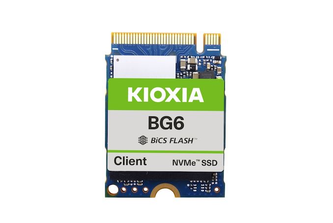
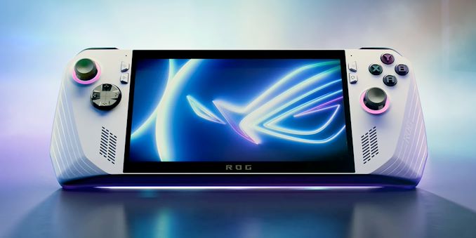
In the latest move in the tit-for-tat technology trade war between the United States and China, on Sunday the Cyberspace Administration of China announced that it was effectively banning Micron’s products from being purchased in the country going forward. Citing that Micron’s products have failed to pass its cybersecurity review requirements, the administration has ordered that operators of key infrastructure should stop buying products containing chips from the U.S.-based company.


“The review found that Meiguang’s products have serious hidden dangers of network security problems, which cause major security risks to China’s key information infrastructure supply chain and affect China’s national security,” a statement by CAC reads. “Therefore, the Cyber Security Review Office has made a conclusion that it will not pass the network security review in accordance with the law. According to the Cyber Security Law and other laws and regulations, operators of key information infrastructure in China should stop purchasing Micron’s products.”


The CAC statement does not elaborate on the nature of ‘hidden dangers’ and about the risks they pose. Furthermore, the agency did not detail which companies are considered as ‘operators of key information infrastructure,’ though we can speculate that these are telecommunication companies, government agencies, cloud datacenters serving socially important clients, and a variety of other entities that may deem crucial for the society or industries.


For U.S.-based Micron, while the Chinese market is a minor one overall, it’s not so small to be inconsequential. China and Hong Kong represent some 25% of Micron’s revenues, so the drop in sales is expected to have an impact on Micron’s financials.


“As we have disclosed in our filings, China and Hong Kong headquartered companies represent about 16% of our revenues,” said Mark Murphy, Chief Financial Officer at Micron, at the 51st Annual J.P. Morgan Global Technology, Media and Communications Conference. “In addition, we have distributors that sell to China headquartered companies. We estimate that the combined direct sales and indirect sales through distributors to China headquartered companies is about a quarter of our total revenue.”


The trade war implications aside, the ‘key information infrastructure’ wording of the government order leaves unclear for now on just how wide the Micron ban will be. Particularly, whether Micron’s products will still be allowed to be imported for rank-and-file consumer goods. Many of Micron’s Chinese clients assemble PCs, smartphones, and other consumer electronics sold all around the world, so the potential the impact on Micron’s sales could be significantly lower than 25% of its revenue so long as they are allowed to continue using Micron’s parts.


“We are evaluating what portion of our sales could be impacted by a critical information infrastructure ban,” Murphy added. “We are currently estimating a range of impact in the low single digits percent of our company total revenue at the low end and high single-digit percentage of total company revenue at the high end.”


The decision CAC decision comes after the U.S. government barred Chinese chipmakers from buying advanced wafer fab equipment, which is going to have a significant impact on China-based SMIC and YMTC, and years after the U.S. government implemented curbs that essentially drove one of China’s emerging DRAM makers out of business. Officially, whether or not the CAC decision has been influenced by the sanctions against Chinese companies by the U.S. government is an unanswered question, but as the latest barb between the two countries amidst their ongoing trade war, it’s certainly not unprecedented.


Sources: MicronReutersSeekingAlpha, CAC.


Source: AnandTech – Micron Expects Impact as China Bans Its Products from ‘Critical’ Industries

Intel HPC Updates For ISC 2023: Aurora Nearly Done, More Falcon Shores, and the Future of XPUs

With the annual ISC High Performance supercomputing conference kicking off this week, Intel is one of several vendors making announcements timed with the show. As the crown jewels of the company’s HPC product portfolio have launched in the last several months, the company doesn’t have any major new silicon announcements to make alongside this year’s show – and unfortunately Aurora isn’t yet up and running to take a shot at the Top 500 list. So, following a tumultuous year thus far that has seen significant shifts in Intel’s GPU roadmap in particular, the company is using ISC to recompose itself and use the backdrop of the show to lay out a fresh roadmap for HPC customers.


Most notably, Intel is using this opportunity to better explain some of the hardware development decisions the company has made this year. That includes Intel’s pivot on Falcon Shores, transforming it from XPU into a pure GPU design, as well to a few more high-level details of what will eventually become Intel’s next HPC-class GPU. Although Intel would clearly be perfectly happy to keep selling CPUs, the company has (and continues to) realign for a diversified market where their high-performance customers need more than just CPUs.


Source: AnandTech – Intel HPC Updates For ISC 2023: Aurora Nearly Done, More Falcon Shores, and the Future of XPUs

Kioxia BG6 Series M.2 2230 PCIe 4.0 SSD Lineup Adds BiCS6 to the Mix

Kioxia’s BG series of M.2 2230 client NVMe SSDs has proved popular among OEMs and commercial system builders due to their low cost and small physical footprint. Today, the company is introducing a new generation of products in this postage stamp-sized lineup. The BG6 series builds up on the Gen 4 support added in the BG5 by updating the NAND generation from BiCS5 (112L) to BiCS6 (162L) for select capacities. The increase in per-die capacity now allows Kioxia to bring 2TB M.2 2230 SSDs into the market. While the BG5 series came in capacities of up to 1TB, the BG6 series adds a 2TB SKU. However, the NAND generation update is only reserved for the 1TB and 2TB models.


The BG series of SSDs from Kioxia originally started out as a single-chip solution for OEMs either in a BGA package or a M.2 2230 module. The appearance of PCIe 4.0 and its demands for increased thermal headroom resulted in Kioxia getting rid of the single-chip BGA solution starting with the BG5 introduced in late 2021. The BG6 series continues the DRAMless strategy and dual-chip design (separate controller and flash packages) of the BG5.


While the performance numbers for the BG5 strictly placed it in the entry-level category for PCIe 4.0 SSDs, the update to the NAND has now amplified the performance to accepted mainstream levels for this segment. The DRAMless nature and use of the system DRAM (host memory buffer – HMB) for storing the flash translation layer (FTL) handicaps the performance slightly, preventing it from reaching high-end specifications. However, this translates to lower upfront cost and better thermal performance / lowered cooling costs – which are key constraints for OEMs and pre-built system integrators.


Kioxia BG6 SSD Specifications
Capacity 256 GB 512 GB 1 TB 2 TB
Form Factor M.2 2230 or M.2 2280
Interface PCIe Gen4 x4, NVMe 1.4c
NAND Flash 112L BiCS5 3D TLC 162L BiCS6 3D TLC
Sequential Read ? MB/s ? MB/s 6000 MB/s 6000 MB/s
Sequential Write ? MB/s ? MB/s 5000 MB/s 5300 MB/s
Random Read ? IOPS ? IOPS 650K IOPS 850K IOPS
Random Write ? IOPS ? IOPS 900K IOPS 900K IOPS
Power Active ? W ? W ? W ? W
Idle ? mW ? mW ? mW ? mW


The company is focusing on the 1TB and 2TB SKUs with BG6 due to higher demand for those capacities in the end market. The 256GB and 512GB variants are under development. While the M.2 2230 form-factor is expected to be the mainstay, Kioxia is also planning to sell single-sided M.2 2280 versions for systems that do not support M.2 2230 SSDs.


In addition to client systems, Kioxia also expects the BG6 SSDs to be used as boot drives in servers and storage arrays. Towards this, a few features that are not considered essential for consumer SSDs (such as support for NVMe 1.4c specifications including interfacing over SMBus for tigher thermal management, encryption using TCG Pyrite / Opal, power loss notification for protection against forced shutdowns, and platform firmware recovery) are included.


The availability of performance numbers for the 1TB SKU allows us to note that the BG6 has more than 1.7x the sequential performance numbers of the BG5, and random reads are 1.3x better, while random write performance has doubled. These are obviously fresh out-of-the-box numbers (as typical of specifications for consumer / client SSDs). Power consumption numbers were not made available at the time of announcement.


Kioxia will be sampling the drives to OEMs and system integrators in the second half of the year. Systems equipped with these drives can be expected in the hands of consumers for the holiday season or early next year. Pricing information was not provided as part of the announcement, but Kioxia is demonstrating these at the Dell Technologies World 2023 being held in Las Vegas from May 22 – 25.


Source: AnandTech – Kioxia BG6 Series M.2 2230 PCIe 4.0 SSD Lineup Adds BiCS6 to the Mix

Micron to Bring EUV to Japan: 1γ Process DRAM to Be Made in Hiroshima in 2025

Micron this week officially said that it would equip its fab in Hiroshima, Japan, to produce DRAM chips on its 1γ (1-gamma) process technology, its first node to use extreme ultraviolet lithography, in 2025. The company will be the first chipmaker to use EUV for volume production in Japan and its fabs in Hiroshima and Taiwan will be its first sites to use the upcoming 1γ technology.


As the only major DRAM maker that has not adopted extreme ultraviolet lithography, Micron planned to start using it with its 1γ process (its 3rd Generation 10nm-class node) in 2024. But due to PC market slump and its spending cuts, the company had to delay the plan to 2025. Micron’s 1γ process technology is set to use EUV for several layers, though it does not disclose how many layers will use it. 


What the company does say is that its 1γ node will enable the world’s smallest memory cell, which is bold claim considering the fact that Micron cannot possibly know what its rivals are going to have in 2025.


Last year the 1-gamma technology was at the ‘yield enablement’ stage, which means that the company was testing samples of DRAMs extensive testing and quality control procedures. At this point, the company may implement innovative inspection to tools to identify defects and then introduce certain improvements to certain process steps (e.g., lithography, etching) to maximize yields.


“Micron’s Hiroshima operations have been central to the development and production of several industry-leading technologies for memory over the past decade,” Micron President and CEO Sanjay Mehrotra said. “We are proud to be the first to use EUV in Japan and to be developing and manufacturing 1-gamma at our Hiroshima fab.


To produce memory chips on its 1-gamma node at its Hiroshima fab, Micron needs to install ASML’s Twinscan NXE scanners, which cost about $200 million per unit. To equip its fab with advanced tools, Micron secured ¥46.5 billion ($320 million) grant from the Japanese government last September. Meanwhile, Micron says it will invest ¥500 billion ($3.618 billion) in the technology ‘over the next few years, with close support from the Japanese government.’


“Micron is the only company that manufactures DRAM in Japan and is critical to setting the pace for not only the global DRAM industry but our developing semiconductor ecosystem,” said Satoshi Nohara, METI Director-General of the Commerce and Information Policy Bureau. “We are pleased to see our collaboration with Micron take root in Hiroshima with state-of-the-art EUV to be introduced on Japanese soil. This will not only deepen and advance the talent and infrastructure of our semiconductor ecosystem, it will also unlock exponential growth and opportunity for our digital economy.”


Source: AnandTech – Micron to Bring EUV to Japan: 1γ Process DRAM to Be Made in Hiroshima in 2025

Samsung Kicks Off DDR5 DRAM Production on 12nm Process Tech, DDR5-7200 in the Works

Samsung on Thursday said it had started high volume production DRAM chips on its latest 12nm fabrication process. The new manufacturing node has allowed Samsung to reduce the power consumption of its DRAM devices, as well as decrease their costs significantly compared to its previous-generation node.


According to Samsung’s announcement, the company’s 12nm fabrication process is being used to produce 16Gbit DDR5 memory chips. And while the company is already producing DDR5 chips with that capacity (e.g. K4RAH086VB-BCQK), the switch to the newer and smaller 12nm process has paid off both in terms of power consumption and die size. As compared to DDR5 dies made on the company’s previous-generation node (14nm), the new 12nm dies offer up to 23% lower power consumption, and Samsung is able to produce 20% more dies per wafer (i.e., the DDR5 dies are tangibly smaller). 


Samsung says that the key innovation of its 12nm DRAM fabrication process is usage of new high-k material for DRAM cell capacitors that enabled it to increase cell’s capacitance to boost performance, but without increasing their dimensions and die sizes. Higher DRAM cell capacitance means a DRAM cell can store more data and reduce power-draining refresh cycles, hence increasing performance. However, larger capacitors typically result in increased cell and die size, which makes the resulting dies more expensive.


DRAM makers have been addressing this by using high-k materials for years, but finding these materials is getting trickier with each new node as memory makers also have to take into account yields and production infrastructure they have. Apparently, Samsung has succeeded in doing so with its 12nm node, though it does not make any disclosures on the matter. That Samsung has succeeded in reducing their die size by a meaningful amount at all is quite remarkable, as analog components like capacitors were some of the first parts of chips to stop scaling down further with finer process nodes.


In addition to introducing a new high-k material, Samsung also reduced operating voltage and noise for its 12nm DDR5 ICs to offer a better balance of performance and power consumption compared to predecessors.


One of the aspects about Samsung’s 12nm DRAM technology is that it looks to be the company’s 3rd Generation production node for memory that uses extreme ultraviolet lithography. The first D1x node was purely designed as a proof of concept and its successor D1a, which has been in use since 2021, used EUV for five layers. Meanwhile, it is unclear to what degree Samsung’s 12nm node is using EUV tools.


“Using differentiated process technology, Samsung’s industry-leading 12nm-class DDR5 DRAM delivers outstanding performance and power efficiency,” said Jooyoung Lee, Executive Vice President of DRAM Product & Technology at Samsung Electronics. 


Meanwhile, Samsung is also eyeing faster memory speeds with their new 12nm DDR5 dies. According to the company, these dies can run as fast as DDR5-7200 (i.e. 7.2Gbps/pin), which is well ahead of what the official JEDEC specification currently allows for. The voltage required isn’t being stated, but if nothing else, it offers some promise for future XMP/EXPO memory kits.


Source: AnandTech – Samsung Kicks Off DDR5 DRAM Production on 12nm Process Tech, DDR5-7200 in the Works

Voltage Lockdown: Investigating AMD's Recent AM5 AGESA Updates on ASRock's X670E Taichi

It’s safe to say that the last couple of weeks have been a bit chaotic for AMD and its motherboard partners. Unfortunately, it’s been even more chaotic for some users with AMD’s Ryzen 7000X3D processors. There have been several reports of Ryzen 7000 processors burning up in motherboards, and in some cases, burning out the chip socket itself and taking the motherboard with it.


Over the past few weeks, we’ve covered the issue as it’s unfolded, with AMD releasing two official statements and motherboard vendors scrambling to ensure their users have been updating firmware in what feels like a grab-it-quick fire sale, pun very much intended. Not everything has been going according to plan, with AMD having released two new AGESA firmware updates through its motherboard partners to try and address the issues within a week.


The first firmware update made available to vendors, AGESA 1.0.0.6, addressed reports of SoC voltages being too high. This AGESA version put restrictions in place to limit that voltage to 1.30 V, and was quickly distributed to all of AMD’s partners. More recently, motherboard vendors have pushed out even newer BIOSes which include AMD’s AGESA 1.0.0.7 (BETA) update. With even more safety-related changes made under the hood, this is the firmware update AMD and their motherboard partners are pushing consumers to install to alleviate the issues – and prevent new ones from occurring.


In this article, we’ll be taking a look at the effects of all three sets of firmware (AGESA 1.0.0.5c – 7) running on our ASRock X670E Taichi motherboard. The goal is to uncover what, if any, changes there are to variables using the AMD Ryzen 9 7950X3D, including SoC voltages and current drawn under intensive memory based workloads.


Source: AnandTech – Voltage Lockdown: Investigating AMD’s Recent AM5 AGESA Updates on ASRock’s X670E Taichi

Solidigm D5-P5430 Addresses QLC Endurance in Data Center SSDs

Solidigm has been extremely bullish on QLC SSDs in the data center. Compared to other flash vendors, their continued use of a floating gate cell architecture (while others moved on to charge trap configurations) has served them well in bringing QLC SSDs to the enterprise market. The company realized early on that the market was hungry for a low-cost high-capacity SSD to drive per-rack capacity. In order to address this using their 144L 3D NAND generation, Solidigm created the D5-P5316. While the lineup did include a 30TB SKU for less than $100/TB, the QLC characteristics in general, and the use of a 16KB indirection unit (IU) resulted in limiting the use-cases to read-heavy and large-sized sequential / random write workloads.


Solidigm markets their data center SSDs under two families – the D7 line is meant for demanding workloads with 3D TLC flash. The D5 series, on the other hand, uses QLC flash and targets mainstream workloads and specialized non-demanding use-cases where density and cost are more important. The company further segments this family into the ‘Essential Endurance’ and ‘Value Endurance’ line. The popular D5-P5316 falls under the ‘Value Endurance’ line.


The D5-P5430 being introduced today is a direct TLC replacement drive in the ‘Essential Endurance’ line. This means that, unlike the D5-P5316’s 16K IU, the D5-P5430 uses a 4KB IU. The company had provided an inkling of this drive in their Tech Field Day presentation last year.


Despite being a QLC SSD, Solidigm is promising very competitive read performance and higher endurance ratings compared to previous generation TLC drives from its competitors. In fact, Solidigm believes that the D5-P5430 can be quite competitive against TLC drives like the Micron 7450 Pro and Kioxia CD6-R.


Solidigm D5-P5430 NVMe SSD Specifications
Aspect Solidigm D5-P5430
Form Factor 2.5″ 15mm U.2 / E3.S / E1.S
Interface, Protocol PCIe 4.0 x4 NVMe 1.4c
Capacities 3.84 TB, 7.68 TB, 15.36 TB

E1.S / U.2 / E3.S
30.72 TB

U.2 / E3.S
3D NAND Flash Solidigm 192L 3D QLC
Sequential Performance (GB/s) 128KB Reads @ QD 256 7.0
128KB Writes @ QD 256 3.0
Random Access (IOPS) 4KB Reads @ QD 256 971K
4KB Writes @ QD 256 120K
Latency (Typical) (us) 4KB Reads @ QD 1 108
4KB Writes @ QD 1 13
Power Draw (Watts) 128KB Sequential Read ??
128KB Sequential Write 25.0
4KB Random Read ??
4KB Random Write ??
Idle 5.0
Endurance (DWPD) 100% 128KB Sequential Writes 1.83
100% 4KB Random Write 0.58
Warranty 5 years


Based on market positioning, the Micron 6500 ION launched earlier today is the main competition for the D5-P5430. The sequential writes and power consumption numbers are not particularly attractive for the Solidigm drive on a comparative basis, but the D5-P5430 does win out on the endurance aspect – 0.3 RDWPD for the 6500 ION against 0.58 RDWPD for the D5-P5430 (surprising for a QLC drive). Solidigm prefers total NAND writes limit as a better estimtate of endurance and quotes 32 PBW as the endurance rating for the D5-P5430’s maximum capacity SKU. Another key aspect here is that the D5-P5430 is only available in capacities up to 15.36 TB today. The 30 TB SKU is slated to appear later this year. In comparison, the 30 TB SKU for the 6500 ION is available now. On the other hand, the D5-P5430 is available in a range of capacities and form-factors, unlike the 6500 ION. The choice might just end up being dependent on how each SSD performs for the intended use-cases.


Source: AnandTech – Solidigm D5-P5430 Addresses QLC Endurance in Data Center SSDs

Micron Updates Data Center NVMe SSD Lineup: 6500 ION TLC and XTR SLC

Micron is expanding its data center SSD lineup today with the introduction of two new products – the 6500 ION and the XTR NVMe SSDs. These two products do not fall into any of their existing enterprise SSD lineups. They are meant to fill holes in their product stack for high-capacity and high-endurance offerings. While the Micron 6500 ION is a TLC drive with QLC pricing, the XTR NVMe SSD is a SLC offering. Read on for a closer look at the specifications and market positioning of the two products.


Source: AnandTech – Micron Updates Data Center NVMe SSD Lineup: 6500 ION TLC and XTR SLC

Asus Formally Unveils ROG Ally Portable Console: Eight Zen 4 Cores and RDNA 3 GPU in Your Hands

Asus on Thursday officially introduced the ROG Ally, its first handheld gaming PC. With numerous handheld gaming systems around, most notably Steam Deck, Asus needed something special to be successful and fulfill the promise of the ROG brand. To that end, the ROG Ally promises a unique combination of performance enabled by AMD’s latest mobile CPU, high compatibility due to usage of Windows 11, portability, and other features.


Performance: To Extreme, or Not to Extreme?


First teased by Asus last month, the ROG Ally is the company’s effort to break into the handheld gaming PC space, which Valve has essentially broken open in the past year with the Steam Deck.


When developing ROG Ally, Asus wanted to build a no-compromise machine that would bring the performance of mobile PCs the portability that comes with handheld device. This is where AMD’s recently-launched Zen 4-based Ryzen Z1 and Ryzen Z1 Extreme SoCs, which are aimed specifically at ultra-portable devices, come into play.


Based on AMD’s 4nm Phoenix silicon, the eight-core Ryzen Z1 Extreme processor and its 12 CU RDNA 3-based GPU resembles the company’s Ryzen 7 7840U CPU. Meanwhile Asus is also offering a version of Ally using the lower-tier Z1 chip, which still uses eight CPU cores and pairs that with a 4 CU GPU. On paper, the Z1 Extreme chip is significantly more powerful in graphics tasks as a result (~3x), however in practice the chips are closer, as thermal and memory bandwidth limits keep the Extreme chip from running too far ahead.


Speaking of graphics performance, it should be noted that Asus’s ROG Ally console is equipped with the ROG XG Mobile connector (a PCIe 3.0 x8 for data and a USB-C for power and USB connections) that can be used to connect an Asus ROG XG Mobile eGFX dock with the handheld. The XG docks come with a range of GPUs installed, up to a GeForce RTX 4090 Laptop GPU. The XG dock essentially transforms ROG Ally into a high-performance gaming system, albeit by supplanting much of its on-board functionality. The fact that Asus offers eGFX capability right out-of-box is a significant feature differentiator for the ROG Ally, though be prepared to invest the $1999.99 if you want the top-end GeForce RTX 4090 Laptop-equipped XG dock.


Both versions of ROG Ally will come with 16GB of LPDDR5-6400 memory and a 512GB SSD in an M.2-2230 form-factor with a PCIe 4.0 interface. While replacing the M.2 drive is reportedly a relatively easy task, for those who want to expand storage space without opening anything up, the console also has an UHS-II-compliant microSD card slot.


Display: Full-HD at 120 Hz


The ROG Ally is not only the first handheld with the Ryzen Z1 Extreme CPU, but will also be among the first portable game consoles with a 1920×1080 resolution 7-inch display; and one that supports a maximum refresh rate of 120 Hz, no less. The Gorilla Glass Victus-covered display uses an IPS-class panel with a peak luminance of 500 nits as well as Dolby Vision HDR support to make games more appealing.


In addition to Dolby Vision HDR-badged display, the Asus ROG Ally also has Dolby Atmos-certified audio subsystem with Smart Amp speakers and noise cancelation technology. 


Ergonomics: 600 Grams and All the Controls


When it comes to mobile devices, ergonomics is crucial. Yet, it is pretty hard to design a handheld game console that essentially uses laptop-class silicon with all of its peculiarities. When Asus began work on its ROG Ally, it asked mobile gamers about what they think was the most important feature for their portable console and apparently it was weight. So Asus set about deigning a device that would weigh around 600 grams and would be comfortable to use.


“When we go through survey with our focus group, the number one thing that they wanted was a balanced weight handheld device,” said Shawn Yen, vice president of Asus’s Gaming Business Unit responsible for ROG products. “The target was 600 grams because the current handheld devices in the market today are too heavy. It is not something that they can engage for a very long period of time. So, their game time got cut down because it is not comfortable. So, uh, when we first thought about the design target for ROG Ally, we were thinking about a device that can get into gamers’ hands for hours of fun time.”


The display and chassis are among the heaviest components of virtually all mobile devices, so there is little that can be done about those. But in a bid to optimize the weight and distribute it across the device, the company had to implement a very well thought motherboard design, and use anti-gravity heat pipes to ensure proper cooling at all times without using too many of them as this increases weight. Meanwhile, Asus still had to use two fans and a radiator with 0.1 mm ultra-thin fins to ensure that the CPU is cooled down properly as it still can dissipate up to 30W of heat. To further optimize weight, Asus opted for a polycarbonate chassis.


Since Asus ROG Ally is essentially a Windows 11-based PC albeit in a portable game console form factor, the company had to incorporate all the pads and buttons featured on conventional gamepads and some more controls for Windows (e.g., touchscreen) and ROG Ally-specific things like Armor Crate game launcher and two macro buttons. It’s also worth noting that, seemingly because of the use of Windows 11, the Ally is not capable of consistently suspending games while it sleeps, a notable difference compared to other handheld consoles.


Meanwhile, the trade-off to hitting their weight target while still using a relatively powerful SoC has been battery life. The Ally comes with a 40Wh batter, and Asus officially advertises the handheld as offering up to 2 hours of battery life in heavy gaming workloads. Early reviews, in turn, have matched this, if not coming in below 2 hours in some cases. The higher-resolution display and high-performance AMD CPU are both key differentiating factors of the Ally, but these parts come at a high power cost.


Vast Connectivity


Being a PC, the ROG Ally is poised to offer connectivity that one comes to expect from a portable computer. Therefore, the unit features a Wi-Fi 6E and Bluetooth adapter for connectivity, it includes a MicroSD card slot for additional storage, a USB Type-C port for both charging and display output, an ROG XG Mobile connector for external GPUs, and a TRRS audio connector for headsets.


The Price


The ROG Ally with AMD’s Ryzen Z1 Extreme CPU is set to be launched globally on June 13, 2023, at a price point of $699.99. Meanwhile the non-extreme Z1 version of the Ally has been lited for $599.99, though no release date has been set. The first reviews are already out, so Asus is giving potential customers a long lead time to evaluate the console before it’s released next month.


Source: AnandTech – Asus Formally Unveils ROG Ally Portable Console: Eight Zen 4 Cores and RDNA 3 GPU in Your Hands

Asus Unveils Two Slimmer GeForce RTX 4090 Video Cards: ROG Strix LC and TUF OG

Asus has expanded the company’s GeForce RTX 40-series product portfolio with two new RTX 4090 graphics cards. The ROG Strix LC GeForce RTX 4090 and TUF Gaming GeForce RTX 4090 OC, which are available in regular and OC editions, have arrived to compete in the high-end segment. What makes these cards notable, in turn, is their reduced size: the new cards are physically smaller than Asus’ early RTX 4090 offerings, as well as many of the competitors on the market.


The GeForce RTX 4090 is a 450W gaming graphics card, with large coolers to match. Even NVIDIA’s hard-to-get GeForce RTX 4090 Founders Edition is a triple-slot graphics card, and air-cooled AIB cards tend to be larger still. So for the size-conscious gamer, this leaves liquid cooled cards, which brings us to Asus’s new ROG Strix LC GeForce RTX 4090. The closed-loop card moves a lot of its bulk off to an attached 240 mm radiator block, bringing the card itself down to 2.6-slots wide.


The ROG Strix LC GeForce RTX 4090’s hybrid cooling system packs a cold plate that cools the large AD102 GPU and neighboring GDDR6X memory chips. The heat is transferred to the 240 mm radiator through 560 mm tubing, so there won’t be an issue with large cases. A low-profile heatsink with a blower-style cooling fan keeps the other power delivery components cool. Meanwhile the radiator itself is equipped with a pair of 120 mm ARGB cooling fans are present to dissipate the heat once it gets there.


Asus GeForce RTX 4090 Specifications
AnandTech ROG Strix LC GeForce RTX 4090 TUF Gaming GeForce RTX 4090 OG TUF Gaming GeForce RTX 4090
Regular Edition Boost Clock

(Default / OC)
2,520 MHz / 2,550 MHz 2,520 MHz / 2,550 MHz 2,520 MHz / 2,550 MHz 
OC Edition

Boost Clock

(Default / OC)
2,610 MHz / 2,640 MHz 2,565 MHz / 2,595 MHz  2,565 MHz / 2,595 MHz
Display Outputs 2 x HDMI 2.1a

3 x DisplayPort 1.4a
2 x HDMI 2.1a

3 x DisplayPort 1.4a
2 x HDMI 2.1a

3 x DisplayPort 1.4a
Design 2.6 Slot 3.2 Slot 3.65 Slot
Power Connectors 1 x 16-pin 1 x 16-pin 1 x 16-pin
Dimensions 293 x 133 x 52 mm

 
325.9 x 140.2 x 62.8 mm 348.2 x 150 x 72.6 mm
Radiator Dimensions 272 x 121 x 54 mm N/A N/A


Asus’s other new RTX 4090 card, the air-cooled TUF Gaming GeForce RTX 4090 OG, is a unique case of its own. Technically, it’s a new SKU; however, the graphics card reuses the TUF Gaming cooler from the TUF Gaming GeForce RTX 3090 Ti.


This is notable because the TUF cooler used on the 3090 Ti was a good bit smaller than Asus’s first RTX 4090 cooler. The net result is that these changes bring the new OG card’s width from 3.65-slots (and arguably, wide enough that you need to leave a 4th slot open for air flow) down to 3.2 slots – just enough room for proper airflow if the neighboring 4th sot is occupied. Altogether, the OG model is smaller in every dimension, shaving off 6% of its height, 7% of its length, and 13% of its width. Asus doesn’t list the weight of its graphics cards, so we cannot comment on whether the new OG version has lost weight.


By most accounts, Asus’s current RTX 4090 cooler is highly effective – it’s just also really big. So offering a separate SKU with a smaller cooler makes a good deal of sense, especially given how popular NVIDIA’s true triple-slot Founders Edition card has been. The smaller TUF cooler is rated for the same 450W TDP as the larger TUF 4090 cooler, but, as always, there may be performance/acoustic tradeoffs involved.


There’s one other change that Asus doesn’t advertise with the TUF Gaming GeForce RTX 4090 OG. The renders on the product page show the graphics card with a longer PCB. One of the advantages of the more compact PCB on the previous model was that it permitted Asus (and NVIDIA) to vent heat out of the back side of the card, as well as to optimize the trace layouts and component placement. Meanwhile, with the longer PCB, Asus relocated the 16-pin power connector. Instead of being placed in the middle, the power connector is on the farther right side.


Between the two new cards, the ROG Strix LC GeForce RTX 4090 ends up with the edge in clockspeeds, flaunting boost clock speeds up to 2,640 MHz when in its highest performance mode. Meanwhile, the TUF Gaming GeForce RTX 4090 OG series have the same clock speeds as the vanilla models, with a rated boost clock of 2520 MHz stock and 2595 MHz when the OC card is in its highest mode. In addition, the ROG Strix LC GeForce RTX 4090 and TUF Gaming GeForce RTX 4090 OG have other attributes in common, including using a single 16-pin power connector and a display output layout consisting of two HDMI 2.1a ports and three DisplayPort 1.4a outputs.


Asus hasn’t revealed the pricing or availability of the new graphics cards. For reference, the TUF Gaming GeForce RTX 4090 and OC Edition retail for $1,599 and $1,799, respectively. The OG counterparts likely have similar price tags. Meanwhile, we’d expect the ROG Strix LC GeForce RTX 4090 to carry a more considerable premium due to the AIO liquid cooling design.


Source: AnandTech – Asus Unveils Two Slimmer GeForce RTX 4090 Video Cards: ROG Strix LC and TUF OG

Philips Reveals Dual Screen Display: a 24-Inch LCD with E Ink Secondary Screen

Although E Ink technology has remained a largely niche display tech over the past decade, it’s none the less excelled in that role. The electrophoretic technology closely approximates paper, providing significant power advantages versus traditional emissive displays, not to mention making it significantly easier on readers’ eyes in some cases. And while the limitations of the technology make it unsuitable for use as a primary desktop display, Phillips thinks there’s still a market for it as a secondary display. To that end, Philips this week has introduced their novel, business-oriented Dual Screen Display, which combines both an LCD panel and and E Ink panel into a single display, with the aim of capturing the benefits of both technologies.


The Philips Dual Screen Display (24B1D5600/96) is a single display that integrates both a 23.8-inch 2560×1440 IPS panel as well as a 13.3-inch, greyscale 1200×1600 resolution E Ink display. With each display operating independently, the idea is similar to previous concepts of multi-panel monitors; however Phillips is taking things in a different direction by using an E Ink display as a second panel – combining two otherwise very different display technologies into a single product. By offering an E Ink panel in this product, Phillips is looking to court the market for users who would prefer the reduced eye strain of an E Ink display, but are working at a desktop computer, where an E Ink display would not be viable as a primary monitor.


As you might expect from the basic layout of the monitor, the primary panel is a rather typical office display that’s designed for video and productivity applications – essentially anything where you need a modern, full color LCD. The secondary E Ink display, on the other hand, is a greyscale screen whose strength is the lack of flicker that comes from not being backlit by a PWM light. Both screens act independently, but since they are encased into the same chassis, they are meant to work together. For example, the secondary monitor can display supplementary information in text form, whereas the primary monitor can display photos.


Ultimately, Philips is pitching the display on the idea that the secondary screen can reduce the eye strain of the viewer while viewing documents. It’s a simple enough concept, but one that requires buyers to overlook the trade-offs of E Ink, and the potential drawbacks of having two dissimilar displays directly next to each other.


Under the hood, the LCD panel on the Deal Screen Display is an unremarkable office-grade display. Phillips is using 23.8-inch anti-glare 6-bit + Hi FRC IPS panel with a 2560×1440 resolution, which can hit a maximum brightness of 250 nits while delivering 178-degree viewing angles. Meanwhile, the E Ink panel is a 13.3-inch 4-bit greyscale electrophoretic panel, with a resolution of 1200×1600. Notably here, there is no backlighting; the E Ink panel is meant to be environmentally lit (e.g. office lighting) to truly minimize eye strain.


When it comes to connectivity, the primary screen is equipped with a DisplayPort 1.2 and a USB Type-C input (with DP Alt mode and USB Power Delivery support), a USB hub, and a GbE adapter. Meanwhile, the secondary screen connects to host using a USB Type-C connector that also supports DP Alt Mode, and Power Delivery.


Specifications of the Philips Dual Screen Display

24B1D5600/96
  Primary Screen Secondary Screen
Panel 27″ IPS 6-bit + Hi FRC 13.3″ E Ink 4-bit
Native Resolution 2560 × 1440 1200 × 1600
Maximum Refresh Rate 75 Hz ?
Response Time 4ms ?
Brightness 250 cd/m² (typical) ?
Contrast 1000:1 ?
Viewing Angles 178°/178° horizontal/vertical high
HDR none none
Dynamic Refresh Rate none none
Pixel Pitch 0.2058 mm² 0.2058 mm²
Pixel Density 123 ppi 150 ppi
Display Colors 16.7 million greyscale
Color Gamut Support NTSC: 99%

sRGB: 99%
4-bit
Aspect Ratio 16:9 3:4
Stand Height: +/-100 mm

Tilt: -5°/23°

Swivel: 45°
Inputs 1 × DisplayPort (HDCP 1.4)

1 × USB-C (HDCP 1.2 + PD)
1 × USB-C (HDCP 1.4 + PD)
Outputs
USB Hub USB 3.0 hub
Launch Date Q2 2023


The Philips Dual Screen Display has a rather sleek stand which can adjust height, tilt, and swivel. It makes the whole unit look like one monitor rather than like two separate screens. Though to be sure, the E Ink portion of the display can be angled independently from the LCD panel, allowing the fairly wide monitor to contour to a user’s field of view a bit better.


When it comes to pricing, Philips’s Dual Screen Display is available in China for $850 (according to Liliputing), which looks quite expensive for a 24-inch IPS LCD and a 13.3-inch secondary screen. Though as this is a rather unique product, it is not surprising that it is sold at a premium.


Source: AnandTech – Philips Reveals Dual Screen Display: a 24-Inch LCD with E Ink Secondary Screen

Samsung to Unveil Refined 3nm and Performance-Enhanced 4nm Nodes at VLSI Symposium

Samsung Foundry is set to detail its second generation 3 nm-class fabrication technology as well as its performance-enhanced 4 nm-class manufacturing process at the upcoming upcoming 2023 Symposium on VLSI Technology and Circuits in Kyoto, Japan. Both technologies are important for the contract maker of chips as SF3 (3GAP) promises to offer tangible improvements for mobile and SoCs, whereas SF4X (N4HPC) is designed specifically for the most demanding high-performance computing (HPC) applications.


2nd Generation 3 nm Node with GAA Transistors


Samsung’s upcoming SF3 (3GAP) process technology is an enhanced version of the company’s SF3E (3GAE) fabrication process, and relies on its second-generation gate-all-around transistors – which the company calls Multi-Bridge-Channel field-effect transistors (MBCFETs). The node promises additional process optimizations, though the foundry prefers not to compare SF3 with SF3E. Compared to its direct predecessor, SF4 (4LPP, 4nm-class, low power plus), SF3 claims a 22% performance boost at the same power and complexity or a 34% power reduction at the same clocks and transistor count, as well as a 21% logic area reduction. Though it is unclear whether the company has achieved any scaling for SRAM and analogue circuits.


In addition, Samsung claims that SF3 will provide additional design flexibility facilitated by varying nanosheet (NS) channel widths of the MBCFET device within the same cell type. Curiously, variable channel width is a feature of GAA transistors that has been discussed for years, so the way Samsung is phrasing it in context of SF3 might mean that SF3E does not support it.


Thus far neither Samsung LSI, the conglomerate’s chip development arm, nor other customers of Samsung Foundry have formally introduced a single highly-complex processor mass produced on SF3E/3GAE process technology. In fact, it looks like the only publicly-acknowledged application that uses the industry’s first 3 nm-class fabrication process is a cryptocurrency mining chip, according to TrendForce. This is not particularly surprising as usage of Samsung’s ‘early’ nodes is typically quite limited. 


By contrast, Samsung’s ‘plus’ technologies are typically used by a wide range of customers, so the company’s SF3 (3GAP) process is likely to see much higher volumes when it becomes available sometime in 2024.


SF4X for Ultra-High-Performance Applications


In addition to SF3, which is designed for a variety of possible use cases, Samsung Foundry is prepping its SF4X (4HPC, 4 nm-class high-performance computing) designed for performance-demanding applications like datacenter-oriented CPUs and GPUs.


To address such chips, Samsung’s SF4X offers a performance boost of 10% coupled with a 23% power reduction. Samsung doesn’t explicitly specify what process node that comparison is being made against, but presumably, this is against their default SF4 (4LPP) fabrication technology. To achieve this, Samsung redesigned transistors’ source and drain after reassessing their stresses (presumably under high loads), performed further transistor-level design-technology co-optimization (T-DTCO), and introduced a new middle-of-line (MOL) scheme. 


The new MOL enabled SF4X to offer a silicon-proven CPU minimum voltage (Vmin) of 60mV, a 10% decrease in the variation of off-state current (IDDQ), guaranteed high voltage (Vdd) operation at over 1V without performance degradation, and an improved SRAM process margin.


Samsung’s SF4X will be a rival for TSMC’s N4P and N4X nodes, which are due in 2024 and 2025 respectively. Based on claim specificaitons alone, it is hard to tell which technology will offer the best combination of performance, power, transistor density, efficiency, and cost. That said, SF4X will be Samsung’s first node in the recent years that was specifically architected with HPC in mind, which implies that Samsung has (or is expecting) enough customer demand to make it worth their time.


Source: AnandTech – Samsung to Unveil Refined 3nm and Performance-Enhanced 4nm Nodes at VLSI Symposium

NVIDIA Launches Diablo IV Bundle for GeForce RTX 40 Video Cards

NVIDIA is launching a new game bundle for its latest generaiton GeForce RTX 40-series graphics cards and OEM systems. This time, NVIDIA has teamed up with Activision Blizzard to offer a free copy of the latest iteration of their wildly popular action RPG series, Diablo IV.


This promotion will run globally, starting now and running through June 16, 2023. For more than a month, customers purchasing GeForce RTX 4090, 4080, 4070 Ti, 4070 graphics cards or desktops containing one of them from various vendors will get a free digital download code of Diablo IV Standard Edition on Battle.net. The code for the title must be redeemed before July 13, 2023.


NVIDIA Current Game Bundles

(May 2023)
Video Card

(incl. systems and OEMs)
Game
GeForce RTX 40 Series Desktop (All) Diablo IV
GeForce RTX 30 Series Desktop (All) None
GeForce RTX 40 Series Laptop (All) None
GeForce RTX 30 Series Laptop (All) None


For NVIDIA, Diablo IV will also be a technology showcase, as it is set to support the DLSS 3 upscaling technology as well as the Reflex latency cutting out-of-box at launch. Ray tracing is also slated to be added at some point after the game launches. At retail pricing, Activision Blizzard’s Diablo IV Standard Edition costs $69.99 at Battle.net, though NVIDIA is undoubtedly getting a bulk deal.


It should be noted that this latest game bundle is just for NVIDIA’s RTX 40 series desktop cards. Unlike the since-expired Redfall bundle, NVIDIA is not offering Diablo IV (or any other games) with GeForce-based laptops. Nor are any remaining GeForce RTX 30 series producted covered.


Diablo IV will officially release on June 4, 2023.


Source: NVIDIA


Source: AnandTech – NVIDIA Launches Diablo IV Bundle for GeForce RTX 40 Video Cards

AMD To Host AI and Data Center Event on June 13th – MI300 Details Inbound?

In a brief note posted to its investor relations portal this morning, AMD has announced that they will be holding a special AI and data center-centric event on June 13th. Dubbed the “AMD Data Center and AI Technology Premiere”, the live event is slated to be hosted by CEO Dr. Lisa Su, and will be focusing on AMD’s AI and data center product portfolios – with a particular spotlight on AMD’s expanded product portfolio and plans for growing out these market segments.


The very brief announcement doesn’t offer any further details on what content to expect. However, the very nature of the event points a clear arrow at AMD’s forthcoming Instinct Mi300 accelerator. MI300 is AMD’s first shot at building a true data center/HPC-class APU, combining the best of AMD’s CPU and GPU technologies. AMD has offered only a handful of technical details about MI300 thus far – we know it’s a disaggregated design, using multiple chiplets built on TSMC’s 5nm process, and using 3D die stacking to place them over a base die – and with MI300 slated to ship this year, AMD will need to fill in the blanks as the product gets closer to launch.


As we noted in last week’s AMD earnings report, AMD’s major investors have been waiting with baited breath for additional details on the accelerator. Simply put, investors are treating data center AI accelerators as the next major growth opportunity for high-performance silicon – eyeing the high margins these products have afforded over at NVIDIA and other AI-adjacent rivals – so there is a lot of pressure on AMD to claim a slice of what’s expected to be a highly profitable pie. MI300 is a product that has been in the works for years, so the pressure is more of a reaction to the money than the silicon itself, but still, MI300 is expected to be AMD’s best opportunity yet to capture a meaningful portion of the data center GPU market.


MI300 aside, given the dual AI and data center focus of the event, this is also where we’re likely to see more details on AMD’s forthcoming EPYC “Genoa-X” CPUs. The L3 V-Cache-equipped version of AMD’s current-generation EPYC 9004 series Genoa CPUs, Genoa-X has been on AMD’s roadmap for a while. And with their consumer equivalent parts already shipping (Ryzen 7000X3D), AMD should be nearing completion of the EPYC parts. AMD has previously confirmed that Genoa-X will ship with up to 96 CPU cores, with over 1GB in total L3 cache available on the chip to further boost performance on workloads that benefit from the extra cache.


AMD’s ultra-dense EPYC Bergamo chip is also in the pipeline, though given the high-performance aspects of the presentation, it’s a little more questionable whether it will be at the show. Based on AMD’s compacted Zen4c architecture, Bergamo is aimed at cloud service providers who need lots of cores to split up amongst customers, with up to 128 CPU cores on a single Bergamo chip. Like Genoa-X, Bergamo is slated to launch this year, so further details about it should come to light sooner than later.


But whatever AMD does (or doesn’t) show at their event, we’ll find out on June 13th at 10am PT (17:00 UTC). AMD will be live streaming the event from their website as well as YouTube.


Source: AnandTech – AMD To Host AI and Data Center Event on June 13th – MI300 Details Inbound?

Noctua Publishes Roadmap: Next-Gen AMD Threadripper Coolers Incoming

Unlike other makers of cooling systems, Noctua has its roadmap advertised on its websites and always updates it to reflect changes in its product development plans. The company’s May 2023 roadmap brings several surprises as it adds ‘Next-gen AMD Threadripper coolers’ and removes white fans from its plans.


The main thing that strikes the eye in Noctua’s roadmap is the mention of ‘next-gen AMD Threadripper coolers’ coming in the third quarter. These products were not on the roadmap in January, per a slide published by Tom’s Hardware. AMD has been rumored to introduce its next-generation Ryzen Threadripper processors for workstations for a while, but this is almost the first time when we have seen a more or less official confirmation about the existence of such plans, albeit not from AMD, but one of its partners. 


Since the confirmation does not come from the CPU developer, we would not put our money into launching the next-generation Ryzen Threadripper based on the Zen 4 microarchitecture in Q3. Meanwhile, it is reasonable to expect AMD’s codenamed Storm Peak processor to arrive sooner than later since the company has not updated this lineup in a while.


Other notable things in Noctua’s roadmap are a bunch of Chromax black products due in Q4, a 24V to 12V voltage converted set to arrive in Q2, and a 24V 40-mm fan, which emphasizes that the company considers the ATX12VO ecosystem essential to address. In addition, the firm is prepping its next-generation 140-mm fans, which will arrive in Q1 2024 in regular colors and then later in the year in Chromax—black version.


Unfortunately, Noctua’s next-generation NH-D15 cooler, which once was promised to arrive in Q1 2023, is not slated for sometime in 2024. Meanwhile, the company’s roadmap no longer includes white fans for a reason we cannot explain. Perhaps, the company decided to devote its resources elsewhere, or maybe white plastic that the company considered for white fans did not meet its expectations.


Source: Noctua


Source: AnandTech – Noctua Publishes Roadmap: Next-Gen AMD Threadripper Coolers Incoming

Samsung Foundry Vows to Surpass TSMC Within Five Years

The head of Samsung’s semiconductor unit acknowledged last week that the company’s current mass production, leading-edge process technologies are a couple of years behind TSMC’s most advanced production nodes. But Samsung is working hard to catch up with its larger rival in five years. 


“To be honest, Samsung Electronics’ foundry technology lags behind TSMC,” said Dr. Kye Hyun Kyung, the head of the Samsung Electronics Device Solutions Division, overseeing global operations of the Memory, System LSI and Foundry business units,” at a lecture at the Korea Advanced Institute of Science & Technology (KAIST), reports Hankyung. “We can outperform TSMC within five years.”


Samsung has been investing tens of billions of dollars in its foundry division in the recent years in a bid to catch up with TSMC and Intel, both in terms of production capacity for LSI chips as well as process technology advantages. The company has significantly closed the gap with its rivals, but it is still not quite on par with TSMC’s fabrication technologies when it comes to performance, power, area (transistor density), and cost metrics.


While Samsung Foundry is the first contract maker of chips to adopt gate-all-around (GAA) transistors with its SF3E (3GAE, 3 nm, gate-all-around early) node, and the company’s customers are enthusiastic about the technology itself and the novel transistor architecture, this process is not used for Samsung’s own leading-edge system-on-chips for smartphones. 


“Customers’ response to Samsung Electronics’ 3nm GAA process is good,” said Dr. Kye Hyun Kyung.


Meanwhile, Samsung’s latest Galaxy S23-series uses Qualcomm’s Snapdragon 8 Gen 2 SoC is made by TSMC on its N4 fabrication process.


Samsung Foundry’s most advanced technology that can be used to make highly-complex SoCs for smartphones or other demanding applications is SF4 (4LPP, 4 nm, low-power plus), which, as the company admits, is significantly behind TSMC’s N3 (N3B) node, is rumored to be used for mass production of Apple’s highly-complex SoCs at this time.


The company may somewhat close the gap with TSMC’s N3 and N4P with its SF4P (4LPP+) that will be available for customers later this year, according to a clarification published by @Tech_Reve.


Samsung Foundry will have a better chance to catch up with TSMC when its SF3 (3GAP) fabrication node enters high volume production in 2024, though by the time TSMC will also be offering its more advanced N3P manufacturing technology.  Around the same time Samsung also plans to offer SF4X (4HPC), a 4 nm-class fabrication technology that will (as the name suggests) address high-performance CPUs and GPUs.


Samsung reportedly believes that transition to GAA transistors in the 2022 ~ 2023 timeframe makes a great sense since it will have time to fix teething problems of the new architecture ahead of its rivals, most notably Intel and TSMC. As a result, when they start fabbing chips on their 2 nm-class technologies (20A, N2) in 2024 – 2025 and possibly encounter the same issues that Samsung is solving today, its SF2 node will be able to offer a better combination of power, performance, transistor density, costs, and yields.


Source: Hankyung.com (via @Tech_Reve)


Source: AnandTech – Samsung Foundry Vows to Surpass TSMC Within Five Years

AMD openSIL Planned to Replace AGESA Firmware in Client and Server in 2026

At a recent OCP Regional Summit held in Prague, AMD shared its plans to replace its AMD Generic Encapsulated Software Architecture (AGESA) firmware with an open-source alternative called Open-Source Silicon Initialization Library (openSIL). The new firmware would be ready for production use in 2026, following a multi-year, four phase development cycle.


Firmware is a crucial component for modern computer systems, and on modern AMD systems, that critical code blob is AGESA. Among other things, AGESA is responsible for initializing several sub-systems of the platform, including processor cores, chipset, and memory; and it is frequently updated to support new hardware and resolve bugs.


But for all the utility that firmware brings, it can also be a weak point in a system via vulnerable to cyber attacks. So as part of their new firmware initiative, AMD has proposed making the development, architecture, and validation of the Silicon Initialization Firmware open-source to enhance security. AMD has a history of supporting open-source solutions for software and drivers, and openSIL is designed to be lightweight, simple, transparent, and secure and can be scaled easily.


Image Credit: AMD 


As initially reported on by Phoronix, openSIL is not intended to replace the Unified Extensible Firmware Interface (UEFI) but rather to be integrated with other host firmware such as coreboot, reboot, and FortiBIOS. It is written in standard industry language, allowing vendors to statically link it to the host firmware and bypass any host firmware protocols.


AMD is presently testing openSIL in the Proof-of-Concept (POC) phase, and it is currently compatible with AMD’s 4th-generation EPYC (Genoa) processors and related platforms. The 5th-generation EPYC (Turin) processors will also be included in the POC phase. AMD intends to make openSIL the default choice for the 6th-generation EPYC series by 2026, and AGESA will be phased out.


Image Credit: AMD


While AMD admits that openSIL is still a work in progress, it is very close to parity with AGESA. However, since openSIL won’t be ready until 2026 and AMD’s most recent roadmap shows Zen 5 for 2024, it may take until Zen 6 or even Zen 7 before seeing a finished product. AMD has not released a projected roadmap for openSIL on the client side, but it will eventually replace AGESA on all AMD products.


Source: AMD (via Phoronix)


Source: AnandTech – AMD openSIL Planned to Replace AGESA Firmware in Client and Server in 2026

Topgro's $499 Fanless PC Packs Core i7-1255U 'Alder Lake' CPU

One of the perks of modern mobile CPUs is that, being designed for laptops and their very limited cooling capacity, they can be placed in a NUC-sized (or smaller) miniature desktop PC with little difficulty. Better still, with desktops providing room for proper heatsinks (i.e. fins), even passively cooled mini-PCs using laptop-grade silicon are more than viable. The only real drawback to these mini-PCs has largely been the niche nature of the market – leading to high prices and limited choices for higher-performing systems – which is why Topgro has been turning heads as of late with the release of their aggressively priced Intel 12th Gen Core-based K3 Mini PC.


Topgro is not a household name, but it sells a collection of compact desktop PCs at Amazon, including inexpensive machines for office and neat gaming systems. As discovered by FanlessTech, Topgro’s K3 is the latest addition to the company’s lineup, offering a passively cooled mini-PC system based around Intel’s mobile 12thGeneration Core ‘Alder Lake’ processors with Iris Xe integrated GPU with 96 EUs.


Recently posted on Amazon, Topgro had initially listed a complete Core i7-1255U system that shipped with 512GB of solid state storage and 16GB of DDR4 memory for just $369 (after discount), a dirt-cheap price for a Core-based mini-PC that is complete and usable out of the box. Though in a sign that Topgro may have been a bit too aggressive with their new PC, the price already went up by $100 to $469 just in the time it took to finish writing this article.


Measuring 174 mm × 128 mm × 45 mm (6.85 × 5 × 1.77 inches), Topgro’s K3 Mini PC is a rather compact machine. And since Alder Lake CPUs for notebooks are heavily packed with features, these K3 machines are quite capable. The small form-factor PC not only comes with a 96 EU integrated Intel Xe-LP GPU, it supports up to 64 GB of DDR4 memory using two SO-DIMM modules, two M.2-2280 SSDs (with a PCIe 4.0 and a PCIe 3.0 interface), and can house one 2.5-inch SATA HDD or SSD for bulk storage. Even Thunderbolt 4 is supported, owing to the fact that it’s natively baked into Intel’s mobile CPUs.


As for connectivity, Topgro’s K3 provides everything that Intel’s 12th Gen Core platform for laptops has to offer and then some. This includes Wi-Fi 6 (enabled by Intel’s AX200 module), two 2.5GbE ports (making the systems plausible for corporate environments), the aforementioned Thunderbolt 4-capable USB Type-C connector, four display outputs (DP 1.4, two HDMI 2.0, USB-C), and six USB Type-A ports (three USB 3.0, two USB 2.0), and audio jacks.


As noted earlier, arguably the most notable aspect of this PC is Topgro’s aggressive pricing, especially given that it’s a fanless machine. The sole K3 configuration Topgro is offering pairs Intel’s Core i7-1255U (2P + 8E cores, 12 threads, 4.70 GHz, 12 MB L3, Iris Xe GPU with 96 EUs) with 16 GB of DDR4-3200 and a 512 GB NVMe SSD, with Windows 11 pre-loaded. The manufacturer is offering a $30 digital coupon on top of a (now) $499 base price, bringing the final price of the sytem down to $469.


Coincidentally or not, $469 is also Intel’s list price for the Core i7-1255U. And while system vendors rarely pay the listed price – especially over a year after the CPU has launched – systems such as the K3 underscore how aggressive PC vendors are needing to be in order to move PCs amidst the current slump in the market. Coupled with DRAM and NAND prices that are bottoming out at record lows, it’s increasingly becoming possible to find decent systems at a low price.


And while this is the only fanless model in Topgro’s profile, the company is also offering actively cooled mini-PCs in a similar form factor, and with similarly aggressive pricing. A Core i9-12900H box with the same RAM and NAND runs for $679 after discounts; which although is a big step up from the K3 in terms of pricing, does net you Intel’s top Alder Lake mobile CPU.


Source: AnandTech – Topgro’s 9 Fanless PC Packs Core i7-1255U ‘Alder Lake’ CPU

Corsair Introduces MP700 PCIe 5.0 SSDs: 1 TB Starting At $169.99

After a few teasers and months of waiting, Corsair has finally launched the MP700, the company’s first PCIe 5.0 SSD. The MP700 aims to win enthusiasts over with its ample capacity and high-speed performance. With sequential speeds up to 10,000 MB/s, the MP700 is ready to compete with the best SSDs that are presently on the market.


The MP700 is a standard M.2 2280 drive that fits into the PCIe 5.0 x4 M.2 interface and supports the latest NVMe 2.0 protocol. Initially, Corsair had advertised the MP700 with a thick cooler but ultimately decided to commercialize the drive without one. However, that doesn’t mean consumers should run the MP700 au naturel since the SSD will likely suffer thermal throttling. Therefore, the recommendation is to use the motherboard’s integrated M.2 heatsink or an aftermarket M.2 SSD cooler with the MP700 to ensure optimal operation. In addition, the MP700 features a double-side design, so that’s something to consider when purchasing a retail M.2 cooling solution.


The MP700 features the Phison PS5026-E26 PCIe 5.0 SSD controller and Micron 232-layer 3D TLC NAND. The SSD flaunts sequential read and write speeds up to 10,000 MB/s on the 2 TB model. On the other hand, the 1 TB model has slightly lower specifications, with 9,500 MB/s sequential reads and 8,500 MB/s sequential writes. Random performance on the top SKU escalates to 1.7 million IOPS reads, and 1.5 million IOPS writes. Phison’s E26 controller supports NAND speeds up to 2,400 MT/s, so it can hit numbers as high as 15,000 MB/s. The MP700, like some of its other rivals, possesses NAND that operates at 1,600 MT/s, limiting the PCIe 5.0 drive’s performance numbers to 10 GB/s. The MP700 also packs a decent DRAM package. The capacity of the LPDDR is double that of the drive capacity.


Corsair MP700 Specifications
Capacity 1 TB 2 TB
Form Factor M.2 2280 M.2 2280
Interface PCIe 5.0 x4, NVMe 2.0 PCIe 5.0 X4, NVMe 2.0
Controller Phison PS5026-E26 Phison PS5026-E26
NAND Flash Micron 232-layer 3D TLC Micron 232-layer 3D TLC
Sequential Read 9,500 MB/s 10,000 MB/s
Sequential Write 8,500 MB/s 10,000 MB/s
Random Read 1.6M IOPS 1.7M IOPS
Random Write 1.3M IOPS 1.5M IOPS
Power Consumption 10.0 W 10.5 W
Endurance 700 TBW 1,400 TBW
Warranty 5 Years 5 Years
Pricing $169.99  $289.99


One of the MP700’s attributes is the support for Microsoft DirectStorage, a technology that helps decrease loading times. Sadly, Forspoken is the only game right now that supports DirectStorage. As a result, the feature isn’t going to be a differentiator on Corsair’s MP700 until more titles arrive with support for it.


The MP700’s flagship performance comes at a cost. The Phison E26-powered SSD is a demanding drive in terms of power. The average power consumption of the MP700 is around 10 watts for the 1 TB SKU and 10.5 watts for the 2 TB model. It draws substantially more power than some PCIe 4.0 drives, such as Corsair’s own MP600 1 TB PCIe 4.0 SSD, rated for 6.5 watts. Power equals heat, which is the reason why the MP700 is dependent on a cooler to hit its maximum potential, especially during prolonged workloads.


The MP700, in its 1 TB presentation, has an endurance of 700 TBW, whereas the 2 TB flavor is good for 1,400 TBW. However, the ratings align with the competition since most PCIe 5.0 drives currently on the market use the same combination of the Phison E26 controller and Micron 232-layer NAND. In either case, Corsair backs the MP700 with a five-year warranty.


Corsair sells the MP700 1 TB (CSSD-F1000GBMP700R2) for $169.99 and the MP700 2 TB (CSSD-F2000GBMP700R2) for $289.99. These are premium price tags, and it’s the price that consumers will have to deal with when it comes to early adopter technology.


Many brands have announced their PCIe 5.0 offerings, but few have hit the retail market. CFD Gaming’s PG5NFZ drives are hard to come by in the U.S. market. On the other hand, Gigabyte’s Aorus Gen5 10000 SSD comes back in stock every once in a blue moon. Meanwhile, the MP700 is available on Corsair’s website and authorized worldwide retailers and distributors.


Source: AnandTech – Corsair Introduces MP700 PCIe 5.0 SSDs: 1 TB Starting At 9.99

Supermicro Lists Intel Data Center GPU Max 'Ponte Vecchio' Based Machines

Supermicro this week began to list the industry’s first commercial servers based on Intel’s Data Center GPU Max ‘Ponte Vecchio’ compute GPUs. The machines use Ponte Vecchio in add-in-board and OAM module form factors, aiming at high-performance computing and large-scale AI training.


Supermicro currently has two servers qualified for Intel’s Ponte Vecchio compute GPUs: the SYS-421GE-TNRT machine that can house up to 10 Data Center GPU Max 1100 cards with 480GB of HBM2 memory (48GB per board) as well as the SYS-821PV-TNR that can accommodate up to eight Data Center GPU Max 1550 OAM modules with 1TB of HBM2 memory onboard (128GB per card) and combined performance of 6.7 BF16/FP16 PetaFLOPS at 4.8 kW.


Both machines are based on two of Intel’s 4th Generation Xeon Scalable ‘Sapphire Rapids’ processors that can be mated with up to 8TB of DDR5 memory using 32 256GB modules. As for storage, both machines have 24 2.5-inch hot-swap bays for U.2/SATA/SAS drives (8x 2.5-inch NVMe hybrid; 8x 2.5-inch NVMe dedicated), and the SYS-421GE-TNRT also has two M.2 slots for PCIe drives.


For now, Supermicro sells the SYS-421GE-TNRT with Nvidia’s A100 80GB or H100 80GB boards, but it looks like if requested, it can install Intel’s Data Center GPU Max 1100 AIBs instead: the machine is fully qualified to run them, so throwing them in and installing required software should not take too long.


Meanwhile, the SYS-821PV-TNR that can house up to eight Data Center GPU Max 1550 OAM modules is listed as ‘coming soon.’


Supermicro is currently the only supplier of commercial machines for AI and HPC workloads that offers systems equipped with Intel’s Data Center GPU Max cards and modules. However, it is reasonable to expect other leading suppliers of servers to start selling similar products shortly.


Although Supermicro offers Intel Ponte Vecchio-based servers, it does not disclose their prices, as it always happens with AI and HPC machines configured individually and sold in quantities.


Source: Supermicro (@SquashBionic)


Source: AnandTech – Supermicro Lists Intel Data Center GPU Max ‘Ponte Vecchio’ Based Machines