Meta Reveals Quest 3 VR Headset: Higher Resolutions and Next-Gen Snapdragon SoC

Meta on Thursday announced the Quest 3, its next generation all-in-one untethered VR/MR headset. The updated headset is based around a newer Qualcomm SoC for VR/MR applications, offering increased performance, a higher resolution display, improved controllers, an all-new 6-degree-of-freedom (6DoF) positional tracking system, and backwards compatibility with existing software developed for existing the Quest headset.


Meta’s Quest 3 comes with the company’s ‘highest resolution display yet’ coupled with slimmed down optics assembly to make the device thinner. Meta is not disclosing the display resolution or refresh rate just yet, but it is reasonable to expect that it exceeds per eye resolution of 1832×1920 resolution and 72 – 120 Hz refresh rate range featured on the Quest 2. Meta says that the Quest 3 has a 40% slimmer optics profile, enhancing the overall comfort of the device. However, it is necessary to note that comfort can be highly subjective and depends on individual ergonomic preferences.


To ensure decent performance at a higher resolution, Meta says the Quest 3 uses the ‘a next-generation’ Snapdragon system-on-chip that ‘delivers more than twice the graphical performance’ compared to Quest 2 (which uses the Snapdragon XR2) without defining the exact SoC. The only other VR SoC in Qualcomm’s lineup right now is the Snapdragon XR2+ Gen1 – used in the Quest Pro – but given Meta’s intentional imprecision here, it’s more likely it’s an even newer SoC, or possibly even something custom.


In addition to increasing display resolution and enhancing performance, Meta says they’ve also greatly improved sensor and tracking systems of the Quest 3. The headset has three pill-shaped sensors on the front panel: the left and right sensors are dual 4MP outward-facing RGB cameras capturing stereoscopic visuals, whereas the middle sensor is the depth sensor. Tracking cameras are one corners of the device and they also support hand tracking right out of box.


Meta says that its new Meta Reality technology enabled by the two RGB cameras and the depth sensor provide considerably more immersive mixed reality experience compared to that on Quest 3 and even on Quest Pro.


“Ultimately, our vision is to enable you to move through all realities in a way that’s intuitive and delightful,” said Mark Rabkin, VP of VR. “Going beyond the rigid classifications of ‘virtual reality’ and ‘mixed reality’ to deliver truly next-gen experiences that let you effortlessly blend the physical and virtual worlds. Meta Reality gives you both the deep, immersive magic of VR and the freedom and delight of making your physical world more fun and useful with MR. Weare excited to see what developers and creators can build on the Quest Platform when the possibilities are limitless.”


Last but not least, Meta re-engineered its Touch Plus controllers for the Quest 3 headset. The new controllers eliminate outside tracking rings and feature improved ergonomics. Furthermore, they add TruTouch haptics to enhance tactile interaction. Meanwhile, those who want to have an even better experience can buy Meta Quest Touch Pro Controllers which offer full self-tracking.


Meta says that it will reveal more details about its Quest 3 on September 27, raises the obvious question of whether the company announced the headset days before Apple is expected to unveil its own VR/MR headset to steal some thunder from that introduction. As for availability, the company plans to start selling its Quest 3 late this year for $499 for a 128GB version. Those who want to have more internal storage can opt for a more expensive model.


Source: AnandTech – Meta Reveals Quest 3 VR Headset: Higher Resolutions and Next-Gen Snapdragon SoC

Biostar Joins Intel Arc Camp, Preps Arc Video Cards

Without much fanfare, Biostar has introduced its first graphics card based on Intel Arc graphics processors. The add-in-board is aimed at entry-level gaming PCs, and is admittedly not very remarkable itself. But the fact that Intel has a new AIB partner, and that Biostar now has graphics cards powered by GPUs from all three major vendors, are important developments for the wider industry.


The Biostar Intel Arc A380 graphics card demonstrated at Computex 2023 is based on the ACM-G11 processor and features a minimalistic design with a rather simplistic single-fan cooler. The AIB does not need any auxiliary PCIe power connectors and will fit into the vast majority of desktops that are new or already in use (including Mini-ITX one), so it can be used both for new PCs and for upgrades. It is unclear whether Biostar plans to offer these products worldwide.


The board first appeared in a Biostar video posted on May 31, 2023, and then was spotted at the company’s Computex booth by a WCCFTech editor Hassan Mujtaba.


While Intel is one of the world’s most recognized brands, its modern entry into the discrete GPU game has not been met with a lot of enthusiasm from the top video card manufacturers. As of today, Intel has a number of partners building AIBs powered by its standalone graphics processors, including ASRock, Acer, Gigabyte, Gunnir, MSI, and Sparkle. The addition of Biostar in this case seems like an important event for Intel’s GPU business, especially in going after the entry-level segment of the market.


Speaking of Biostar, it is noteworthy that while the company has introduced its Radeon RX 7900-series and Radeon RX 7600-series graphics cards, it yet has to offer any new products based on NVIDIA’s GeForce RTX 40-series GPUs. In fact, it is unclear whether the company has plans for any of these at all and its presence at Computex has not shed any light on its intentions.


Source: AnandTech – Biostar Joins Intel Arc Camp, Preps Arc Video Cards

ASRock Showcases Two New Intel Z790 Motherboards With Wi-Fi 7 at Computex 2023

With the Wi-Fi 7 (IEEE 802.11be) train set to roll into the mainstream later this year, ASRock looks to be getting ahead of the curve with two new Z790 motherboards featuring the latest Wi-Fi 7 CNVI’s. The more premium of the pairing, the ASRock Phantom Gaming Z790 Nova WiFi7 combines Wi-Fi 7 connectivity with several notable features, including a large power delivery, one PCIe 5.0 x4 M.2 slot, as well as 5 GbE and support for up to two USB 3.2 G2x2 ports. The ASRock Phantom Gaming Z790 Riptide WiFi7 has a more modest feature set but plenty of premium connectivity, including 5 GbE and Wi-Fi 7, with eight SATA ports and space for up to five M.2 drives.


As more and more companies in the networking space announce their Wi-Fi 7 offerings, such as the Netgear Nighthawk RS700 Wi-Fi 7 router, unveiled back in March, it wouldn’t take motherboard vendors long to follow suit. ASRock is seemingly one of the first, if not the first, to introduce not one but two motherboards based on Intel’s Z790 chipset designed for the 13th Gen Core series family with Wi-Fi 7 connectivity.


Although ASRock hasn’t provided a detailed list of specifications, they are showcasing both motherboards at their Computex 2023 booth. The ASRock Phantom Gaming Z790 Nova WiFi7 is the more premium of the two, with an advertised 20+1+1 power delivery, with one PCIe 5.0 x4 M.2 slot, as well as support for up to five additional PCIe 4.0 x4 M.2 slots. On the rear are seven USB ports, including one rear panel USB 3.2 G2x2 Type-C port, with a front panel header providing a second. As well as an unspecified Wi-Fi 7 CNVi, the Z790 Nova WiFi7 includes a single 5 GbE controller.


ASRock Phantom Gaming Z790 Nova WiFi7 motherboard (Image Credit: Toms Hardware)


Moving onto the second of ASRock’s Wi-Fi 7-supported motherboards, the ASRock Phantom Gaming Z790 Riptide has a more modestly advertised 16+1+1 power delivery, but that’s still more than enough for any users planning to overclock their unlocked Intel 13th Gen Core series processors. As with the Z790 Nova WiFi7, the Z790 Riptide WiFi7 has a single PCIe 5.0 x4 M.2 slot, with support for a further four PCIe 4.0 x4 M.2 SSDs and also has eight SATA ports. ASRock is advertising ten USB ports on the rear panel, with seven additional ports made available via front panel headers, including one USB 3.2 G2x2 port. Networking support comprises an unspecified Realtek 5 GbE controller and a Wi-Fi 7 CNVi.


According to our colleagues at Toms Hardware, ASRock states that both the Phantom Gaming Z790 Nova and Riptide WiFi7 motherboards will launch in August. At the moment, there’s no indication of pricing.


Source: Toms Hardware


Source: AnandTech – ASRock Showcases Two New Intel Z790 Motherboards With Wi-Fi 7 at Computex 2023

Streacom's SG10 Passive Cooling Case Can Handle Even a GeForce RTX 4080 without Fans

For Computex 2023, Streacom is demonstrating its SG10 passively-cooled PC chassis that can accommodate high-end PCs without requiring active cooling fans. The SG10 case is designed for fully-fledged gaming PCs, and is rated to passively dissipate up to 600W of heat – effectively using parts of the case as a giant heatsink, in place of traditional fans and through-case airflow dynamics.


Besides being a fairly beefy bit of metal in its own right, internally Streacom’s SG10 is based upon loop heat pipe technology with a coolant featuring a very low evaporation point (think 40°C to 50°C). Steamcom uses an evaporator that circulates the liquid around the system and the condenser that dissipates the heat. When the temperature of either the CPU or the GPU reaches a high enough level, the cooling liquid transforms into gas and flows towards the condenser through a tube. There, it returns to its liquid state and flows back to water blocks. Importantly, this means that no mechanical pumps are involved.


The SG10 chassis has two cooling loops with two separate condensers — one for the CPU that’s rated for up to 250W TDP (enough for Intel’s Core i9-13900K), and another for the GPU rated for an up to 350W TDP (enough for NVIDIA’s GeForce RTX 4080). The cooling loops for both the CPU and GPU are identical in all aspects, except for the way they are attached to the respective processors. Because retail CPUs are capped with an IHS and GPUs are not (being designed to make direct contact with their respective cooler), Steacom’s water blocks have similar contact restricitons. All of which means the CPU block effectively has a lower performance rating. Meanwhile, as is the case with all custom GPU coolers, customers will need to make sure the SG10’s blocks will fit their respective card.


One of the main challenges with all passive chassis is connecting water blocks to respective processors. As loop heat pipes can be flexible, Streacom solved this challenge in a pretty elegant way by using standard stainless steel or rubber pipes used on every closed-loop liquid coolers.


As far as aesthetics of the SG10 chassis is concerned, the case looks rather solid and has windows on both sides to show all the addressable RGB LEDs featured on modern PC components. The chassis is big enough to house an ATX motherboard, a graphics card that is up to 280 mm long, and five 3.5-inch/2.5-inch storage drives.


One of the quirks of SG10 is that is mounts its motherboard and graphics card at an angle, which complicates connection of monitors and peripherals. On the bright side, it can fit in any ATX power supply no matter how deep it is, and it has a front I/O panel with one USB Type-C and two USB Type-A connectors as well as an optional rear I/O panel with an HDMI, Ethernet, and USB ports.


While the chassis is set to have enough cooling capacity for modern gaming CPUs and GPUs, it is possible to install additional 120-mm fans below the condensers for extra performance (and perhaps compatibility with hotter processors and graphics cards).


According to Tom’s Hardware, production of the Streacom SG10 is scheduled to begin this year. The anticipated price for the case, along with all the required cooling assemblies, is around $999.


Images Courtesy Streacom


Source: AnandTech – Streacom’s SG10 Passive Cooling Case Can Handle Even a GeForce RTX 4080 without Fans

TeamGroup Goes Big on SSD Cooling, Demos 120mm AIO Liquid Cooler For M.2 Drives

TeamGroup is demonstrating at Computex 2023 what it claims to be the world’s first all-in-one liquid cooling system for hot-running M.2 SSDs. The SSD-sized Siren cooler is meant to ensure that high-end drives offer consistently high performance for prolonged periods, given the propensity for first-generation PCIe 5.0 SSDs to heat up and throttle under sustained heavy write workloads.


In a sign of the times in the high-end SSD space, TeamGroup has developed a high-end liquid cooler just for M.2 SSDs. The T-Force Siren GD120S, an all-in-one closed loop liquid cooler with a fairly large M.2 compatible water block and a 120mm radiator. This cooling system will be the company’s range-topping cooler for solid-state drives that will guarantee that they are going to hit their maximum performance – by giving them nothing less than an overkill amount of cooling.


Image Courtesy TeamGroup


For reference, the M.2 spec tops out at a sustained power draw of 14.85W (3.3v @ 4.5A), with momentary excursions as high as 25W. So even with a high-end SSD like a current-generation E26-based drive, the actual cooling needs are limited. However in keeping with true PC style, sometimes you just want to go big – and in those cases there’s the Siren.


The GD120S’s water block itself features a copper block plate, and measures 78x 58 x 23.6mm. It’s designed to be mated with M.2 2280 drives; no word on if it’ll work on something smaller. The pump is rated for 22db(A) of noise. Meanwhile the radiator is a typical aluminum radiator, and is 136mm thick. That’s paired with a 120mm fan that offers ARGB lighting; it runs at a maximum speed of 2200RPM, which translates to a maximum noise level of 39.5db(A). The cooler as a whole has a rated power consumption of 4 Watts.


Image Courtesy TeamGroup


TeamGroup has been particularly vocal about using liquid cooling for solid-state drives. The company’s first liquid-cooled T-Force Cardea Liquid relied on the concept that largely resembled a vapor chamber. Then, the company introduced its T-Force Cardea Liquid II with an all-in-one LCS, but this device has never made it to the market and eventually transformed into a dual CPU and SSD cooler. Now, the company is finally ready to go with a dedicated AIO liquid cooler for M.2 SSDs.


Meanwhile, on the slightly more pragmatic side of matters, TeamGroup will alos be offering its T-Force Dark AirFlow Coolers, which are a tamer heatsink and active fan setup. The company has three different models on display, each employing a different heatsink configuration.


Source: AnandTech – TeamGroup Goes Big on SSD Cooling, Demos 120mm AIO Liquid Cooler For M.2 Drives

TSMC Shares More Info on 2nm: New MIM Capacitor and Backside PDN Detailed

TSMC has revealed some additional details about its upcoming N2 and N2P process technology at its European Technology Symposium 2023. Both production nodes are being developed with high-performance computing (HPC) in mind, so, they feature a number of enhancements designed specifically to improve performance. Meanwhile, given the performance-efficiency focus that most chips aim to improve upon, low-power applications will also take advantage of TSMC’s N2 nodes as they will naturally improve performance-per-watt compared to predecessors.


“N2 is a great fit for the energy efficient computing paradigm that we are in today,” said Yujun Li, TSMC’s director of business development who is in charge of the foundry’s High Performance Computing Business Division, at the company’s European Technology Symposium 2023. “The speed and power advantages of N2 over N3 over the entire voltage supply ranges as shown is very consistent, making it suitable for both low-power and high-performance applications at the same time.”


TSMC’s N2 manufacturing node — the foundry’s first production nodes to use nanosheet gate-all-around (GAAFET) transistors — promises to increase transistor performance by 10-15% at the same power and complexity, or lower power usage by 25-30% at the same clock speed and transistor count. Power delivery is one of the corner stones when it comes to improving transistor performance and TSMC’s N2 and N2P manufacturing processes  introduce several interconnects-related innovations to squeeze some additional performance. Furthermore, N2P brings in backside power rail to optimize power delivery and die area. 


Fighting Resistance


One of the innovations that N2 brings to the table is super-high-performance metal-insulator-metal (SHPMIM) capacitor to enhance power supply stability and facilitate on-chip decoupling. TSMC says that the new SHPMIM capacitor offers over 2X higher capacity density compared to its super-high-density metal-insulator-metal (SHDMIM) capacitor introduced several years ago for HPC (which increased capacitance by 4X when compared to previous-generation HDMIM). The new SHPMIM also reduces Rs sheet resistance (Ohm/square) by 50% compared to SHDMIM as well as Rc via resistance by 50% compared to SHDMIM.


Yet another way to reduce resistance in the power delivery network has been to rearchitect the redistribution layer (RDL). Starting from its N2 process technology, TSMC will use a copper RDL instead of today’s aluminum RDL. A copper RDL will provide a similar RDL pitch, but will reduce sheet resistance by 30% as well as cut down via resistance by 60%.


Both SHPMIM and Cu RDL are parts of TSMC’s N2 technology that is projected to be used for high volume manufacturing (HVM) in the second half 2025 (presumably very late in 2025).


Decoupling Power and I/O Wiring


The use of a backside power delivery network (PDN) is a yet another major improvement that will be featured by N2P. General advantages of backside power rail are well known: by separating I/O and power wiring by moving power rails to the back, it is possible to make power wires thicker and therefore reduce via resistances in the back-end-of-line (BEOL), which promises to improve performance and cut down power consumption. Also, decoupling I/O and power wires allows to shrink logic area, which means lower costs. 


At its Technology Symposium 2023 the company revealed that backside PDN of its N2P will enable 10% to 12% higher performance by reducing IR droop and improving signaling, as well as reducing the logic area by 10% to 15%. Now, of course, such advantages will be more obvious in high-performance CPUs and GPUs that have dense power delivery network and therefore moving it to the back makes a great sense for them.


Backside PDN is a part of TSMC’s N2P fabrication technology that will enter HVM in late 2026 or early 2027. 


Source: AnandTech – TSMC Shares More Info on 2nm: New MIM Capacitor and Backside PDN Detailed

MSI Intros USB4 PCIe Expansion Card with 100W Power Delivery

For Computex 2023, MSI is introducing an interesting USB4 PCIe expansion card. The card not only offers two full-bandwidth USB4 40Gbps Type-C ports, but the card can also deliver up to 100W of power to a device connected to it, allowing it to be used to power high-drain devices like laptops.


The MSI USB4 PD100W Expansion Card (MS-4489) has two DisplayPort inputs as well as two USB Type-C connectors. The Type-C ports support USB data rates up to40 Gbps, but also supports DP alt mode and USB power delivery.


What really makes this card notable are those power delivery capabilities; most USB4/Thunderbolt 4 expansion cards are PCIe bus-powered, and can only deliver up to 15 Watts or so. MSI’s card, on the other hand, can deliver up to 100 Watts of power on its best Type-C port, which is enough power for charging a high-performance notebook or powering something demanding (e.g., a display). Meanwhile the card’s second Type-C port can deliver up to 27 Watts, which is enough for smartphones and other mid-power periphreals.


The card uses a physical PCIe x8 form factor, with what looks to be an electrical x4 interface. For now MSI does not disclose which version of the PCIe protocol it supports – or for that matter whose USB4 controller they’re using. PCIe 3.0 x4 is sufficient to fully drive a 40Gbps port; but it’s rare for any external USB controller to be able to drive two 40Gbps ports at full bandwidth at once.


Menawhile, as this USB4 host card goes above and beyond the amount of power a PCIe slot can provide, the card also has a six-pin auxiliary PCIe connector to supply the remaining power. Per the PCIe specificaiton, a x4 card can draw up to 25W from the slot, so the 75W auxillery connector brings the card to its 100W limit. Though this also means that if MSI is sticking to the PCIe spec, then they can’t deliver a full 100W + 27W at the same time.


MSI’s USB4 PD100W Expansion Card is mainly aimed at users who need to attach bandwidth demanding peripherals (such as direct attached storage or some professional equipment) and USB-C displays to their desktop PCs. The board will serve equally well both the latest PCs that do not support USB4 connectors (or need extra Type-C ports) and machines that are already is use and need to gain advanced connectivity.


MSI does not disclose pricing of its USB4 expansion card or when it is set to be available, though we would expect it to be priced competitively against similar Thunderbolt 3/4 expansion cards that have been available for some time.


Source: AnandTech – MSI Intros USB4 PCIe Expansion Card with 100W Power Delivery

Asus Details ROG Matrix GeForce RTX 4090: Liquid Cooling Meets Liquid Metal

Asus has introduced a new flagship RTX 4090 graphics card that uses an all-in-one liquid cooling system combined with liquid metal thermal interface. Dubbed the ROG Matrix GeForce RTX 4090, Asus says that its advanced cooler combined with extremely efficient thermal interface will ensure the maximum boost clocks possible, with Asus taking clear aim of producing the fastest gaming graphics card on the market.


Proper power delivery and efficient cooling are main ways to enable consistently high CPU and GPU performance these days, so when designing its ROG Matrix GeForce RTX 4090, the company used its own proprietary printed circuit board (PCB) with an advanced voltage regulating module (VRM). Meanwhile cooling is being provided by an all-in-one liquid cooling system that removes heat not only from GPU, but also from memory and VRM, exhausting that heat via the attached “extra-thick” 360mm radiator.


But Asus says that its ROG Matrix GeForce RTX 4090 has a secret ingredient that its rivals lack: liquid metal thermal interface material (TIM) that ensures superior heat transfer from hot components to cooling systems. 


Asus does not disclose what type of liquid metal TIM it uses for graphics cards (it uses ThermalGrizzly’s Conductonaut Extreme for some laptops), bus usually such thermal interfaces are made from gallium or gallium alloys, which are liquid at or near room temperature and are great conductors of heat.


But there are also some risks and challenges associated with using liquid metal thermal interfaces. Firstly, they are electrically conductive, which means that if the material spills or is not properly contained, it could cause a short circuit. Secondly, these materials can be corrosive to certain metals like aluminum. Thirdly, applying liquid metal can be more complicated than using other types of thermal paste, requiring careful handling and precision.


Asus says that it has been using liquid metal TIMs in its laptops for years, so using them for graphics cards does not seem to be a big challenge for the company. 


Image Credit: Future/TechRadar


Asus is not disclosing the complete specifications of the ROG Matrix GeForce RTX 4090 for the moment, but it certainly hopes to make the graphics card the world’s fastest. It remains to be seen whether the product will indeed be the fastest out-of-box, but it will certainly offer a noteworthy overclocking potential when compared to regular GeForce RTX 4090 graphics boards with regular coolers.


The Asus ROG Matrix GeForce RTX 4090 will be a limited-edition card available for sale in Q3.


Source: AnandTech – Asus Details ROG Matrix GeForce RTX 4090: Liquid Cooling Meets Liquid Metal

Corsair Unveils Dominator Titanium DDR5 Kits: Reaching For DDR5-8000

Corsair has introduced its new Dominator Titanium series of DDR5 memory modules that will combine performance, capacity, and style. The new lineup of memory modules and kits will offer DRAM kits up to 192 GB in capacity at data transfer rates as high as DDR5-8000.


The Dominator Titanium DIMMs are based on cherry-picked memory chips and Corsair’s own printed circuit boards to ensure signal quality and integrity. Also, these PCBs are supplemented with internal cooling planes and external thermal pads that transfer heat to aluminum heat spreaders, with an aim on keeping the heavily overclocked DRAM sufficiently cooled.


With regards to performance, the retail versions of the Titanium kits will run at speeds ranging from DDR5-6000 to DDR5-8000. Which, at the moment, would make the top-end SKUs of the highest clocked DDR5 RAM on the market. Corsair is also promissing kits with CAS latencies as low as CL30, though absent a full product matrix, it’s likely those kits will be clocked lower. The DIMMs come equipped with AMD’s EXPO (AMD version) and Intel’s XMP 3.0 (Intel version) SPD profiles for easier overclocking.


As for capacity, the Titanium DIMMs will be available in 16GB, 24GB, 32GB, and 48GB configurations, allowing for kits ranging from 32GB (2 x 16GB) up to 192GB (4x 48GB). Following the usual rule curve for DDR5 memory kits, we’ll wager that DDR5-8000 kits won’t be avaialble in 192GB capacities – even Intel’s DDR5 memory controller has a very hard time with running 4 DIMMs anywhere near that fast – so we’re expecting that the fastest kits will be limited to smaller capacities; likely 48GB (2 x 24GB).


Corsair is not disclosing whose memory chips it uses for its Dominator Titanium memory modules, but there is a good chance that it uses Micron’s latest generation of DDR5 chips, which are available in both 16Gbit and 24Gbit capacities. Micron was the first DRAM vendor to publicly start shipping 24Gbit DRAM chips, so they are the most likely candidate for the first 24GB/48GB DIMMs such as Corsair’s. And if that’s the case, that would mark an interesting turn-around for Micron; the company’s first-generation DDR5 modules are not known for overclocking very well, which is why we haven’t been seeing them on current high-end DDR5 kits.


Image Credit: Future/TechRadar


Corsair has also taken into account aesthetic preferences by incorporating 11 addressable Capellix RGB LEDs into the modules. Users can customize and control these LEDs using Corsair’s iCue software. For those favoring minimalism, Corsair offers separate Fin Accessory Kits. These kits replace the RGB top bars with fins, bringing a classic look reminiscent of the original Dominator memory.


While Corsair’s new Dominator Titanium memory modules are already very fast, to commemorate their debut Corsair plans to release a limited run of First-Edition kits. These exclusive kits will feature even higher clocks and tighter timings – likely running at DDR5-8266 speeds, which Corsair is showing off at Computex. Corsair intends to offer only 500 individually numbered First-Edition kits.


Corsair plans to start selling its Dominator Titanium kits in July. Pricing will depend on market conditions, but expect these DIMMs to carry a premium price tags.


Source: AnandTech – Corsair Unveils Dominator Titanium DDR5 Kits: Reaching For DDR5-8000

SK Hynix Publishes First Info on HBM3E Memory: Ultra-wide HPC Memory to Reach 8 GT/s

SK Hynix was one of the key developers of the original HBM memory back in 2014, and the company certainly hopes to stay ahead of the industry with this premium type of DRAM. On Tuesday, buried in a note about qualifying the company’s 1bnm fab process, the the manufacturer remarked for the first time that it is working on next-generation HBM3E memory, which will enable speeds of up to 8 Gbps/pin and will be available in 2024.


Contemporary HBM3 memory from SK Hynix and other vendors supports data transfer rates up to 6.4Gbps/pin, so HBM3E with an 8 Gbpis/pin transfer rate will provide a moderate, 25% bandwidth advantage over existing memory devices.


To put this in context, with a single HBM stack using a 1024-bit wide memory bus, this would give a known good stack die (KGSD) of HBM3E around 1 TB/sec of bandwidth, up from 819.2 GB/sec in case of HBM3 today. Which, with modern HPC-class processors employing half a dozen stacks (or more), would work out to several TB/sec of bandwidth for those high-end processors.


According to the company’s note, SK Hynix intends to start sampling its HBM3E memory in the coming month, and initiate volume production in 2024. The memory maker did not reveal much in the way of details about  HBM3E (in fact, this is the first public mention of its specifications at all), so we do not know whether these devices will be drop-in compatible with existing HBM3 controllers and physical interfaces.


HBM Memory Comparison
  HBM3E HBM3 HBM2E HBM2
Max Capacity ? 24 GB 16 GB 8 GB
Max Bandwidth Per Pin 8 Gb/s 6.4 Gb/s 3.6 Gb/s 2.0 Gb/s
Number of DRAM ICs per Stack ? 12 8 8
Effective Bus Width 1024-bit
Voltage ? ? 1.2 V 1.2 V
Bandwidth per Stack 1 TB/s 819.2 GB/s 460.8 GB/s 256 GB/s


Assuming SK hynix’s HBM3E development goes according to plan, the company should have little trouble lining up customers for even faster memory. Especially with demand for GPUs going through the roof for use in building AI training and inference systems, NVIDIA and other processor vendors are more than willing to pay premium for advanced memory they need to produce ever faster processors during this boom period in the industry.


SK Hynix will be producing HBM3E memory using its 1b nanometer fabrication technology (5th Generation 10nm-class node), which is currently being used to make DDR5-6400 memory chips that are set to be validated for Intel’s next generation Xeon Scalable platform. In addition, the manufacturing technology will be used to make LPDDR5T memory chips that will combine high performance with low power consumption.


Source: AnandTech – SK Hynix Publishes First Info on HBM3E Memory: Ultra-wide HPC Memory to Reach 8 GT/s

Phison Unveils PS5031-E31T SSD Platform For Lower-Power Mainstream PCIe 5 SSDs

At Computex 2023, Phison is introducing a new, lower-cost SSD controller for building mainstream PCIe 5.0 SSDs. The Phison PS5031-E31T is a quad channel, DRAM-less controller for solid-state drives that is designed to offer sequential read/write speeds up to 10,8 GB/s at drive capacities of up to 8 TB, which is in line with some of the fastest PCIe 5.0 SSDs available today.


The Phison E31T controller is, at a high level, the lower-cost counterpart to Phison’s current high-end PCIe 5.0 SSD controller, the E26. The E31T is based around multiple Arm Cortex R5 cores for realtime operations, and in Phison designs these are traditionally accompanied by special-purpose accelerators that belong to the company’s CoXProcessor package. The chip supports Phison’s 7th Generation LDPC engine with RAID ECC and 4K code word to handle the latest and upcoming 3D TLC and 3D QLC types of 3D NAND. The controller also supports AES256, TCG Opal, and Pyrite encryption.


The SSD controller is organized in four NAND channels with 16 chip enable lines (CEs) in total, allowing it to address 4 NAND dies per channel. For now Phison is refraining from disclosing NAND interface speeds the controller supports, though given the fact that the controller is set to support sequential read/write throughput of 10,800 MB/s over four channels, napkin math indicates they’ll need to support transfer rates of at least 2700 MT/s. This is on the upper-end of current ONFi/Toggle standards, but still readily attained. For example, Kioxia’s and Western Digital’s latest 218-layer BICS 3D NAND devices support a 3200 MT/s interface speed (which provides a peak sequential read/write speed of 400 MB/s).


Phison says that its E31T controller will enable M.2-2280 SSDs with a PCIe 5.0 x4 interface and a capacities of up to 8 TB. Phison’s DRAM-less controllers tend to remain in use in SSD designs for quite a while due to their mainstream posiitoning and relatively cheap price, so, unsurprisingly, Phison traditionally opts to plan for the long term with regards to capacity. 8 TB SSDs will eventually come down in price, even if they aren’t here quite yet.


Phison NVMe SSD Controller Comparsion
  E31T E21T E19T E26 E18
Market Segment Mainstream Consumer High-End Consumer
Manufacturing

Process
7nm 12nm 28 nm 12nm 12nm
CPU Cores 1x Cortex R5 1x Cortex R5 1x Cortex R5 2x Cortex R5 3x Cortex R5
Error Correction 7th Gen LDPC 4th Gen LDPC 5th Gen LDPC 4th Gen LDPC
DRAM No No No DDR4, LPDDR4 DDR4
Host Interface PCIe 5.0 x4 PCIe 4.0 x4 PCIe 4.0 x4 PCIe 5.0 x4 PCIe 4.0 x4
NVMe Version NVMe 2.0? NVMe 1.4 NVMe 1.4 NVMe 2.0 NVMe 1.4
NAND Channels, Interface Speed 4 ch,

3200 MT/s?
4 ch,

1600 MT/s
4 ch,

1400 MT/s
8 ch,

2400 MT/s
8 ch,

1600 MT/s
Max Capacity 8 TB 4 TB 2 TB 8 TB 8 TB
Sequential Read 10.8 GB/s 5.0 GB/s 3.7 GB/s 14 GB/s 7.4 GB/s
Sequential Write 10.8 GB/s 4.5 GB/s 3.0 GB/s 11.8 GB/s 7.0 GB/s
4KB Random Read IOPS 1500k 780k 440k 1500k 1000k
4KB Random Write IOPS 1500k 800k 630k 2000k 1000k


Compared to the high-end E26 controller, the E31T supports fewer NAND channels and NAND dies overall, but enthusiasts will also want to take note of the manufacturing process Phison is using for the controller. Phison is scheduled to build the E31T on TSMC’s 7nm process, which although is no longer-cutting edge, is a full generation ahead of the 12nm process used for the E26. So combined with the reduced complexity of the controller, this should bode well for cooler running and less power-hungry PCIe 5.0 SSDs.


The smaller, mainstream-focused chip should also allow for those PCIe 5.0 SSDs to be cheaper. Though, as always, it should be noted that Phison doesn’t publicly talk about controller pricing, let alone control what their customers (SSD vendors) charge for their finished drives.


As for availability of drives based on Phison’s new controller, as Phison has not yet announced an expected sampling date, you shouldn’t expect to see E31T drives for a while. Phison typically announces new controllers fairly early in the SSD development process, so there’s typically at least a several month gap before finished SSDs hit the market. As Phison’s second PCIe 5.0 controller, the E31T should hopefully encounter fewer teething issues than the initial E26, but we’d still expect E31T drives to be 2024 products.


Source: AnandTech – Phison Unveils PS5031-E31T SSD Platform For Lower-Power Mainstream PCIe 5 SSDs

Intel Discloses New Details On Meteor Lake VPU Block, Lays Out Vision For Client AI

While the first systems based on Intel’s forthcoming Meteor Lake (14th Gen Core) systems are still at least a few months out – and thus just a bit too far out to show off at Computex – Intel is already laying the groundwork for Meteor Lake’s forthcoming launch. For this year’s show, in what’s very quickly become an AI-centric event, Intel is using Computex to lay out their vision of client-side AI inference for the next generation of systems. This includes both some new disclosures about the AI processing hardware that will be in intel’s Meteor Lake hardware, as well as what Intel expects OSes and software developers are going to do with the new capabilities.

AI, of course, has quickly become the operative buzzword of the technology industry over the last several months, especially following the public introduction of ChatGPT and the explosion of interest in what’s now being termed “Generative AI”. So like the early adoption stages of other major new compute technologies, hardware and software vendors alike are still in the process of figuring out what can be done with this new technology, and what are the best hardware designs to power it. And behind all of that… let’s just say there’s a lot of potential revenue waiting in the wings for those companies that succeed in this new AI race.

Intel for its part is no stranger to AI hardware, though it’s certainly not a field that normally receives top billing at a company best known for its CPUs and fabs (and in that order). Intel’s stable of wholly-owned subsidiaries in this space includes Movidius, who makes low power vision processing units (VPUs), and Habana Labs, responsible for the Gaudi family of high-end deep learning accelerators. But even within Intel’s rank-and-file client products, the company has been including some very basic, ultra-low-power AI-adjacent hardware in the form of their Gaussian & Neural Accelerator (DNA) block for audio processing, which has been in the Core family since the Ice Lake architecture.

Still, in 2023 the winds are clearly blowing in the direction of adding even more AI hardware at every level, from the client to the server. So for Computex Intel is disclosing a bit more on their AI efforts for Meteor Lake.


Source: AnandTech – Intel Discloses New Details On Meteor Lake VPU Block, Lays Out Vision For Client AI

NVIDIA: Grace Hopper Has Entered Full Production & Announcing DGX GH200 AI Supercomputer

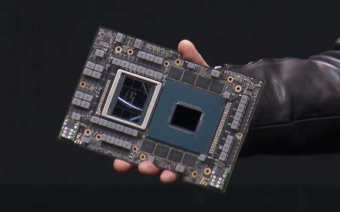
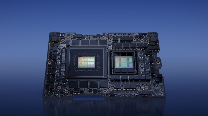
Teeing off an AI-heavy slate of announcements for NVIDIA, the company has confirmed that their Grace Hopper “superchip” has entered full production. The combination of a Grace CPU and Hopper H100 GPU, Grace Hopper is designed to be NVIDIA’s answer for customers who need a more tightly integrated CPU + GPU solution for their workloads – particularly for AI models.


In the works for a few years now, Grace Hopper is NVIDIA’s efforts to leverage both their existing strength in the GPU space and newfound efforts in the CPU space to deliver a semi-integrated CPU/GPU product unlike anything their top-line competitors offer. With NVIDIA’s traditional dominance in the GPU space, the company has essentially been working backwards, combining their GPU technology with other types of processors (CPUs, DPUs, etc) in order to access markets that benefit from GPU acceleration, but where fully discrete GPUs may not be the best solution.


NVIDIA Grace Hopper Specifications
  Grace Hopper (GH200)
CPU Cores 72
CPU Architecture Arm Neoverse V2
CPU Memory Capacity <=480GB LPDDR5X (ECC)
CPU Memory Bandwidth <=512GB/sec
GPU SMs 132
GPU Tensor Cores 528
GPU Architecture Hopper
GPU Memory Capcity <=96GB
GPU Memory Bandwidth <=4TB/sec
GPU-to-CPU Interface 900GB/sec

NVLink 4
TDP 450W – 1000W
Manufacturing Process TSMC 4N
Interface Superchip


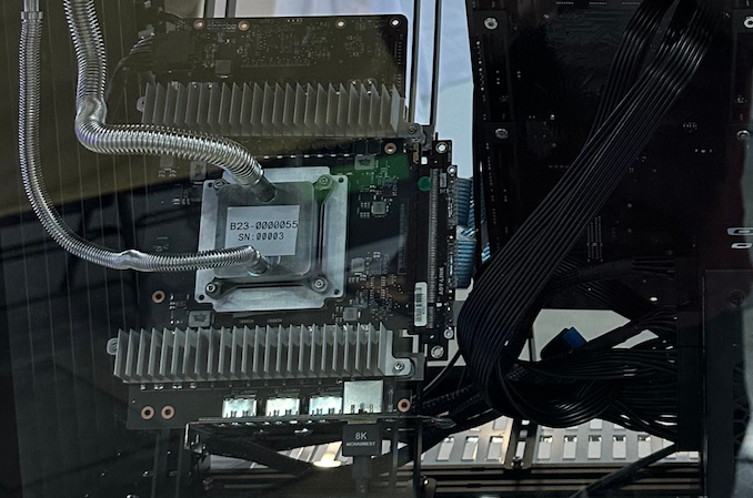
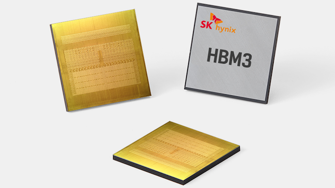
In this first NVIDIA HPC CPU + GPU mash-up, the Hopper GPU is the known side of the equation. While it only started shipping in appreciable volumes this year, NVIDIA was detailing the Hopper architecture and performance expectations over a year ago. Based on the 80B transistor GH100 GPU, H100 brings just shy of 1 EFLOPS of FP16 matrix math throughput for AI workloads, as well as 80GB of HBM3 memory. H100 is itself already a huge success – thanks to the explosion of ChatGPT and other generative AI services, NVIDIA is already selling everything they can make – but NVIDIA is still pushing ahead with their efforts to break into markets where the workloads require closer CPU/GPU integration.


Being paired with H100, in turn, is NVIDIA’s Grace CPU, which itself just entered full production a couple of months ago. The Arm Neoverse V2-based chip packs 72 CPU cores, and comes with up to 480GB of LPDDR5X memory. And while the CPU cores are themselves plenty interesting, the bigger twist with Grace has been NVIDIA’s decision to co-package the CPU with LPDDR5X, rather than using slotted DIMMs. The on-package memory has allowed NVIDIA to use both higher clocked and lower power memory – at the cost of expandability – which makes Grace unlike any other HPC-class CPU on the market. And potentially a very big deal for Large Language Model (LLM) training, given the emphasis on both dataset sizes and the memory bandwidth needed to shuffle that data around.


It’s that data shuffling, in turn, that helps to define a single Grace Hopper board as something more than just a CPU and GPU glued together on the same board. Because NVIDIA equipped Grace with NVLink support – NVIDIA’s proprietary high-bandwidth chip interconnect – Grace and Hopper have a much faster interconnect than a traditional, PCIe-based CPU + GPU setup. The resulting NVLink Chip-to-Chip (C2C) link offers 900GB/second of bandwidth between the two chips (450GB/sec in each direction), giving Hopper the ability to talk back to Grace even faster than Grace can read or write to its own memory.


The resulting board, which NVIDIA calls their GH200 “superchip”, is meant to be NVIDIA’s answer to the AI and HPC markets for the next product cycle. For customers who need a more local CPU than a traditional CPU + GPU setup – or perhaps more pointedly, more quasi-local memory than a stand-alone GPU can be equipped with – Grace Hopper is NVIDIA’s most comprehensive compute product yet. Meanwhile, with there being some uncertainty over just how prevalent the Grace-only (CPU-only) superchip will be, given that NVIDIA is currently on an AI bender, Grace Hopper may very well end up being where we see the most of Grace, as well.


According to NVIDIA, systems incorporating GH200 chips are slated to be available later this year.


DGX GH200 AI Supercomputer: Grace Hopper Goes Straight To the Big Leagues


Meanwhile, even though Grace Hopper is not technically out the door yet, NVIDIA is already at work building its first DGX system around the chip. Though in this case, “DGX” may be a bit of a misnomer for the system, which unlike other DGX systems isn’t a single node, but rather a full-on multi-rack computational cluster – hence NVIDIA terming it a “supercomputer.”


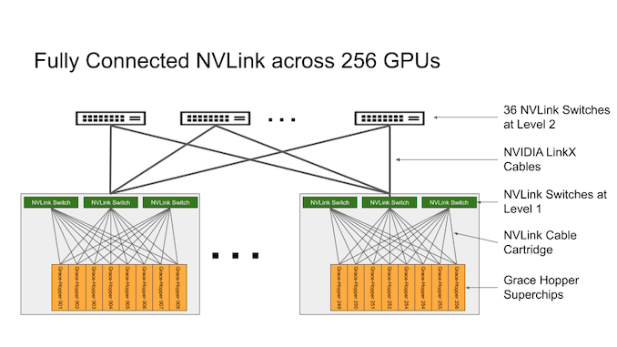
At a high level, the DGX GH200 AI Supercomputer is a complete, turn-key, 256 node GH200 cluster. Spanning some 24 racks, a single DGX GH200 contains 256 GH200 chips – and thus, 256 Grace CPUs and 256 H100 GPUs – as well as all of the networking hardware needed to interlink the systems for operation. In cumulative total, a DGX GH200 cluster offers 120TB of CPU-attached memory, another 24TB of GPU-attached memory, and a total of 1 EFLOPS of FP8 throughput (with sparsity).


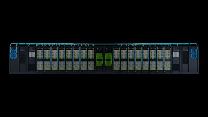
Look Closer: That’s Not a Server Node – That’s 24 Server Racks


Linking the nodes together is a two-layer networking system built around NVLink. 96 local, L1 switches provide immediate communications between the GH200 blades, while another 36 L2 switches provide a second layer of connectivity tying together the L1 switches. And if that’s not enough scalability for you, DGX GH200 clusters can be further scaled up in size by using InfiniBand, which is present in the cluster as part of NVIDIA’s use of ConnectX-7 network adapters.


The target market for the sizable silicon cluster is training large AI models. NVIDIA is leaning heavily on their existing hardware and toolsets in the field, combined with the sheer amount of memory and memory bandwidth a 256-node cluster affords to be able to accommodate some of the largest AI models around. The recent explosion in interest in large language models has exposed just how much memory capacity is a constraining factor, so this is NVIDIA’s attempt to offer a single-vendor, integrated solution for customers with especially large models.


And while not explicitly disclosed by NVIDIA, in a sign that they all pulling out all of the stops for the DGX GH200 cluster, the memory capacities they’ve listed indicate that NVIDIA isn’t just shipping regular H100 GPUs as part of the system, but rather they are using their limited availability 96GB models, which have the normally-disabled 6th stack of HBM3 memory enabled. So far, NVIDIA only offers these H100 variants in a handful of products – the specialty H100 NVL PCIe card and now in some GH200 configurations – so DGX GH200 is slated to get some of NVIDIA’s best silicon.


Of course, don’t expect a supercomputer from NVIDIA to come cheaply. While NVIDIA is not announcing any pricing this far in advance, based on HGX H100 board pricing (8x H100s on a carrier board for $200K), a single DGX GH200 is easily going to cost somewhere in the low 8 digits. Suffice it to say, DGX GH200 is aimed at a rather specific subset of Enterprise clientele – those who need to do a lot of large model training and have the deep pocketbooks to pay for a complete, turn-key solution.


Ultimately, however, DGX GH200 isn’t just meant to be a high-end system for NVIDIA to sell to deep-pocketed customers, but it’s the blueprint for helping their hyperscaler customers build their own GH200-based clusters. Building such a system is, after all, the best way to demonstrate how it works and how well it works, so NVIDIA is forging their own path in this regard. And while NVIDIA would no doubt be happy to sell a whole lot of these DGX systems directly, so long as it gets hyperscalers, CSPs, and others adopting GH200 in large numbers (and not, say, rival products), then that’s still going to be a win in NVIDIA’s books.


In the meantime, for the handful of businesses that can afford a DGX GH200 AI Supercomputer, according to NVIDIA the systems will be available by the end of the year.


Source: AnandTech – NVIDIA: Grace Hopper Has Entered Full Production & Announcing DGX GH200 AI Supercomputer

Arm Unveils 2023 Mobile CPU Core Designs: Cortex-X4, A720, and A520 – the Armv9.2 Family

Throughout the world, if there’s one universal constant in the smartphone and mobile device market, it’s Arm. Whether it’s mobile chip makers basing their SoCs on Arm’s fully synthesized CPU cores, or just relying on the Arm ISA and designing their own chips, at the end of the day, Arm underlies virtually all of it. That kind of market saturation and relevance is a testament to all of the hard work that Arm has done in the last few decades getting to this point, but it’s also a grave responsibility – for most mobile SoCs, their performance only moves forward as quickly as Arm’s own CPU core designs and associated IP do.


Consequently, we’ve seen Arm settle into a yearly cadence for their client IP, and this year is no exception. Timed to align with this year’s Computex trade show in Taiwan, Arm is showing off a new set of Cortex-A and Cortex-X series CPU cores – as well as a new generation of GPU designs – which we’ll see carrying the torch for Arm starting later this year and into 2024. These include the flagship Cortex-X4 core, as well as Arm’s mid-core Cortex-A720. and the new little-core Cortex-A520.


Arm’s latest CPU cores build upon the foundation of Armv9 and their Total Compute Solution (TSC21/22) ecosystem. For their 2023 IP, Arm is rolling out a wave of minor microarchitectural improvements through its Cortex line of cores with subtle changes designed to push efficiency and performance throughout, all the while moving entirely to the AArch64 64-bit instruction set. The latest CPU designs from Arm are also designed to align with the ongoing industry-wide drive towards improved security, and while these features aren’t strictly end-user facing, it does underscore how Arm’s generational improvements are to more than just performance and power efficiency.


In addition to refining its CPU cores, Arm has undertaken a comprehensive upgrade of its DynamIQ Shared Unit core complex block, with the DSU-120. Although the modifications introduced are subtle, they hold substantial significance in terms of improving the efficiency of the fabric holding Arm CPU cores together, along with extending Arm’s reach even further in terms of performance scalability with support for up to 14 CPU cores in a single block – a move designed to make Cortex-A/X even better suited for laptops.


Source: AnandTech – Arm Unveils 2023 Mobile CPU Core Designs: Cortex-X4, A720, and A520 – the Armv9.2 Family

TSMC Preps 6x Reticle Size Super Carrier Interposer for Extreme SiP Processors

As part of their efforts to push the boundaries on the largest manufacturable chip sizes, Taiwan Semiconductor Manufacturing Co. is working on its new Chip-On-Wafer-On-Substrate-L (CoWoS-L) packaging technology that will allow it to build larger Super Carrier interposers. Aimed at the 2025 time span, the next generation of TSMC’s CoWoS technology will allow for interposers reaching up to six times TSMC’s maximum reticle size, up from 3.3x for their current interposers. Such formidable system-in-packages (SiP) are intended for use by performance-hungry data center and HPC chips, a niche market that has proven willing to pay significant premiums to be able to place multiple high performance chiplets on a single package.


“We are currently developing a 6x reticle size CoWoS-L technology with Super Carrier interposer technology,” said said Yujun Li, TSMC’s director of business development who is in charge of the foundry’s High Performance Computing Business Division, at the company’s European Technology Symposium 2023.


Global megatrends like artificial intelligence (AI) and high-performance computing (HPC) have created demand for seemingly infinite amounts of compute horsepower, which is why companies like AMD, Intel, and NVIDIA are building extremely complex processors to address those AI and HPC applications. One of the ways to increase compute capabilities of processors is to increase their transistor count; and to do so efficiently these days, companies use multi-tile chiplet designs. Intel’s impressive, 47 tile Ponte Vecchio GPU is a good example of such designs; but TSMC’s CoWoS-L packaging technology will enable the foundry to build Super Carrier interposers for even more gargantuan processors.


The theoretical EUV reticle limit is 858mm(26 mm by 33 mm), so six of these masks would enable SiPs of 5148 mm2. Such a large interposer would not only afford room for multiple large compute chiplets, but it also leaves plenty of room for things like 12 stacks of HBM3 (or HBM4) memory, which means a 12288-bit memory interface with bandwidth reaching as high as 9.8 TB/s.


“The Super Carrier interposer features multiple RDL layers on the front as well as on the backside of the interposer for yield and manufacturability,” explained Li. “We can also integrate various passive components in the interpreter for performance. This six reticle-size CoWoS-L will be qualified in 2025”


Building 5148 mm2 SiPs is an extremely tough tasks and we can only wonder how much they will cost and how much their developers will charge for them. At present NVIDIA’s H100 accelerator, whose packaging spans an interposer multiple reticles in size, costs around $30,000. So a considerable larger and more powerful chip would likely push prices higher still.


But paying for the cost of large processors will not be the only huge investments that data center operators will need to make. The amount of active silicon that 5148 mm2 SiPs can house will almost certainly result in some of the most power-hungry HPC chips produced yet – chips that will also need equally powerful liquid cooling to match. To that end, TSMC has disclosed that it has been testing on-chip liquid cooling technology, stating that it has managed to cool down silicon packages with power levels as high as 2.6 kW. So TSMC does have some ideas in mind to handle the cooling need of these extreme chips, if only at the price of integrating even more cutting-edge technology.


Source: AnandTech – TSMC Preps 6x Reticle Size Super Carrier Interposer for Extreme SiP Processors

TSMC Details N4X Process for HPC: Extreme Performance at Minimum Leakage

At its 2023 Technology Symposium TSMC revealed some additional details about its upcoming N4X technology that is designed specifically for high-performance computing (HPC) applications. This node promises to enable ultra-high performance and improve efficiency while maintaining IP compatibility with N4P (4 nm-class) process technology.


“N4X truly sets a new benchmark for how we can push extreme performance while minimizing the leakage power penalty,” said Yujun Li, TSMC’s director of business development who is in charge of the foundry’s High Performance Computing Business Division.


TSMC’s N4X technology belongs to the company’s N5 (5 nm-class) family, but it is enhanced in several ways and is optimized for voltages of 1.2V and higher in overdrive mode.


To achieve higher performance and efficiency, TSMC’s N4X improves transistor design in three three key areas. Firstly, they refined their transistors to boost both processing speed and drive currents. Secondly, the foundry incorporated its new high-density metal-insulator-metal (MiM) capacitors, to provide reliable power under high workloads. Lastly, they modified the the back-end-of-line metal stack to provide more power to the transistors.


In particular, N4X adds four new devices on top of the N4P device offerings, including ultra-low-voltage transistors (uLVT) for applications that need to be very efficient, and extremely-low threshold voltage transistors  (eLVT) for applications that need to work at high clocks. For example, N4X uLVT with overdrive offers 21% lower power at the same speed when compared to N4P eLVT, whereas N4X eLVT in OD offers 6% higher speed for critical paths when compared to N4P eLVT.


Advertised PPA Improvements of New Process Technologies

Data announced during conference calls, events, press briefings and press releases
  TSMC
N5

vs

N7
N5P

vs

N5
N5HPC

vs

N5
N4

vs

N5
N4P

vs

N5
N4P

vs

N4
N4X

vs

N5
N4X

vs

N4P
N3

vs

N5
Power -30% -10% ? lower -22% ? ? -25-30%
Performance +15% +5% +7% higher +11% +6% +15%

or

more
+4%

or more
+10-15%
Logic Area


Reduction %


(Density)
0.55x


-45%


(1.8x)


0.94x


-6%


1.06x
0.94x


-6%


1.06x


?


?
0.58x


-42%


(1.7x)
Volume

Manufacturing
Q2 2020 2021 Q2 2022 2022 2023 H2 2022 H1

2024?
H1 2024? H2 2022


While N4X offers significant performance enhancements compared to N4 and N4P, it continues to use the same SRAM, standard I/O, and other IPs as N4P, which enables chip designers to migrate their designs to N4X easily and cost effectively. Meanwhile, keeping in mind N4X’s IP compatibility with N4P, it is logical to expect transistor density of N4X to be more or less in line with that of N4P. Though given the focus of this technology, expect chip designers to use this technology to get extreme performance rather than maximum transistor density and small chip dimensions.


TSMC claims that N4X has achieved its SPICE model performance targets, so customers can start using the technology today for their HPC designs that will enter production sometimes next year.


For TSMC, N4X is an important technology as HPC designs are expected to be the company’s main revenue growth driver in the coming years. The contract maker of chips anticipates HPC to account for 40% of its revenue in 2030 followed by smartphones (30%) and automotive (15%) applications.


Source: AnandTech – TSMC Details N4X Process for HPC: Extreme Performance at Minimum Leakage

NVIDIA Reports Q1 FY2024 Earnings: Bigger Things to Come as NV Approaches $1T Market Cap

Closing out the most recent earnings season for the PC industry is, as always, NVIDIA. The company’s unusual, nearly year-ahead fiscal calendar means that they get the benefit of being casually late in reporting their results. And in this case, they’ve ended up being the proverbial case of saving the best for last.

For the first quarter of their 2024 fiscal year, NVIDIA booked $7.2 billion in revenue, which is a 13% drop over the year-ago quarter. Like the rest of the chip industry, NVIDIA has been weathering a significant slump in demand for computing products over the past few quarters, which in turn has dented NVIDIA’s revenue and profitability. However, while NVIDIA’s consumer-focused gaming division has continued to take matters on the chin, the strong performance of NVIDIA’s data center group has kept the company as a whole fairly profitable, with the most recent quarter setting a segment record and helping NVIDIA to avoid the tough financial situations faced by rivals AMD and Intel.

NVIDIA Q1 FY2024 Financial Results (GAAP)
  Q1 FY2024 Q4 FY2023 Q1 FY2023 Q/Q Y/Y
Revenue $7.2B $6.1B $8.3B +19% -13%
Gross Margin 64.6% 63.3% 65.5% +1.3ppt -0.9ppt
Operating Income $2.1B $1.3B $1.9B +70% +15%
Net Income $2.0B $1.4B $1.6B +44% +26%
EPS $0.82 $0.57 $0.64 +44% +28%

To that end, while Q1’FY24 was not by any means a record quarter for NVIDIA, it was still a relatively strong one for the company. NVIDIA’s net income of $2 billion makes for one of their better quarters in that regard, and it’s actually up 26% year-over-year despite the revenue drop. That said, reading between the lines will find that NVIDIA paid their Arm acquisition breakup fee last year (Q1’FY23), so NVIDIA’s GAAP net income looks a bit better than it otherwise would; while non-GAAP net income would be down 21%. Meanwhile, NVIDIA’s gross margins have held strong in the most recent quarter, with NVIDIA posting a GAAP gross margin of 64.6%.

But even a solid quarter during an industry slump is arguably not the biggest news to come out of NVIDIA’s most recent earnings report. Rather, it’s the company’s projections for Q2’FY24. In short, NVIDIA is expecting revenue to explode in Q2, with the company forecasting $11 billion in sales. Should it come to fruition, such a quarter would blow well past NVIDIA’s previous revenue records – and shattering Wall Street expectations. As a result, NVIDIA’s stock has already taken off in overnight trading, and by the time the market opens a bit later this morning, NVIDIA is expected to be a $930B+ company, knocking on the door of crossing a market capitalization of a trillion dollars.


Source: AnandTech – NVIDIA Reports Q1 FY2024 Earnings: Bigger Things to Come as NV Approaches T Market Cap

TSMC: We Have Working CFET Transistors in the Lab, But They Are Generations Away

Offering an update on its work with complementary field-effect transistors (CFETs) as part of the company’s European Technology Symposium 2023, TSMC has revealed that it has working CFETs within its labs. But even with the progress TSMC has made so far, the technology is still in its early days, generations away from mass production. In the meantime, ahead of CFETs will come gate-all-around (GAA) transistors, which TSMC will be introducing with its TSMC’s upcoming N2 (2nm-class) production nodes.


One of TSMC’s long-term bets as the eventual successor to GAAFETs, CFETs are expected to offer advantages over GAAFETs and FinFETs when it comes to power efficiency, performance, and transistor density. However, these potential benefits are theoretical and dependent on overcoming significant technical challenges in fabrication and design. In particular, CFETs are projected to require the usage of extremely precise lithography (think High NA EUV tools) to integrate both n-type and p-type FETs into a single device, as well as determining the most ideal materials to ensure appropriate electronic properties. 


Just like other chip fabs, TSMC is working on a variety of transistor design types, so having CFETs working in the lab is important. But it’s also not something that is completely unexpected; researchers elsewhere have previously assembled CFETs, so now it’s up to industry-focused TSMC to figure out how to bring about mass production. To that end, TSMC is stressing that CFETs are not in the near future.


“Let me make a clarification on that roadmap, everything beyond the nanosheet is something we will put on our [roadmap] to tell you there is still future out there,” said Kevin Zhang, senior vice president at responsible for technology roadmap, business strategy. “We will continue to work on different options. I also have the add on to the one-dimensional material-[based transistors] […], all of those are being researched on being investigated on the future potential candidates right now, we will not tell you exactly the transistor architecture will be beyond the nanosheet.”


Indeed, research projects take a long time and when you are running many of them in parallel, you never know which of them comes to fruition. Even at that point, it is hard to tell which of potential structure candidates TSMC (or any other fabs) will choose, Ultimately, fabs have to meet the needs of their larger customers (e.g., Apple, AMD, MediaTek, Nvidia, Qualcomm) at the time when this production node is ready for high volume manufacturing.


To that end, TSMC is going to use GAA structures for years to come, according to Zhang.


“Nanosheet is starting at 2nm, it is reasonable to project and that nanosheet will be used for at least a couple of generations, right,” asked Zhang rhetorically. “So, if you think about CFETs, we’ve leveraged [FinFETs] for five generations, which is more than 10 years. Maybe [device structure] is somebody else’s problem to worry, then you can continue to write a story.”


Source; TSMC European Technology Symposium 2023


Source: AnandTech – TSMC: We Have Working CFET Transistors in the Lab, But They Are Generations Away

Corsair Launches 2000D Airflow SFF Cases For Triple-Slot GPUs

Corsair has expanded the brand’s mini-ITX case lineup with the new 2000D Airflow series. The 2000D Airflow and 2000D RGB Airflow small-form-factor (SFF) cases cater specifically to compact but high-performance systems. With a volume of 24.4 liters, the Corsair 2000D series cases have enough landscape to house the most demanding hardware, including a 360 mm AIO CPU liquid cooler and full-size graphics cards up to a triple-slot design.


The 2000D Airflow is available with and without RGB-lit fans and in white or black colors. Therefore, the case comes in four different variants. Regardless, the 2000D Airflow is a mini-ITX case that prioritizes airflow for the components housed inside. For this same reason, Corsair designs the 2000D Airflow with removable steel mesh front, side, and rear panels for maximum ventilation from all directions. The case measures 18.03 x 10.67 x 7.87 inches and weighs just under 10 pounds. As a result, it doesn’t require much space whether users decide to put it on or under the desk. Being an SFF case, the 2000D Airflow only accepts mini-ITX motherboards.


The 2000D Airflow can accommodate up to eight 120 mm and two 140 mm cooling fans, doing the case’s name justice. If a user fits the 2000D Airflow with a single-slot graphics card, it opens the possibility of cooling the graphics card with two additional fan mounts. For CPU air cooling enthusiasts, the 2000D Airflow supports coolers with a maximum height of up to 6.69 inches. Given the generous amount of fan mounts, Corsair’s SFF case offers plentiful liquid cooling options. It supports 120 mm, 140 mm, 240 mm, 280 mm, and 360 mm radiators. Users can fit up to multiple radiators with an example combination of a 360 mm unit on the side and a 240 mm one at the rear in a scenario with a single-slot graphics card.


The 2000D Airflow has three case expansion slots, accommodating beefy graphics cards with up to three PCI slots in a vertical orientation. Consumers will have no problem fitting a GeForce RTX 4090 into the 2000D Airflow. However, they must ensure the graphics card is shorter than 14.37 inches since that’s the maximum length permitted inside the 2000D Airflow.


Storage options, however, are limited to three 2.5-inch drives, whether SSDs or hard drives, with the 2000D Airflow. In addition, one of the case’s caveats is that it only accepts SFX or SFL-L power supplies, reducing options to units with a length of up to 5.12 inches. Nevertheless, Corsair aficionados will have no issues finding an adequate unit within the brand’s ecosystem since the company offers the SF series and SF-L series with capacities varying from 600 watts to 750 watts on the former and 850 watts to 1,000 watts on the latter. Regarding the I/O design, the 2000D Airflow offers one USB 3.2 Gen 2 Type-C port, two USB 3.2 Gen 1 Type-A ports, and one 3.5 mm audio jack on the front panel.


The 2000D Airflow retails for $139.99. On the other hand, the 2000D RGB Airflow, which has three pre-installed Corsair AF120 RGB Slim fans in the front intake, will set consumers back $199.99. Corsair backs its 2000D Airflow cases with a two-year warranty. In the case of the RGB variant, the AF120 RGB Slim fans come with a three-year warranty.


Source: AnandTech – Corsair Launches 2000D Airflow SFF Cases For Triple-Slot GPUs

AMD Launches Zen 2-based Ryzen and Athlon 7020C Series For Chromebooks

Last year, AMD unveiled their entry-level ‘Mendicino’ mobile parts to the market, which combine their 2019 Zen 2 cores and their RDNA 2.0 integrated graphics to create an affordable selection of configurations for mainstream mobile devices. Although much of the discussion over the last few months has been about their Ryzen 7040 mobile parts, AMD has launched four new SKUs explicitly designed for the Chromebook space, the Ryzen and Athlon 7020C series.

Some of the most notable features of AMD’s Ryzen/Athlon 7020C series processors for Chromebooks include three different configurations of cores and threads, ranging from entry-level 2C/2T up to 4C/8T, all with AMD’s RDNA 2-based Radeon 610M mobile integrated graphics. Designed for a wide variety of tasks and users, including and not limited to consumers, education, and businesses, AMD’s Ryzen 7020C series looks to offer similar specifications and features to their regular 7020 series mobile parts but expands things to the broader Chromebook and ChromeOS ecosystem too.


Source: AnandTech – AMD Launches Zen 2-based Ryzen and Athlon 7020C Series For Chromebooks