MLperf is an up-and-coming benchmark aimed at machine learning, backed by a number of industry leaders in this area.
Source: AnandTech – Hot Chips 31 Live Blogs: MLperf Benchmark
MLperf is an up-and-coming benchmark aimed at machine learning, backed by a number of industry leaders in this area.
Source: AnandTech – Hot Chips 31 Live Blogs: MLperf Benchmark
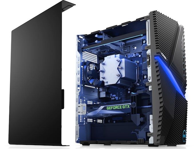
Historically, Dell has addressed the market for higher-end gaming desktops with their Alienware-branded machines, which are frequently built around unlocked CPUs as well as advanced graphics cards. Meanwhile, for those who wanted Dell-branded gaming PCs without the Alienware premium, the company has offered their custom-built Inspiron as well as XPS-branded machines; though there’s a large gap between the premium XPS and basic Inspiron as well. So, looking to bridge the gap between their machines and produce a line of gaming-centric yet still reasonably affordable desktops, at this year’s Gamescom the company is introducing its first ever Dell G-series desktops. Taking their name from Dell’s popular G5 gaming laptops – which are intended to fill much the same role on the laptop side – these new machines are intended to be Dell’s gaming-focused desktops for the wider market.
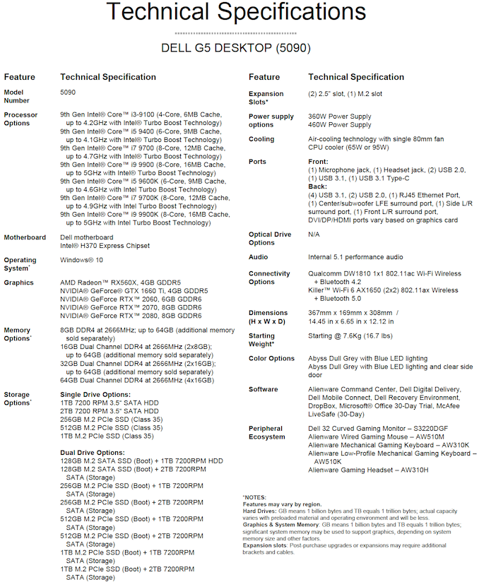
The Dell G5 desktop (model 5090) is based on Intel’s 9th Generation Core processors and is paired with AMD’s Radeon RX 5700-series or NVIDIA’s GeForce GTX 1660 Ti or RTX 2000-series graphics cards. In its top-of-the-range configuration, the Dell G5 can pack Intel’s Core i9-9900K processor, NVIDIA’s GeForce RTX 2080 GPU, 64 GB of DDR4-2666 memory, a 1 TB M.2 PCIe SSD, a 2 TB hard drive (or two of them), a Killer Wi-Fi 6 AX1650 network card, Gigabit Ethernet, and so on.
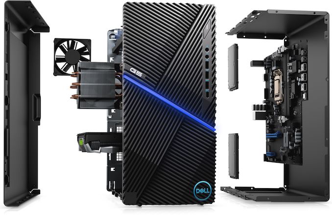
Dell emphasizes that its compact G5 desktop is completely user-upgradeable, so owners will be able to easily install a new graphics card or upgrade to more storage when they need to. Meanwhile, since the machine uses a motherboard based on Intel’s H370 chipset, it does not support CPU overclocking, unlike Alienware-branded computers. The lack of overclocking support also means that Dell can stick with a (relatively) conservative 480 Watt power supply for the system, as there’s no need for a bunch of overclocking headroom in the power delivery design. Overall, this is enough for a 9900K CPU paired up with one of NVIDIA’s GeForce RTX 2080 video cards, but is likely a factor in why we don’t see an RTX 2080 Ti here.
![]()
Unlike many gaming desktops these days, Dell’s G5 will not come with liquid cooling, but will rely on proven air cooling systems with heat pipes. Keeping in mind that CPU overclocking is not supported by the platform, air cooling should be plenty sufficient. Meanwhile, those who would like CPU and GPU to at least hit their maximum boost clocks more often can set appropriate thermal profiles in the Alienware Command Center software.
Dell’s G5 desktops will be available starting August 19. Prices will start at $629, with more advanced configurations coming in at higher prices.
Related Reading:
Source: Dell
Source: AnandTech – Dell Unveils G5 Gaming Desktop: Starting at 9

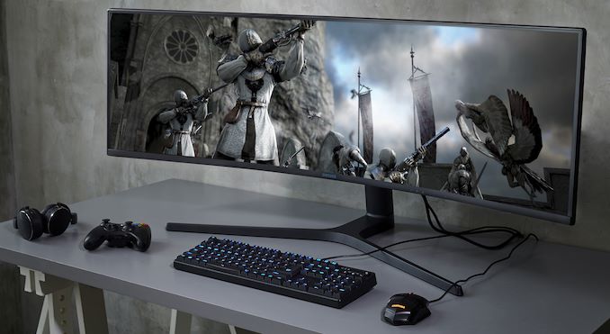
Today at Gamescom, Dell has officially launched its new flagship OLED gaming monitor, the Alienware 55. First demonstrated back at Computex, the display uses a 4K OLED panel featuring a 120 Hz refresh rate, making it among the fastest 4K monitors available. The Alienware 55 supports AMD’s FreeSync variable refresh rate technology, which is what sets the monitor apart from OLED UHDTVs, yet not in its HDR implementation.
The Alienware 55 is based on a 55-inch OLED panel featuring a 3840×2160 resolution, 400 nits peak brightness, a 130,000:1 contrast ration, a 0.5 ms gray to gray response time, as well as a 120 Hz maximum refresh rate. The screen can reproduce 98.5% of the DCI-P3 color gamut, which is comparable to accuracy of professional LCD displays. The monitor also has an anti-reflective coating with 2H hardness for additional clarity when used in bright days.

The key feature set of the Alienware 55 is a combination of its technologies as well as its size. OLED computer displays are rare in general, and this one is the industry’s first OLED monitors for gamers. The product is not without caveats though: despite the use of OLED technoloy, this is not an HDR monitor. In fact, Dell says nothing about Alienware’s 55-incher supporting HDR10 or Dolby Vision transports; so regardless of what the panel can do, it would appear that the monitor itself doesn’t support any HDR input formats.
| Alienware 55 (AW5520QF) Display Specifications | ||
| Panel | 55-inch OLED | |
| Resolution | 3840 × 2160 | |
| Refresh Rate | 120 Hz | |
| Response Time | 0.5 ms gray-to-gray | |
| Brightness | Peal: 400 cd/m² | |
| Contrast | 130,000:1 | |
| Viewing Angles | 120°/120° horizontal/vertical | |
| Color Saturation | 98.5% DCI-P3 | |
| Display Colors | 1.07 billion | |
| 3D-LUT | ? bits | |
| Pixel Pitch | 0.3108 mm² | |
| Pixel Density | 81 PPI | |
| Anti-Glare Coating | 2H | |
| Inputs | 1 × DP 1.2 4 × HDMI 2.0 |
|
| USB Hub | Quad-port USB 3.1 Gen 1 hub | |
| Audio | 2 × 14 W speakers 3.5-mm mini jack S/PDIF |
|
| Mechanical Design | Chassis Colors: black, metallic, AlienFX RGB lighting |
|
| Power Consumption | Idle | 0.3 W |
| Active | 100 W ~ 390 W | |
The Alienware 55 comes with three HDMI 2.0 inputs as well as one DisplayPort 1.2 connector, with the latter being the second oddity in today’s announcement. With full 4:4:4/RGB color, DisplayPort 1.2 is limited to 60Hz; you need DisplayPort 1.4 for 4K@120Hz with 8bpc color. So for what Dell is doing, there’s an error in the specifications or compromise somewhere. Either DisplayPort 1.2 is right and they’re doing something akin to 4:2:2 choma subsampling to make 120Hz work, or this is not a true 120Hz monitor at all – and instead it’s a 60Hz monitor with black frame insertion, a common tactic for TVs. At this point we’re not sure which it is, and we’ve reached out to Dell for clarification.
Moving on, the display has a quad-port USB 3.1 Gen 1 hub, a headphone output, and an S/PDIF line out. When it comes to audio, the display has two 14 W speakers that were co-designed with Wave Maxx Audio.
Just like other large displays, the Alienware 55 comes with a remote control to adjust brightness, regulate audio and perform other operations.

Dell will start sales of the Alienware 55 display starting September 30 at $3,999.99.

Related Reading:
Source: Dell
Source: AnandTech – Dell Launches 55-Inch Alienware OLED Display: 4K at 120 Hz with Deep Blacks
The keynote for day one at Hot Chips is from Dr. Lisa Su, AMD of CEO. AMD is riding high after successful Ryzen 3000 and 2nd Gen EPYC Rome launches, so it will be interesting to hear what she has to say. Come back at 1:45pm PT (4:45pm ET) to read our live blog.
Source: AnandTech – Hot Chips 31 Keynote Day 1: Dr. Lisa Su, CEO of AMD Live Blog (1:45pm PT)
This year at Hot Chips, Intel is presenting the latest updates to its Optane PCDMM strategy.
Source: AnandTech – Hot Chips 31 Live Blogs: Intel Optane
Princeton is presenting it’s own solution for in-memory compute this year at Hot Chips.
Source: AnandTech – Hot Chips 31 Live Blogs: Princeton In-Memory Compute Embedded CPU
One of the key critical future elements about this world of compute is moving data about. Moving data requires power, to the point where calling data from memory can consume more power than actually doing ‘compute’ work on it. This is why we have caches, but even these require extensive management built in to the CPU. For simple operations, like bit-shifts or AND operations, the goal is to move the ability to do that compute onto the main DRAM itself, so it doesn’t have to shuttle back and forth. This year at Hot Chips, UPMEM is one of the first companies to showcase their new technology.
Source: AnandTech – Hot Chips 31 Analysis: In-Memory Processing by UPMEM
We’re here at Hot Chips 31 / 2019, and the first talk to be live blogged is IBM’s newest variant of its POWER CPUs. This talk starts at 10am PT / 1pm ET – come back then for all the details.
Source: AnandTech – Hot Chips 31 Live Blogs: IBM’s Next Generation POWER

Micron this week hosted a grand opening ceremony of its Fab 10 Expansion in Singapore. The new cleanroom is not expected to increase the company’s production capacity in terms of wafer starts per month, but will enable Micron to continue adopting more advanced 3D NAND process technologies with a higher number of layers and bit density.
The new Fab 10 Expansion is an integral part of Micron’s Fab 10 complex that was previously comprised of Fab 10N and Fab 10X. Officially, it’s known that the new 3D NAND production facility is built on a 165,000 m2 land plot, however Micron is not disclosing much else about the usable cleanroom space or other features of the expansion.

Micron is now installing equipment and expects to start production of 96-layer 3D NAND at the new Fab 10 Expansion sometime in the second half of this calendar year (i.e. in the next 4.5 months). Meanwhile, the company stresses that it will align its spending on production tools with 3D NAND demand and trends. Furthermore, even when fully equipped, the facility is not expected to add any new wafer capacity, but rather will be used to house more advanced process equipment necessary for greater numbers of 3D NAND layers.
As the number of 3D NAND layers increases, each wafer has to spend more time inside chemical vapor deposition (CVD) machines, meaning it takes longer to etch them. Adding more time still, various extravagant production techniques like string stacking lengthen manufacturing require even more steps. In order to keep the number of wafers processed consistent as the number of 3D NAND layers grows, flash memory producers have to add extra CVD and etching machines to cleanrooms, which requires extra space. As a result, while bigger fabs may not increase the number of wafer starts per month, they do enable growth in terms of produced NAND flash bits.

Along with the new manufacturing plant, Micron is also expanding its R&D operations in Singapore. Micron’s NAND Center of Excellence will among other things perform technology development and product engineering. Considering how close these functions will be to the actual production facility, the company certainly hopes to improve its yields and productivity at Fab 10.
Related Reading:
Sources: Micron, The Strait Times
Source: AnandTech – Micron’s Fab 10 Expansion Completed: 96-Layer 3D NAND Production Starts in 2019

SMIC, the largest contract maker of semiconductors in China, announced this month that it would start commercial production of chips using its 14 nm FinFET manufacturing technology by the end of the year. This is the first FinFET manufacturing line in China, making it a notable development for a country that already houses a significant number of fabs, as the world’s leading-edge manufacturers never installed FinFET technology in China for geopolitical and IP reasons. SMIC in turn seems to expect a rather rapid ramp of its 14 nm node, as it anticipates the new manufacturing line will meaningfully contribute to its revenue before the end of the year.
According to SMIC, their 14 nm FinFET manufacturing technology was developed entirely in-house and is expected to significantly increase transistor density, increase performance, and lower power consumption of chips when compared to devices made using the company’s 28 nm process that relies on planar transistors. Earlier this year it was expected that SMIC would start production of 14 nm chips already in the first half of 2019, so the firm seems to be a little behind the schedule. Nonetheless, an in-house FinFET process technology is quite a breakthrough for a relatively small company that puts it into a club with just five other foundries with FinFET technologies.
One interesting thing that SMIC said about its 14 nm FinFET volume ramp is that it expects the process to have a significant revenue contribution already by the end of the year. Meanwhile, keeping in mind that right now SMIC only has two relatively small 300-mm HVM fabs (which are currently used for 28 nm – 65 nm nodes) that are heavily utilized generating 40 ~ 49% of the company’s revenue (in Q1/Q2 2019), it is difficult to imagine SMIC making loads of 14 nm chips in 2019.
| Overview of SMIC’s Fabs | ||||
| Process Technologies | Capacity Wafer Starts per Month |
Location | ||
| BJ | 200mm | 90 nm – 150 nm | 50,000 | Beijing, China |
| 300mm | 28 nm – 65 nm | 35,000 | ||
| SH | 200 mm | 90 nm – 350 nm | 120,000 | Shanghai ,China |
| 300 mm | 28 nm – 65 nm | 20,000 | ||
| SZ | 200 mm | 90 nm – 350 nm | 60,000 | Shenzhen, China |
| 300 mm | 28 nm – 65 m | 3,000 | ||
| TJ | 200 mm | 90 nm – 350 nm | 50,000 | Tianjin, China |
| LF | 200 mm | 90 nm – 180 nm | 50,000 | Avezzano, Italy |
Earlier this year the company completed construction of its $10 billion SMIC South FinFET Fab, which will be used for its leading-edge manufacturing technologies and began moving in the equipment. Once the fab is ready for commercial operations, SMIC will be able to considerably increase production of chips using its 14 nm and then 12 nm FinFET fabrication technologies.

SMIC’s longer-term plans include 10 nm and 7 nm manufacturing processes. The latter is expected to require usage of extreme ultraviolet lithography tools, so last year SMIC acquired an EUV step-and-scan system from ASML for $120 million, which was to be delivered in 2019.
Related Reading:
Source: AnandTech – SMIC: 14nm FinFET in Risk Production; China’s First FinFET Line To Contribute Revenue by Late 2019
Micron announced on Thursday that it had started volume production of memory chips using its 3rd Generation 10 nm-class fabrication technology (also known as 1Z nm). The first DRAMs to be made using Micron’s 1Z nm process are 16 Gb monolithic DDR4 and LPDDR4X devices, with Micron expected to broaden their portfolio over time.
Micron’s 3rd Generation 10 nm-class (1Z nm) manufacturing process for DRAM will allow the company to increase the bit density, enhance the performance, and the lower power consumption of its DRAM chips as compared to its 2nd Generation 10 nm-class (1Y nm) technology. In particular, the company says that its 16 Gb DDR4 device consumes 40% less power than two 8 Gb DDR4 DRAMs (presumably at the same clocks). Meanwhile, Micron’s 16 Gb LPDDR4X ICs will bring an up to 10% power saving. Because of the higher bit density that the new 1Z nm technology provides, it will be cheaper for Micron to produce high-capacity (e.g., 16 Gb) memory chips for lower-cost, high-capacity memory sub-systems.
The manufacturer did not disclose the speed bins of its 16 Gb DDR4 DRAMs, but expect Micron to be in the official JEDEC ranges. One of the first products to use the company’s 16 Gb DDR4 devices will be high-capacity (e.g., 32 GB and higher) memory modules for desktops, notebooks, and workstations.
As for mobile memory, Micron’s 16 Gb LPDDR4X chips are rated for transfer rates up to 4266 MT/s. Furthermore, along with offering LPDDR4X DRAM packages with up to 16 GB (8x16Gb) of LPDDR4X for high-end smartphones, Micron will offer UFS-based multichip packages (uMCP4) that integrate NAND for storage and DRAM. The company’s uMCP4 family of products aimed at mainstream handsets will include offerings ranging from 64GB+3GB to 256GB+8GB (NAND+DRAM).
Micron did not disclose where it’s producing its monolithic 16 Gb DDR4 and LPDDR4X chips using its 1Z nm technology. Typically, the company kicks off volume production using its latest fabrication processes at its plant in Hiroshima, Japan. Meanwhile, there’s also been some speculation among analysts that the company is looking forward to running 1Z production lines this year at its Micron Memory Taiwan (former Rexchip Semiconductor) fab near Taichung, Taiwan.
Related Reading:
Source: Micron
Source: AnandTech – Micron: Mass Production of 16 Gb DDR4 & LPDDR4X Chips Using 1z nm Technology

Prior to Flash Memory Summit, Marvell unveiled their first generation of client SSD controllers supporting PCI Express 4.0. During the show itself, their focus was much more on the datacenter. Marvell’s recent history of buying and selling various business units has made it clear that datacenter networking is one of their highest priorities, and that’s affecting their strategy for datacenter storage. They are strong proponents of the NVMe over Fabrics standard that is in the process of displacing all other SAN protocols.

Last year: NVMe to Ethernet converter on interposer board
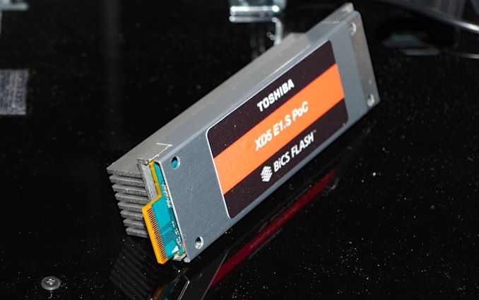
Last year, Marvell announced an NVMe to Ethernet converter that allows an individual NVMe SSD to be connected directly to an Ethernet network, making the SSD accessible through NVMeoF. At first, this converter was demoed on small interposer boards that sit between standard U.2 SSDs and an Ethernet-capable backplane. This year, Marvell and Toshiba showed off a fully integrated Ethernet SSD that adds the Marvell 88SN2400 converter to Toshiba’s existing SSD design. Mechanically, this drive appears to be a 2.5″ U.2 or U.3 SSD, but electrically its host interface is a pair of 25Gb Ethernet links instead of four PCIe lanes.

This year: NVMe to Ethernet converter built-in
These drives have not been formally launched by Toshiba as a shipping product, but they were described as production-ready and were demonstrated in a 24-drive 2U Ethernet JBOF appliance built by Aupera. A typical NVMe JBOF either uses PCIe switches and external PCIe cabling to a few nearby servers, or it contains one or two x86 server CPUs, some PCIe switches from Broadcom or Microsemi and some RDMA-capable Ethernet NICs from Mellanox to provide NVMe over Fabrics functionality. The Ethernet JBOF ditches all of that for one of Marvell’s own Ethernet switch ASICs.

Taking things to the logical next step, Marvell also announced a native Ethernet/NVMeoF SSD controller. The 88SS5000 is effectively their 88SS1098 NVMe controller with the PCIe interface replaced by the dual 25GbE interface used by the NVMe to Ethernet converter. This new single-chip solution for Ethernet-attached SSDs helps cut costs and power consumption, making the whole idea more palatable to datacenter customers. Marvell showed samples of this controller paired with 8TB of Toshiba 96L 3D TLC NAND and 12GB of DDR4 DRAM.

Looking further into the future, Marvell shared their take on the idea of Computational Storage—SSDs that do more than just store data. Marvell is working to integrate a Machine Learning engine into future SSD controllers, allowing inferencing tasks to be offloaded from CPUs or GPUs onto the SSDs that already store the data being processed. The hardware setup is basically the same mess of cables connecting FPGAs to Flash that Marvell has shown in previous years, but on the software side their demo has matured greatly.

In addition to demonstrating realtime object recognition using a pre-trained model, Marvell now has a system to perform offline recognition on videos stored on the SSD. Their demo presented the results of this recognition as a graph showing which objects were recognized over the duration of a video. There was also a content-aware search engine that would return the segments of stored videos that depict the requested objects. For the demo, this functionality was exposed through a simple web interface. In production, the envisioned use case is to have an application server aggregating results from an array of content-aware SSDs that each perform some kind of analytics on their share of the overall dataset.

Source: AnandTech – Marvell at FMS 2019: NVMe Over Fabrics Controllers, AI On SSD
Samsung Display is considering to suspend one of its LCD panel production facilities in South Korea because of oversupply, the company said this week. There is no final decision yet, but falling profitability and lowering demand could trigger the company to halt manufacturing.
LCD panels for various applications including computer displays, televisions, smartphones, digital signage, and other are produced at dozens of factories in China, Japan, South Korea, and other countries creating oversupply and cut-throat competition. Given macroeconomic uncertainties, demand for numerous devices such as TVs is expected to be weak during the year-end shopping season, which puts further pressure on panel makers.
Samsung and other advanced makers have tried to differentiate their own LCD-based products by adding quantum-dot films and other improvements to displays or TVs (to their backlighting, to be more precise), which certainly helped to improve image quality produced by these devices and enabled the manufacturer to charge a premium. Meanwhile, it looks like there are simply way too many LCD panels made these days.
Being the world’s largest maker of LCDs, Samsung operates two giant LCD production facilities in South Korea, as well as one in China. The company naturally wants to keep the latter plant, but the fate of one of the sites in South Korea is something that remains to be seen.
The official statement by Samsung reads as follows:
“Samsung Display has been adjusting the production output and facility operation due to oversupply and worsening profitability, and we are still considering the suspension of the line, but nothing has been decided.”
Samsung’s rival LG Display has converted one of its LCD lines to an OLED plant. In fact, LGD has been focusing on production of OLEDs for quite some time and opened up new OLED sites both in China and in South Korea. Moreover, the company is also considering various scenarios for its remaining LCD facility in South Korea, according to a claim made by its CFO last month.
Related Reading:
Source: Reuters
Source: AnandTech – Samsung Mulls Suspending South Korea LCD Plant Due to Oversupply
What began as Intel’s Ruler concept for a new SSD form factor blossomed into the Enterprise and Datacenter Small Form Factor family of standards, with the version 1.0 specs published in early 2018. Those standards have since been put into production by enough vendors to generate a lot of real-world feedback, and it’s starting to become clear how the numerous options will fare in the long run. At Flash Memory Summit several companies shared their experiences with the new form factors and explained the motivation behind the changes that have been made to the original EDSFF specs.
EDSFF 3″ module next to non-standard 2.5″ drive with EDSFF connector
The 3″ EDSFF form factors (two lengths and two thicknesses) are the most similar to the existing 2.5″ drive form factor, and can be accommodated without overhauling a server’s layout. These 3″ form factors also seem to be attracting the least interest, and if they see widespread use it will primarily be in more traditional enterprise 2U or 3U server applications where they can take the place of U.2 drives and also replace some uses for PCIe add-in cards. The SFF-TA-1008 spec for the 3″ form factors is still sitting at version 1.0, published in March 2018. The most interesting EDSFF 3″ device we ran across at FMS this year was a Gen-Z DDR4 memory module.
Hyperscalers are much more interested in the benefits of the 1U form factors. The EDSFF 1U Long (abbreviated E1.L) form factor is most similar to Intel’s original Ruler concept, and seems best suited for high-density storage. For example, Microsoft Azure is using the 18mm thick E1.L form factor in their Olympus FX-16 1U JBOF, with 16 drives of 16TB each (256TB total) in a 1U OCP chassis that also has PCIe cabling on the front panel. This is pretty much the least dense use case for E1.L drives—the thinner 9.5mm version of E1.L almost doubles the density, at the cost of making cooling more of a challenge.
E1.S bare PCB
The EDSFF 1U Short (E1.S) form factor is shaping up to be more of a general-purpose standard, and has seen the most changes. E1.S was originally conceived as a fairly direct replacement for M.2 that addresses the most important shortcomings of M.2 for datacenter usage: E1.S is a bit wider so that two rows of NAND flash packages can fit on the PCB, it’s hot-swappable, and it can accommodate higher power levels thanks to a 12V supply and easier cooling. (This is also the basic summary for Samsung’s competing NF1 form factor.) The E1.S spec originally defined just the PCB dimensions, leaving it up to the vendor to design an appropriate carrier tray or case. In this bare PCB configuration, the maximum power draw was specified as 12W.
E1.S with heatspreader
Demand for even higher power use cases has resulted in the definition of standard case and heatsink sizes for E1.S. For cards up to 20W, a 9.5mm thick symmetrical case/heatspreader can be used, making E1.S much more like a shortened version of the fully-enclosed E1.L. For even higher power applications, an asymmetrical case with heatsink has been designed, bringing the thickness all the way up to 25mm and allowing for 25W. The 9.5mm symmetrical case will be adequate for most SSD use cases. The 25mm asymmetrical case+heatsink is intended more for non-SSD devices such as accelerators that dissipate most of their power from a single large chip. These new options allow E1.S to support the same power (and performance) levels possible with 2.5″ U.2 drives, while being significantly easier to cool.
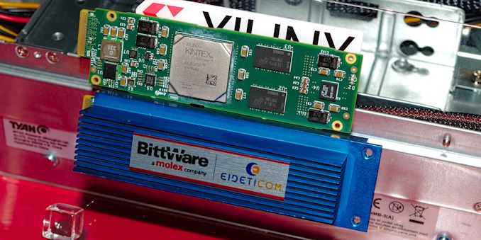
E1.S FPGA Accelerator bare PCB and full case+heatsink
To accommodate these high-power devices, the E1.S form factor now also allows for 8 PCIe lanes using one of the longer connector variants that was already permitted for E1.L and the 3″ form factors. Several vendors at Flash Memory Summit were showing off devices using the E1.S form factor with the asymmetrical heatsink: a mix of SSDs and accelerators.
Source: AnandTech – FMS 2019: EDSFF Form Factors Update – Long, Short, & Everything In-Between

Today NVIDIA announced their earnings for the second quarter of their 2020 fiscal year, which ended on July 28. NVIDIA made tremendous gains during the cryptocurrency boom, and as we saw in Q1, the company has had to deal with the loss of the crypto sales which contributed a lot of revenue to their bottom line in the last year or two. Revenue for Q2 2020 came in at $2.579 billion, which is down 17% from a year ago, and while gross margin was also down 350 bps, it was still a healthy 59.8%. Operating income for the quarter was down 51% to $571 million, and net income was down 50% to $552 million. This resulted in earnings-per-share coming in at $0.90, down 49% from a year ago.
| NVIDIA Q2 2020 Financial Results (GAAP) | |||||
| Q2’2020 | Q1’2020 | Q2’2019 | Q/Q | Y/Y | |
| Revenue | $2579M | $2220M | $3123M | +16% | -17% |
| Gross Margin | 59.8% | 58.4% | 63.3% | +1.4% | -3.5% |
| Operating Income | $571M | $358M | $1157M | +59% | -51% |
| Net Income | $552M | $394M | $1101M | +40% | -50% |
| EPS | $0.90 | $0.64 | $1.76 | +41% | -49% |
Over the last couple of years, NVIDIA has diversified its portfolio, but even so, Gaming continues to be the largest revenue generator at NVIDIA, and by a wide margin. Despite gaming revenue dropping nearly $500 million from a year ago, gaming still accounts for over 50% of NVIDIA’s total revenue. For Q2, gaming brought in $1.313 billion, down from $1.805 billion a year ago. It’s a big drop, but NVIDIA did make gains over Q1 where the drop was 39% year-over-year, compared to the current quarter which had a 27% drop year-over-year. NVIDIA stated that gaming desktop GPU sales fell, which isn’t a surprise considering the crypto craze a year ago, but sales were partially offset by increased notebook GPU sales.
Professional Visualization, which is NVIDIA’s Quadro lineup, had revenue of $291 million for the quarter, which is up 4% from a year ago. As with the gaming segment, increased sales of notebook versions of Quadro were the reason for the increase.
Data Center also had a drop, with revenues coming in at $655 million, which is down 14% from a year ago. NVIDIA saw a large jump in data center GPU sales for AI over the last couple of years, but that growth has stagnated and now regressed. NVIDIA attributes the drop to lower hyperscale revenue, and NVIDIA has started to see some fierce competition in the hyperscale space with companies even creating their own custom silicon for specific workloads. It’ll be interesting to see how NVIDIA responds.
Automotive, which is the market NVIDIA moved their Tegra processor into when they dropped their mobile efforts, continues to do well. Revenue for automotive was a record $209 million, up 30% from a year ago. NVIDIA has made a lot of gains in AI cockpit solutions and autonomous driving solutions, and attributes the revenue gain to a development services agreement they signed in this quarter.
Finally, OEM and Other revenue was $111 million, down 4% from a year ago.
| NVIDIA Quarterly Revenue Comparison (GAAP) ($ in millions) |
|||||
| In millions | Q2’2020 | Q1’2020 | Q2’2019 | Q/Q | Y/Y |
| Gaming | $1313 | $1055 | $1805 | +24% | -27% |
| Professional Visualization | $291 | $266 | $281 | +9% | +4% |
| Datacenter | $655 | $634 | $760 | +3% | -14% |
| Automotive | $209 | $166 | $161 | +26% | +30% |
| OEM & IP | $111 | $99 | $116 | +12% | -4% |
Looking ahead to Q3, NVIDIA is expecting revenues around $2.9 billion, plus or minus 2%. Q3 FY 2019 NVIDIA had revenues of $3.2 billion, so NVIDIA is still expecting to be below those numbers, but edging closer to where they were a year ago.
Source: NVIDIA Investor Relations
Source: AnandTech – NVIDIA Q2 FY 2020 Earnings Report: Continuing Crypto Disruption

Following its decision to focus on specialized process technologies last August, GlobalFoundries has been consolidating its assets as well as selling off businesses and facilities that are not essential for its current strategy. To that end, this week the company announced that it had entered into an agreement to sell off its Fab 9’s photomask operations and IP to Toppan Photomasks. The latter will, in turn, provide photomask production services to GlobalFoundries in the coming years.
Under the terms of the agreement, Toppan Photomasks, a division of Toppan Printing Co., will acquire certain assets of GlobalFoundries’ photomask facility in Burlington, Vermont. The tools and technologies from the Fab 9 will be transferred to Advanced Mask Technology Center (AMTC), a joint venture between Toppan Photomasks and GlobalFoundries in Dresden, Germany; Toppan’s facility in Round Rock, Texas; and other locations the company owns worldwide.
Transfer of the photomask production equipment will enable GlobalFoundries to consolidate its Fab 9 floor space and potentially expand capacity available for production using specialized RF process technologies on 200-mm wafers. The contract maker of semiconductors claims that the transfer of photomask operations from the fab will have no impact on jobs and it will not fire any personnel.
In addition, the two companies announced a multi-year supply agreement in which Toppan will provide photomasks and related services to GlobalFoundries in the USA. Meanwhile, the chipmaker will continue to use AMTC in Dresden. In fact, the latter will gain capacity because of the new tools and will stenghten its positions in Europe.
Related Reading:
Source: AnandTech – GlobalFoundries Sells Off Photomask Assets to Toppan
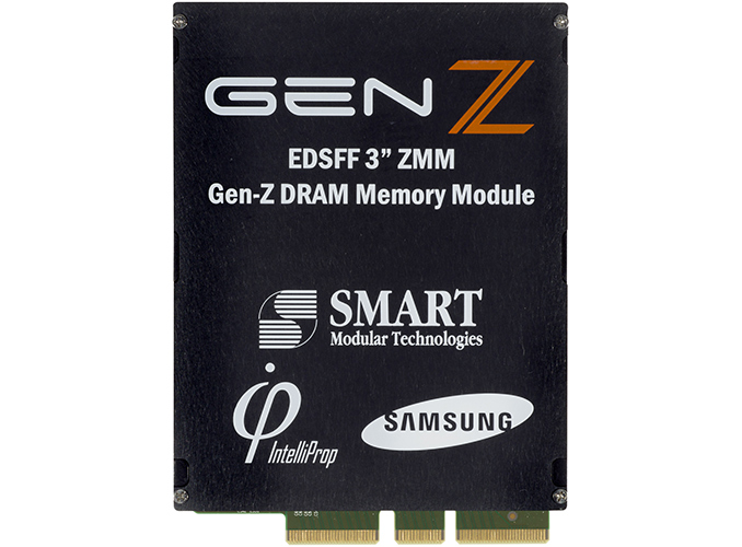
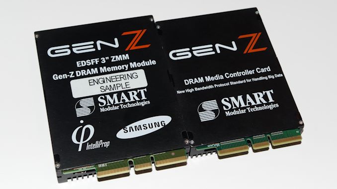
SMART Modular this month demonstrated one of the industry’s first prototypes of a EDSFF 3-inch DDR4 Gen-Z memory module. The ZMM supports advanced functionality enabled by the new interface and offers throughput akin to that offered by today’s DDR4-4000 memory modules.
SMART Modular’s 256 GB ZMM uses Samsung’s 32 Gb 4-high DDR4 DRAM devices as well as IntelliProp’s Gen-Z Mamba memory controller ASSP, which supports multiple access semantics, including byte and block addressable DRAM access, in-band configuration, and access key/region key memory isolation opcodes in a bid to simplify memory access needed to handle emerging data-centric workloads. The controller features 16 Gen-Z lanes with 25 Gbps PHY as well as 400 Gbps aggregate performance. The chip requires up to 20 W of power, so it needs proper cooling.
The Gen-Z module from SMART Module comes in SNIA’s 3-inch 4C SFF-TA-1008/9 form-factor, and offers a 30 GB/s bandwidth along with 400 ns deterministic access latency.
The 256 GB ZMM was demonstrated in rack servers designed by Dell and Hewlett Packard Enterprise specifically to test Gen-Z interconnection.
The showcase of a 256 GB Gen-Z ZMM by a well-known supplier of memory and storage solutions with two makers of servers indicates that the industry is getting ready for a roll-out of Gen-Z products in the future. What remains to be seen is when exactly SMART Modular and its partners will be ready with commercial Gen-Z modules and platforms.
Related Reading:
Source: SMART Modular
Source: AnandTech – SMART Modular Shows Off 256 GB Gen-Z Memory Module

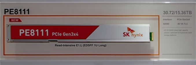
Coming off of the heels of last week’s Flash Memory Summit, today a familiar entity is throwing its hat back into the ring for retail SSDs: SK Hynix. This morning the company is announcing a new line of SSDs, the SuperCore series, which will be sold directly at retail. Kicking off the family will be the Gold S31, a 2.5-inch SATA drive with capacities ranging from 250GB to 1TB.
At a high level, the retail SSD market has remained an odd hodge-podge of collection of vendors. Many first party NAND manufacturers, such as Samsung, Intel, and Toshiba, all produce their own drives in-house for the consumer market. And, for a time, this included SK Hynix as well, who produced and sold their Canvas series of drives. However, the drives were never officially released in North America, and while they can still be found on the grey market, SK Hynix’s retail ambitions have fallen by the wayside as they’ve remained more focused on selling raw NAND and OEM drives.
But after essentially being absent from the retail market for the last couple of years, SK Hynix is going to be re-entering it with some new consumer SSDs. Leading off SK Hynix’s revised consumer lineup is their Gold S31 SSD. This is a 2.5-inch SATA SSD, which is based on SK Hynix’s own NAND and SSD controller.
Unfortunately, SK Hynix isn’t going into a lot of detail about the drive here, so we don’t know which generation NAND and controller they’re using. However there’s a very good chance that this is a retail version of one of their recent OEM drives, as there’s little need to develop a new drive for the retail market, especially the already-overstuffed market for 2.5-inch SATA drives.
| SK Hynix Gold S31 Specifications | ||||
| Capacity | 250 GB | 500 GB | 1 TB | |
| Form Factors | 2.5″ | 2.5″ | 2.5″ | |
| Controller | “SK Hynix Controller” | |||
| NAND | SK Hynix 3D NAND | |||
| Sequential Read | 560 MB/s | |||
| Sequential Write | 525 MB/s | |||
| Endurance | ? | ? | 600 TB | |
| Warranty | Five years | |||
| MSRP | $49.99 | $77.99 | $123.99 | |
What little we do know is that the drives will come in 250GB, 500GB, and 1TB capacities. And with the SATA interface bottlenecking performance, SK Hynix’s 560MB/sec read and 525MB/sec write speeds are right up there with pretty much every other major SATA SSD. Meanwhile, not listed in the company’s official press release but tucked into the retail listings, these confirm that the drives have DRAM, so the Gold S31 drives appear to be aimed at the mainstream market rather than the budget market and the DRAMless drives that are typically found there.
Moving down the spec list, the retail listings for the drive also confirm that the 1TB model is rated for 600 TB Written. Spreading this out over the drive’s 5-year warranty period, we end up with 0.3 drive writes per day, both of which are comparable to arch-rival Samsung’s EVO drives.

All told, while SK Hynix is reentering the retail market, they are still doing so in a fairly conservative manner. The company is starting things off by selling their drives exclusively in North America through Amazon, with plans to expand into Europe and widen their distribution network next year. The company has also mentioned that they’ll have a PCIe drive next year as well, though they aren’t offering any further information on that drive at this time.
Finally, taking a look at pricing, all 3 Gold S31 drives are already available on Amazon. With the 250GB drive starting at $50 and reaching $124 for the 1TB drive, SK Hynix has launched the drives at a small premium over other mainstream SATA drives. Ultimately, I suspect the company is looking to get some value for its brand name, but given just how competitive and oversaturated the SATA SSD market is, making a dent in the market without joining the race to the bottom in drive prices is going to be difficult task.
Source: AnandTech – SK Hynix Re-Enters Retail SSD Market, Launches Gold S31 SATA Drives

Huawei’s Mate X garnered quite of attention at Mobile World Congress earlier this year as one of the industry’s first foldable 5G smartphones. Unfortunately for those looking to get one of such handsets, it will only be available in the fourth quarter, months later than expected originally.
Featuring an 8-inch foldable display with a 2480×2200 resolution and an 8:7 aspect ratio, the Huawei Mate X was expected to be released in the middle of 2019. At some point, its launch was postponed to September and recently the company said that it would be available only in November, reports TechRadar. The delay will likely be the last one as the company is looking forward to start selling its flagship 5G device ahead of the holiday sales season in Europe and the US.
After visiting Huawei’s headquarters earlier this month, TechRadar reports that the company had to slightly redesigned the Mate X from what was shown at MWC: the device now has a slightly different ‘Falcon Hinge’ and a slimmer lock button.
The reasons why Huawei had to delay the launch of its Mate X from mid-2019 to November are not completely clear. Obviously, the aforementioned redesigns took time to implement and test. Meanwhile, Huawei faced uncertainties with its partners like like Google after it was added to the US Entity List in May. Considering the fact that we are talking about a smartphone that is going to cost $2000, the company is naturally interested in getting the product to market without any compromises or glitches.
Related Reading:
Source: TechRadar
Source: AnandTech – Huawei Delays Launch of Foldable Mate X to Q4

For many PC enthusiasts, overclocking means a lot of fun, both in terms of process and the end result. To a large degree overclocking is a lottery that is never guaranteed, and when it comes to AMD’s latest Ryzen 3000 processors, getting a CPU with high overclocking potential is not easy at the moment. This has left an opening in the market for retailers who are selling pre-binned chips with guaranteed overclocking potential.
There are several stores that sell pre-binned CPUs and other components: Silicon Lottery from Texas, USA; Caseking from Germany; and Overclockers UK. Silicon Lottery was the first company to start offering pre-binned AMD Ryzen 3900X processors last month and by now their entire first batch has been sold. Meanwhile, this week Caseking began to sell AMD’s latest CPUs with a guaranteed overclocking potential.
The list of pre-binned AMD’s Ryzen 3000-series processors to be available from Caseking includes Ryzen 9 3900X, Ryzen 7 3700X, and Ryzen 5 3600, but at present only the model 3700X is available. All the CPUs are pretested by Roman “der8auer” Hartung, a well-known overclocker, using Prime95 26.6 software with an FFT length of 1344 for at least one hour with AMD’s Wraith Prism cooler. Meanwhile, voltage of the chips is kept under 1.4 V.
| Pre-Binned AMD Ryzen 3000 CPUs by CaseKing.de | ||||||||
| Cores/ Threads |
Default Clocks Base/Boost |
Guaranteed OC (base) | L3 | TDP (default) |
Price (EUR) |
|||
| Ryzen 9 3900X | 12/24 | 3.8/4.6 GHz | 4.3 GHz | 64 MB | 105 W | €619 | ||
| 4.25 GHz | €599 | |||||||
| 4.2 GHz | €579 | |||||||
| Ryzen 7 3700X | 8/16 | 3.6/4.4 GHz | 4.3 GHz | 32 MB | 65 W | €449 | ||
| 4.25 GHz | €429 | |||||||
| 4.20 GHz | €399 | |||||||
| Ryzen 5 3600 | 6/12 | 3.6/4.2 GHz | 4.3 GHz | 32 MB | 65 W | €300 | ||
| 4.25 GHz | €280 | |||||||
| 4.2 GHz | €260 | |||||||
Pre-binned processors from Caseking cost €50 – €100 more than regular models, so overclocking in this case is not a ‘free’ performance upgrade. Furthermore, buyers in Germany have to pay VAT of 19%. The good news, however, is that as per European laws, the CPUs are backed with a two-year warranty.
Related Reading:
Sources: Caseking, Tom’s Hardware
Source: AnandTech – Retailers Begin to Sell Pre-Binned AMD Ryzen 3000 CPUs