Top 10 Foundries See Revenue Drop Nearly 15% Year-over-Year

The top 10 contract makers of chips saw their Q1 2023 revenue decline by 14.6% year-over-year and 18.6% quarter-over-quarter, according to the most recent report by TrendForce. The market intelligence firm attributes falling sales of foundries to ongoing sluggish demand in the end-market demand and seasonality. TSMC and Samsung Foundry retained top positions, whereas GlobalFoundries is back to No. 3, surpassing UMC for the first time in a while.


The world’s 10 largest foundries earned $27.3 billion in Q1 2023, a 14.6% drop year-over-year (YoY) and an 18.6% drop quarter-over-quarter (QoQ), based on TrendForce data. The revenue decrease resulted from a weakened demand for mass-market applications that use leading-edge fabrication technologies, such as client PCs and smartphones, and was particularly noticeable at TSMC and Samsung Foundry. Meanwhile, UMC and DB Hitek suffered even more than TSMC.


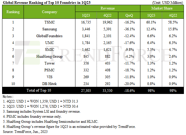
TSMC, the world’s largest contract maker of chips with a 60.1% revenue share, earned $16.74 billion, reflecting a 16.2% decrease from the previous quarter and a 4.5% decline from the same period last year. Soft demand for client PCs and smartphones caused lower utilization of TSMC’s N7 (7 nm-class) and N5 (5 nm-class) process technologies, according to TrendForce. Consequently, TSMC’s revenue attributed to its N7 family of production nodes decreased by 20%, whereas the foundry’s earnings from its N5 lineup of fabrication technologies declined by 17%. 


TrendForce believes that although urgent orders in the second quarter may provide a brief relief for TSMC, their facilities’ enduringly low usage rate suggests that the earnings will keep dropping, though more gradually than in the first quarter. TSMC expects its Q2 earnings to be below those in Q1, mainly due to seasonality and market uncertainties.


Samsung Foundry suffered dropping utilization both for 200-mm and 300-mm fabs, resulting in a 36.1% QoQ and 35.25% YoY plunge in Q1 revenue, the highest in the industry, bringing it down to $3.45 billion, according to TrendForce. The market researchers now expect Samsung Foundry to land additional occasional orders for specific components in Q2. Still, these orders are expected to be fueled by brief inventory restocking and may not necessarily indicate a resurgence in end-market demand. Also, TrendForce believes that increasing orders for SF3E (3 nm-class) chips will also be a revenue driver for Samsung’s contract chipmaking division.  


GlobalFoundries‘s in Q1 2023 totaled $1.84 billion, reflecting a 12.4% reduction from the previous quarter and a 5.2% drop from the same quarter a year ago. GlobalFoundries focuses on specialized process technologies and serves sectors like automotive, aerospace, defense, IoT, and industrial, where demand is relatively stable. This sustained stability has enabled GlobalFoundries to overtake UMC, securing the third spot in revenue rankings in Q1. As for Q2 projections, GF anticipates benefiting from steady orders and maintaining capacity usage, thus keeping revenue at par with the first quarter.


UMC earned $1.78 billion in Q1 2023, a 17.6% sequential drop and a 21.4% decline year-over-year. TrendForce claims that this decrease was especially apparent in the 28/22 nm and 40 nm processes, each falling by a minimum of 20%. The company anticipates the utilization rate of its 200-mm fabs to drop below 60% in the second quarter of 2023 due to fewer customer orders for PMICs and MCUs. By contrast, the 300-mm fab utilization rate is set to benefit from immediate orders for 28/22 nm products like TV SoCs and LCD panel timing controllers, leading to an anticipated 80% utilization rate. Given the steady ASP, UMC predicts its revenue will either maintain the current level or see a slight uptick in the upcoming quarter.


SMIC‘s Q1 2023 revenue reached $1.46 billion, a 9.8% decrease from the previous quarter and a 20.8% decline from Q1 2022. The interesting part is that while demand for the foundry’s 300-mm wafer processing services remained stable and increased by 1% – 2%, the company’s revenue attributed to 200-mm fabs plummeted by 30% QoQ, according to TrendForce. The analysts believe that steady 300-mm orders were driven by a diverse product portfolio and backing from local demand in China. TrendForce projects that SMIC will continue to benefit from increased orders for products like Driver ICs and NOR Flash and maintain advantages from China’s demand.


TrendForce predicts that the revenue of the Top 10 foundries will drop further in Q2 2023. Although supply chains are expected to build inventory gradually in response to peak season demand in H2 2023, the slow consumption and inventory accumulation have led to more cautious stockpiling. As a result, the market intelligence firm predicts a relatively stable Q2 for foundries with only modest increases in capacity utilization rates. Yet, some rush orders for products like TV SoCs, WiFi 6/6E, and TDDI can noticeably increase the utilization of fabs.


Source: TrendForce


Source: AnandTech – Top 10 Foundries See Revenue Drop Nearly 15% Year-over-Year

AMD Ryzen Pro 7000 and 7040 Series Processors : Zen 4 For Commercial Deployments

As is a constant whenever AMD launches their latest desktop and mobile processors, they typically deploy and release a professional and commercial line-up of these processors a few months later. For the desktop and mobile (server/workstation is Threadripper Pro), the latest Ryzen Pro 7000 for desktop and Ryzen Pro 7040 HS and 7040 U series for mobile builds upon the consumer range by adding several ‘Pro’ based features that add layers of additional security and remote manageability that sets them apart from their more consumer-focused silicon siblings.


On top of the advantages of adding Zen 4 cores to enhance performance and efficiency compared to their previous Ryzen Pro with Zen3+ portfolio, selected AMD’s Ryzen Pro 7040 series SKUs will include their latest Ryzen AI block integrated within the silicon to bolster capabilities when using specific AI-focused workloads. AMD has three Ryzen Pro 7000 series processors for desktops, including one 6C/12T, 8C/16T, and 12C/24T trio of Pro-enabled SKUs, as well as three Ryzen Pro 7040HS models and three lower powered Ryzen Pro 7040U series SKUs to select from.


Source: AnandTech – AMD Ryzen Pro 7000 and 7040 Series Processors : Zen 4 For Commercial Deployments

Microsoft to Bring Game Pass Games to NVIDIA's GeForce Now

Microsoft on Sunday announced plans to bring select PC Game Pass games to NVIDIA’s GeForce Now cloud streaming service later in 2023. The move will allow gamers to enjoy Microsoft’s curated collection of PC games on high-end hardware in the cloud without purchasing either the games or a high-end gaming device (PC, Xbox), all for a monthly fee. 


“Game Pass members will soon be able to stream select PC games from the library through NVIDIA GeForce Now,” wrote Joe Skrebels, Xbox Wire Editor-in-Chief, in a blog post. “This will enable the PC Game Pass catalog to be played on any device that GeForce Now streams to, like low-spec PCs, Macs, Chromebooks, mobile devices, TVs, and more, and we will be rolling this out in the months ahead.”


NVIDIA’s GeForce Now is a cloud gaming service known for offering cutting-edge gaming hardware, including the highly acclaimed GeForce RTX 4080 graphics card that is offered in the top tier subscription ($19.99 per month) aimed at demanding gamers. Meanwhile, Microsoft’s PC Game Pass subscription ($9.99 per month) gives access to over 100 titles of different genres and a library of Electronic Arts games. The value proposition of Game Pass on GeForce Now is evident as it allows to play high-quality PC games on an advanced rig for $30 a month, or $360 a year, which is considerably cheaper than buying a gaming PC.


There are a couple of things to keep in mind though. Microsoft has only confirmed that a “selected range” of Game Pass PC games will be compatible with GeForce Now. Also, the question of whether EA Play games will be supported is yet to be clarified. Thus, it remains uncertain how many games from Microsoft’s subscription will eventually be compatible with the GeForce Now platform.


Furthermore, cloud game streaming comes with its own quirks, such as longer loading times and increased latencies, so its overall experience is not exactly the same as that provided by a local gaming PC with a high-end CPU and a GeForce RTX 4080 graphics board. Still, NVIDIA’s GeForce Now with the GeForce RTX 4080 tier provided better experience than Microsoft’s Xbox Cloud Gaming service, offering higher performance and lower latency, according to a comparison by The Verge.


Bringing PC Game Pass games to NVIDIA’s GeForce Now platform — which currently supports Epic’s Game Store and Valve’s Steam — could potentially enhance the appeal of both services for gamers. Meanwhile, some might perceive this move as a strategic effort to pacify regulators in light of Microsoft’s ongoing acquisition of Activision Blizzard. In general, the move shows that the software giant is willing to distribute its services and games on platforms beyond Windows and Xbox.


In separate news, Microsoft introduced a new, larger capacity version of its Xbox Series S console. The all-black Xbox comes with a 1 TB SSD – up from 512GB on the base model – and carries a $50 price premium, putting the final price tag at $349. The new system will be available starting September 1, 2023.


Source: AnandTech – Microsoft to Bring Game Pass Games to NVIDIA’s GeForce Now

Western Digital Estimates HAMR HDDs to Emerge in 1.5 Years

Western Digital is somewhat behind its rival Seagate in adopting heat-assisted magnetic recording (HAMR), which promises radical improvements to areal density and HDD capacities. Still, the company expects hard drives that use this recording method to enter mass production in the next 1.5 years. This technology will open doors for nearline drives offering 40 TB – 50 TB capacities in the coming years.


Seagate recently said it was months away from introducing its 32 TB nearline hard drives featuring its HAMR technology, with 36 TB and 40 TB HDDs to follow. The introduction of 32 TB hard drives will undoubtedly put Seagate in a leading position as far as capacity is concerned, as the highest capacity drive that Western Digital has today is its Ultrastar DC HC670 26 TB featuring UltraSMR set of technologies. At a recent conference, financial analysts asked Western Digital when the company expects its HAMR HDDs to emerge. The firm envisions these drives to enter mass production in circa 1.5 years.


“On the HAMR side, we are probably one year to 1.5 years plus before we get sort of volume production anyway,” said Wissam Jabre, the chief financial officer of Western Digital, at the Bank of America Securities 2023 Global Technology Conference (via SeekingAlpha).


HAMR is a highly complex technology. It requires novel platters capable of enduring intense local heat of approximately 450°C or higher (generated using a laser with an ~810 nm wavelength and a ~20 mW power) without deforming over time. These platters are expected to be made from glass substrates and covered with a thin Fe-Pt alloy magnetic layer to ensure reliability and resist eventual deformation.


“HAMR could be one of the next on the roadmap,” said Jabre. “[…] Our engineering teams have done a lot of R&D around [HAMR] […], it requires a lot of work on the material science as well as the physics. But also, much work is required in terms of commercialization, meaning being able to manufacture at scale, ensuring the yields are where they need to be, and having a reliable product that can last for several years. So, it takes time to get there.”


All HDD makers have been working on HAMR HDDs for well over a decade, but only Seagate decided to bet on HAMR boldly. In contrast, Toshiba and Western Digital adopted energy-assisted perpendicular magnetic recording (ePMR) and microwave-assisted magnetic recording (MAMR) before adopting HAMR.


Western Digital’s roadmap includes the 2nd Generation ePMR 2 platform, which allows for areal densities over 1.3 Tb/inch2 (an 18% over ePMR). Such areal density will enable the company to build 3.5-inch platters with a capacity of over 3.5 TB. Thus Western Digital will be able to offer HDDs with a ~36 TB capacity featuring 10 of such disks in the coming quarters. Meanwhile, the company says this technology will be used for CMR HDDs with 24 TB – 30+ TB capacity points.


Of course, the key question is when precisely such drives are set to be announced, qualified, and shipped. But at least it looks like Western Digital is set to stay competitive with Seagate regarding HDD capacities for the foreseeable future.


As for HAMR, Western Digital expects this recording technology to enable areal densities higher than 2 Tb/inch2, which allows it to build ~5.4 TB 3.5-inch platters, opening doors for HDDs with capacities of around 50+ TB.


Source: AnandTech – Western Digital Estimates HAMR HDDs to Emerge in 1.5 Years

TSMC Opens Advanced Backend Packaging Fab for AI and HPC Products

TSMC on Friday formally opened its Advanced Backend Fab 6 facility, which it will be using to expand the company’s capacity for building high-end, multi-chiplet products. The facility is said to be the first all-in-one automated fab offering 3DFabric integration of front-end to back-end process and testing services.


TSMC’s Advanced Backend Fab 6 can process about one million 300-mm wafers per year as well as more than 10 million hours of testing per year. The factory occupies 14.3 hectares in Zhunan Science Park and has a cleanroom that is larger than the combined cleanroom spaces of all other TSMC advanced backend fabs, making it TSMC’s biggest advanced packaging facility to date, according to the company.


TSMC said that its Advanced Backend Fab 6 is ready for mass production of TSMC-SoIC (System on Integrated Chips) process technology, which includes such frontend 3D stacking techniques as chip-on-wafer (CoW) and wafer-on-wafer (WoW). The fab is also designed to handle advanced backend packaging technologies, such as integrated fan-out (InFO) and chip-on-wafer-on-substrate (CoWoS) that are used for chips like Apple’s M2 Ultra, AMD’s Instinct MI300, and NVIDIA’s A100 and H100.


“Chiplet stacking is a key technology for improving chip performance and cost-effectiveness. In response to the strong market demand for 3D IC, TSMC has completed early deployment of advanced packaging and silicon stacking technology production capacity, and offers technology leadership through the 3DFabric platform,” said Dr. Jun He Vice President, Operations / Advanced Packaging Technology & Service, and Quality & Reliability.


Perhaps the most notable feature of TSMC’s Advanced Backend Fab 6 is comprehensive five-in-one intelligent automated material handling system that spans over 32 kilometers. The production information, starting from the wafer stage to the die, is integrated with dispatching systems to speed up the manufacturing cycle. This process is augmented with AI to carry out precise process control and real-time defect detection to maximize yields. This is particularly important as when you package a multi-chiplet solution like AMD’s MI300 any abnormality on the package level immediately invalidates all the chiplets that are on it causing a loss that costs at least thousands of dollars. The fab’s data processing capability per second is 500 times that of a typical front-end fab, which enables a thorough production history for each die and allows the foundry to trace each die it processes at the fab.


“With the production capacity that meets our customers’ needs, we will unleash innovation together and become an important partner that customers trust in the long term,” added Jun He.


Source: AnandTech – TSMC Opens Advanced Backend Packaging Fab for AI and HPC Products

The AlphaCool Core Storm XT45 & Core Hurrican XT45 Liquid Cooling Kits Review

As summer kicks off in the Northern Hemisphere, today we’re bringing the water to our PC cooling testbed with a look at a pair of kits from AlphaCool’s range of ready-to-install liquid cooling sets. Specializing in liquid cooling, the German firm offers a complete range of liquid cooling parts – from radiators and reservoirs to tubes and connectors – both on an individual basis and as part of complete cooling kits. These kits essentially are collections of individual parts that are conveniently packed together, saving the trouble of picking items one by one and getting everything needed for a CPU liquid cooler at a small discount.


For today’s review, we’re looking at two of the three series of kits that AlphaCool currently offers, the Core Storm XT45 240 mm and the Core Hurrican XT45 360 mm. Paired with 240 mm and 360 mm radiators respectively, the two kits are largely similar in scope as high-end open loop water cooling sets. However the Hurrican kit, besides offering more cooling headroom overall via its larger radiator, diverges from its Storm coutnerpart by using hard, molded tubing. The end result is a very different building experience, even if the underlying physics at play are much the same.


Source: AnandTech – The AlphaCool Core Storm XT45 & Core Hurrican XT45 Liquid Cooling Kits Review

Cooler Master Introduces MasterAir MA824 Stealth 250W Dual-Tower CPU Cooler

Cooler Master has strengthened the brand’s already prolific CPU air cooler portfolio with the latest addition in the form of the MasterAir MA824 Stealth. There’s also a 30th-anniversary edition of the new cooler with an ARGB fan. The MasterAir series is already home to some of the more prominent high-performance CPU coolers; therefore, the MasterAir MA824 Stealth will fit right in.


The MasterAir MA824 Stealth features a dual-tower design like many popular CPU air coolers, such as the Cooler Master’s previously-released MasterAir MA624 Stealth or the Noctua NH-D15. Aesthetically-conscious consumers will value the MasterAir MA824 Stealth’s all-black exterior since it helps the CPU cooler blend into most PC builds. The top cover is a nice touch that adds some flair to the design. Checking in with the dimensions of 6.4 x 5.9 x 6.5 inches (162.2 x 150.6 x 165.6 mm), the MasterAir MA824 Stealth is significantly larger than the MasterAir MA624 Stealth (5.7 x 6 x 6.3 inches) but falls in the same ballpark as the Noctua NH-D15 (6.3 x 5.9 x 6.5 inches).


Cooler Master MasterAir MA824 Stealth 250W
Type Dual Tower Cooler
Dimensions 162.2 x 150.6 x 165.6 mm
Fans 1 x 135mm “Mobius” Fan, 63.1 CFM

1 x 120mm “Mobius” Fan, 63.6 CFM
RGB Yes (Anniversary Edition)
Supported Sockets Intel: LGA1700, LGA1200, LGA1151, LGA1150, LGA1156, LGA1155


AMD: AM5, AM4
Warranty 5 Years
Price £99.99


Featuring a nickel-plated copper base that makes direct contact with the processor, the MasterAir MA824 Stealth transfers heat to the dual-tower heatsinks through eight composite copper heat pipes. The cooler has two more heat pipes than the prior MasterAir MA624 Stealth and the Noctua NH-D15. Cooler Master revised the fin stack design and thickness on the MasterAir MA824 Stealth compared to the MasterAir MA624 Stealth to improve thermal performance. Cooler Master had displayed the MasterAir MA824 Stealth at Computex 2023, where the cooler featured a coating that reacts to the temperature. Basically, the heat pipes and heatsink would turn red when heat dissipation is in action. It’s a shame that the cool feature didn’t make it to the retail product.


Despite the large heatsinks, the MasterAir MA824 is compatible with tall memory modules. With its default configuration, there are 1.7 inches of clearance space and up to 2.6 inches in a single-fan setup. The MasterAir MA824 is more generous than the Noctua NH-D15, which provides 1.3 and 2.5 inches of clearance in default and single-fan mode, respectively. The MasterAir MA824 Stealth is compatible with many recent and old sockets. It supports LGA1700, LGA1200, and LGA115x from Intel and the AM4 and AM5 sockets.


Cooler Master equips the MasterAir MA824 Stealth with two Mobius cooling fans with loop dynamic bearings. The vendor placed the pair of PWM cooling fans in a staggered design to maximize push-pull performance. Consumers can add a third fan of their choice. The middle fan is a Mobius 135 (135mm) that delivers up to 1.92 mmH₂O of static pressure with a maximum noise level of 24.6 dB(A), whereas the other is the Mobiius 120 (120mm), which is rated for 2.69mmH₂O at 22.6 dB(A). On the MasterAir MA824 Stealth 30th Anniversary Edition, the 120mm fan has vibrant ARGB lighting. On paper, Cooler Master’s Mobius fans seemingly perform better than Noctua’s NF-A15 PWM 140mm fans that cool the NH-D15. The NF-A15 PWM fans have a static pressure of 1.51 mmH₂O at 19.2 dB(A). While NF-A15 PWM lacks the performance of the Cooler Master fans, it is substantially more silent during operation. Cooler Master rates the MasterAir MA824 Stealth’s cooling capacity up to 250 watts with the dual-fan layout.


The MasterAir MA824 Stealth comes with a five-year warranty. Cooler Master didn’t reveal the U.S. pricing or availability for the MasterAir MA824 Stealth or MasterAir MA824 Stealth 30th Anniversary Edition. The cooler is already available in the U.K. with a £99.99 (~$125) MSRP.


Source: AnandTech – Cooler Master Introduces MasterAir MA824 Stealth 250W Dual-Tower CPU Cooler

Palm-Sized Minisforum EM680 Desktop PC Packs AMD's Ryzen 7 6800U and USB4

We’ve seen AMD’s Ryzen Mobile 6000 series chips show up in several mini-PC devices thus far, and now a recently-released mini-desktop from Minisforum is the smallest yet. The Mini-PC specialty firm has launched its Mercury EM680, an ultra-compact PC based on AMD’s Ryzen 7 6800U that is pushing the envelope on compute density, using a far more powerful SoC than we tend to see in these daintiest of devices.


In terms of size, the Minisforum Mercury EM680 can literally fit in the palm of a hand and is smaller than a can of Coke. Underneath it all, Minisforum is taking full advantage of the mobile nature of AMD’s recent laptop chips, packing AMD’s Ryzen 7 6800U processor (8C/16T@4.70 GHz, Radeon RX 680M) and related hardware into the tiny desktop PC. To help achieve the PC’s small size, Minisforum is also relying on soldered-down LPDDR5 memory, pairing the AMD SoC with either 16 GB or 32 GB of LPDDR5-6400. And finally, storage is provided by an M.2 2230-sized SSD hooked up to the SoC’s PCIe 4.0 interface.


While the soldered-down memory means there’s no option for further memory expandability, it is relatively easy to replace the M.2 drive with a higher-capacity one. Minisforum is selling SKUs with 512GB and 1TB drives, though 2TB drives are also available these days from third parties, albeit at a premium. External graphics expandability is technically also an option via the USB4 Type-C port – though you won’t find any eGFX boxes nearly as small as the Mercury.


To ensure consistent performance of the APU, memory, and SSD at high loads, the system is equipped with Minisforum’s Cold Wave 2.0 cooling system, which uses heatsinks that remove heat from both sides of the motherboard, heat pipes, and a blower fan. Minisforum notes that the PC supports a silent mode, though the relatively high 28W+ TDP of the 6800U at full throttle means that active cooling is absolutely needed if you want to sustain that kind of performance for any appreciable length of time.


When it comes to connectivity, it looks quite rich, at least as far as miniature systems are concerned, as the system features an onboard Wi-Fi 6E + Bluetooth 5.3 module, two USB4 connectors with DP Alt Mode, three USB 3.2 Gen2 Type-A ports, a TF Card slot, and an HDMI 2.1 output, and a TRRS connector for headsets. Given display output capabilities and AMD’s Radeon RX 680M integrated GPU, the machine can handle three monitors; the USB-C-driven displays will support an 8Kp60 resolution, whereas the HDMI 2.1 can support an up to 4Kp144 output.


As far as actual dimensions are concerned, the Minisforum Mercury EM680 measures 80×80×43 mm — which is around 40% smaller that the company’s typical small form-factor PCs. The system does not have an integrated PSU, but it comes with a small 65W USB Type-C power adapter.


Traditionally, Minisforum’s systems are not that expensive. The cheapest configuration with 16 GB of memory and a 512 GB SSD is priced at $399 (down from $499), whereas the range-topping model with 32 GB of LPDDR5 and a 1 TB drive is priced at $489 (down from $609).


Source: AnandTech – Palm-Sized Minisforum EM680 Desktop PC Packs AMD’s Ryzen 7 6800U and USB4

SK Hynix Starts Production of 238-Layer 3D NAND: 2400 MT/s

SK Hynix announced this week that it had started volume production of its 238-layer TLC NAND memory. The new device promises higher bit density and lower NAND bits cost for the manufacturer and enables ultra-high-performance SSDs as it features a very high interface speed of 2400 MT/s.


SK Hynix’s first 238-layer 3D TLC NAND device has a 512 Gb capacity (64 GB). It has a number of benefits when compared to its 176-layer predecessor, including a 34% higher manufacturing efficiency (i.e., smaller die size, lower usage of materials, and expensive process steps, etc.), a 21% lower power consumption during read operations thanks to the ONFI 5.0 interface with the NV-LPDDR4 signaling method, and a 2400 MT/s interface transfer rate, which is a 50% increase.


The latter is perhaps the most crucial advantage of the new memory chip for PC enthusiasts, as contemporary and upcoming client SSDs with a PCIe 5.0 x4 interface need high-speed memory devices to saturate it. Currently, available 3D NAND with a 1600 MT/s interface can only enable drives with an approximately 10 GB/s sequential read/write speed, but to get to 12.5 GB/s and even higher, one needs to either use high-speed memory or use more memory devices and an appropriate controller. 


SK Hynix’s 238-layer 3D TLC NAND uses string stacking to join a pair of 119-layer decks as well as charge-trap, CMOS under Array (CuA) architecture, which places NAND logic under the 3D NAND memory cells array to reduce die size and costs. This is why SK Hynix calls this architecture 4D NAND.


SK hynix 3D TLC NAND Flash Memory
  238L 176L
Layers 238 176
Decks 2 (x119) 2 (x88)
Die Capacity 512 Gbit 512 Gbit
Die Size (mm2) 35.58mm2 ~47.4mm2
Density (Gbit/mm2) ~14.39 10.8
I/O Speed 2.4 MT/s

(ONFi 5.0)
1.6 MT/s

(ONFI 4.2)
CuA / PuC Yes Yes


SK Hynix is the third major maker of NAND flash memory to start production of 3D NAND with over 200 layers. SK Hynix said that one of the large smartphone makers was about to complete compatibility tests with its 238-layer 3D NAND devices. Once it does, SK Hynix will start shipping these memory chips to the handset producer. Eventually, these devices will be used for PCIe 5.0 SSDs and high-capacity server drives, the company said.


“SK Hynix has developed solution products for smartphones and client SSDs which are used as PC storage devices, adopting the 238-layer NAND technology, and has moved into mass production in May,” a statement by SK Hynix reads. “Given that the company secured world-class competitiveness in price, performance, and quality for both 238-layer NAND and the previous generation 176-layer NAND, we expect these products to drive earnings improvement in the second half of the year.”


Source: SK Hynix


Source: AnandTech – SK Hynix Starts Production of 238-Layer 3D NAND: 2400 MT/s

Big Leap for Hard Drive Capacities: 32 TB HAMR Drives Due Soon, 40TB on Horizon

Offering a brief update on the future of hard drives, Seagate has shared some fresh insights concerning launch of its next generation hard drives featuring its heat-assisted magnetic recording (HAMR) technology. The company’s initial commercial HAMR hard drive is set to offer a 32 TB capacity, presumably in the third quarter of 2023, but the new recording technology will enable a relatively quick capacity increase to 40 TB. Meanwhile, high-capacity HAMR HDDs will co-exist with yet-to-be-released 24 TB and 28 TB drives.


The initial 32 TB HAMR-based HDDs from Seagate will rely on the company’s 10-platter platform that is akin to that already in use by the company and which has predictable yields and which eliminates one potential point of failure. Given that the company will have to use new media and new write heads with its HAMR hard drives, it is a reasonable move to keep re-using as many proven parts as possible. That 10-platter HAMR platform will be used for 36TB, 40TB, and even higher-capacity HDDs going forward, presumably with as few changes as possible.


“When you go to HAMR, our 32TB is based on 10 disks and 20 heads,” said Gianluca Romano, Seagate’s chief financial officer, at the Bank of America 2023 Global Technology Conference (via SeekingAlpha). “The following product will be a 36TB and will still be based on 10 disks and 20 heads. So, all the increase is coming through areal density. The following one, 40TB, still the same 10 disks and 20 heads. Also, the 50TB, we said at our earnings release, in our lab, we are already running individual disk at 5TB.”


Earlier this year Seagate said that it would ‘launch its 30-plus terabyte platform in the June quarter,’ so expect these drives to get into hands and racks of hyperscale cloud service providers in the coming months.


Back in April the company said it was shipping HAMR drives inside its Corvault systems for revenue, however, the company refrained from officially disclosing their capacities and only indicated that they were based on the 30 TB+ platform. Meanwhile the company is shipping its HAMR HDDs for qualification to hyperscalers, which will deploy them after they pass their tests.


In anticipation of the full rollout of HAMR drives, some cloud service providers may opt to use Seagate’s 24TB HDDs, which rely on its traditional perpendicular magnetic recording (PMR) technology with two dimensional magnetic recording (TDMR) read heads. Additionally, some may even go with 28 TB hard drives that use shingled magnetic recording. Meanwhile, Seagate stresses that these HDDs will be its final high-capacity nearline drives that use perpendicular magnetic recording.


“So, we have a 24TB coming out soon, next few months, you will see it,” said Romano. “That is the last PMR product. So I would say [higher] capacity point above 24TB PMR, that is probably 28TB SMR.”


Source: AnandTech – Big Leap for Hard Drive Capacities: 32 TB HAMR Drives Due Soon, 40TB on Horizon

Realtek Accuses MediaTek of Conspiring Against It with Patent Hoarder

This week, Realtek sued rival MediaTek in Northern California federal court, accusing it of conspiring against it with a patent holder in a bid to drive Realtek out of business. Reuters reports that Realtek asserts that MediaTek intends to monopolize the markets of smart TVs and set-top-boxes and asks the court to protect itself from the ongoing injury and the market from unfair competition practices.


It is not a secret that various patent assertion entities (PAE), a juridical term for patent hoarders, acquire patents and then sue different designers for royalties. In 2019, MediaTek entered into a patent license agreement with Future Link and its owner IPValue to license some of the patents issued initially to NXP Semiconductor and Philips. While this would be a reasonably typical license agreement, it contained a secret provision, which included MediaTek’s demanding Future Link act against its rivals, including Realtek. 


Future Link sued Realtek for alleged patent infringement on April 13, 2021, accusing the chip designer of infringing two of its patents related to TV SoCs. By the end of 2021, Future Link reportedly expanded the list of its allegations against Realtek with two more patents and then dropped some of the claims. The important thing here is that Future Link alleges that all of Realtek’s products that use Arm’s AXI interface for multi-core SoCs infringe its patents, which in turn means that virtually all of Realtek’s TV chips use its IP illegally and have to be barred from the market, which will eliminate a rival for Mediatek, which already controls 60% of the TV SoC market, according to Reuters citing the lawsuit.


At the time, Realtek was not aware that the action brought by Future Link was inspired by its rival MediaTek, the company says. 


“In April 2022, there was a shocking revelation regarding that seemingly innocuous agreement,” Realtek states. “Discovery revealed that before the litigation against Realtek began, the license agreement among MediaTek, IPValue, and Future Link included a secret litigation ‘bounty’ provision previously hidden from the public and Realtek. […]. Specific details of this scheme remain hidden from the public even today because Future Link has managed to keep the arrangement buried under confidentiality obligations and protective orders.”


On April 12, 2022, an Administrative Law Judge at the ITC said that the license agreement between Future Link and MediaTek contained a demand for action against Realtek.


“At a minimum, it would seem to warrant an action by Realtek against either Future Link or its counterparty for unfair competition,” the ALJ wrote. 


Realtek says its move aims to counter a modern-day monopolist and its allies to protect itself, uphold competition in the semiconductor industry, and hold the offenders — MediaTek, Future Link, and IPValue — accountable. Any damages recovered by Realtek from this action will be donated to charity.


“Because Realtek seeks to protect the public interest with this action, Realtek will donate the amount of damages that it recovers to charity,” the company said.


MediaTek, Future Link, and IPValue did not comment on the story.


Sources: ReutersReuters (PDF)


Source: AnandTech – Realtek Accuses MediaTek of Conspiring Against It with Patent Hoarder

Intel Expands ProViz Offerings with Arc Pro A60, Arc Pro A60M Graphics Cards

Intel this week introduced its highest performing products aimed at professional visualization market: the Arc Pro A60 12 GB graphics card for desktops as well as the Arc Pro A60M graphics processor for notebooks. Both workstations-aimed units use the company’s ACM-G10 GPU but neither use it fully enabled version with maximum performance.  


Intel’s Arc Pro A60 for desktops and Arc Pro A60M for laptops rely on the company’s biggest discrete GPU — the ACM-G10 — with 16 Xe cores (2048 stream processors), 16 ray tracing units, and 256 vector engines meaning that both graphics solutions enable only half the resources the graphics processor has. As far as memory subsystems are concerned, the desktop graphics board comes with 12 GB of GDDR6 memory and features a 192-bit interface, whereas the mobile solution is equipped with 8 GB of GDDR6 memory connected to the GPU using a 128-bit bus. The desktop card is rated for up to 130W TGP and uses a single-slot cooling system.


Given that both Arc Pro A60 and Arc Pro A60M rely on severely cut-down ACM-G10 GPU, their compute performance is at least two times lower when compared the company’s range-topping Arc A770 and Arc A770M products. Yet, these are the highest-performing workstation-grade graphics offerings from Intel to date as other Arc Pro-series devices use the much less capable ACM-G11 GPU with fewer Xe cores and ray tracing engines. 


Intel positions these graphics solutions for a range of applications, including architecture, computer aided design, engineering, and manufacturing industries just to name a few. As such, these boards will come with quarterly ISV-certified driver releases for regular performance optimizations in programs developed by Autodesk, Bentley, Dassault Systèmes, Nemetschek, PTC, and Siemens. This is a notable development as,


Also, all Arc Pro graphics solutions feature full-fat media engines supporting hardware encoding/decoding of AV1, H.264, H.265, and VP9 streams, whereas desktop boards all come with four DisplayPort 2.0 outputs with UHBR10 that support resolutions of up to 8Kp60 with DSC.


The Intel Arc Pro A60 graphics card will soon be available through official Intel distributors, the company said Meanwhile, the mobile variant, the Intel Arc Pro A60M, is set to find its place in laptops from popular workstation OEMs within the next few months, the company indicated.


Source: AnandTech – Intel Expands ProViz Offerings with Arc Pro A60, Arc Pro A60M Graphics Cards

Western Digital Unveils Xbox Series X|S Expansion Cards

Ever since Microsoft introduced its Xbox Series X/S game consoles in late 2020, Seagate has been exclusively selling storage expansion cards for these systems. But to the chagrin of gamers everywhere, these single-supplier drives have maintained their high prices even as the price of NAND and industry-standard SSDs has plummeted in the last year. But this might finally be changing, as Western Digital on Tuesday introduced its first WD_Black-branded storage expansion cards for Microsoft’s latest Xbox consoles.


Western Digital’s WD_Black C50 lineup of expansion cards for Microsoft’s Xbox Series X|S consoles includes 500 GB and 1 TB models. The WD_Black C50 expansion cards are designed to offer similar performance and features (e.g., Quick Resume) as built-in Xbox Series X|S internal storage so to provide seamless experience no matter where the games are installed physically: on the internal SSD or on an expansion card.


Western Digital’s WD_Black C50 500 GB is priced at $80, whereas the 1 TB version costs $150. By contrast, Seagate currently has 512 GB ($110), 1 TB ($150), and 2 TB ($280) options. It is noteworthy that Seagate is now offering its expansion drives with a 30% discount in the U.S., presumably in reaction to Western Digital’s offerings.


The storage expansion units for Microsoft’s newest Xbox Series X|S gaming systems are proprietary and only designed to be used with these consoles. Technically, these storage units resemble the CFexpress 1.0 Type-B design, yet they operate with a PCIe 4.0 x2 interface, whereas the CFexpress 1.0 Type-B specification mandates usage of a PCIe 3.0 x2 interface.


Microsoft is thought to charge a licensing fee from makers of Xbox Series X|S storage expansion cards, and apparently Seagate was the only company to agreed to the software giant’s terms, which is why it was the exclusive supplier of such storage units for over two years.


It is noteworthy that it is possible to DIY a storage expansion card for the latest Xbox consoles by using a CFexpress-to-M.2-2230 adapter, originally developed to increase storage capacity in cameras using an M.2-2230 SSD. Currently, these adapters can be purchased from Amazon for $30. However, only a couple of hard-to-find 2230 drives are actually compatible with this method, leaving the official expansion cards as the only sure-fire and reliable way to add storage to Microsoft’s consoles.


Source: AnandTech – Western Digital Unveils Xbox Series X|S Expansion Cards

AMD Confirms AM5 Support For Ryzen 8000 Processors, Zen 5 with Navi 3.5

During one of their webinars to channel partners on maximizing server deployments with AMD Ryzen processors, AMD unveiled some of the upcoming plans surrounding their next-generation Zen 5 microarchitecture. Although we know the broader AMD desktop roadmap up until 2025 and their plans to launch Zen 5, codenamed ‘Granite Ridge’ sometime in 2024, AMD has produced a slightly updated roadmap. Within this roadmap is details announcing that their AM5 platform will officially support upcoming Zen 5 processors.


On top of this, AMD has unveiled that the Zen 5 desktop processors will fall under the Ryzen 8000 series family, but with a twist, as Zen 5 will also come with a new iGPU codenamed ‘Navi 3.5.’ The last of the potential announcements is that we could see Ryzen 7000 series processors with RDNA 3 (Navi 3x) based integrated graphics later this year.


Despite there being little technical information from AMD on their upcoming Zen 5 (Granite Ridge) based processors, which are scheduled for sometime in 2024, AMD has let the cat out of the bag. This includes a couple of significant (albeit stealthily hidden) confirmations about its next-generation platform. The first of these confirmations is that AMD’s Zen 5 for desktop products will come under the Ryzen 8000 series, the direct successor to AMD’s current Zen 4-based Ryzen 7000 series for desktops.


AMD’s Ryzen 8000 desktop family of processors, as we now know it to be, will incorporate three primary lineups. This includes the regular desktop CPUs and at least one but maybe more Zen 5-based processors with 3D V-Cache packaging. The third is a lower powered, lower spec, and more compact core known as the Zen 5c series, which we know from the case of Zen 4c, is used in AMD’s EYPC 128-core Bergamo processor.


On top of the Ryzen 8000 naming confirmation, AMD has also unveiled that their current AM5 platform for motherboards will also support the upcoming Zen 5-based processors and that the AM5 socket will scale into 2026; AMD’s motherboards sockets for generations have had periods of longevity and stability with new processor launches, and AM5 looks to be no different in this regard. This means users with Ryzen 7000 and AM5-based motherboards such as X670E and B650E could theoretically drop the upcoming Ryzen 8000 chips straight into the socket and enable use through a firmware update. AMD, however, hasn’t confirmed this as of yet.


The other interesting disclosure is that AMD’s Ryzen 8000 series won’t come with RNDA 3-based integrated graphics but with a new codename that insinuates an update to their existing Navi 3 products is also in the pipeline. This is named Navi 3.5, and although there are no official details on what AMD GPU architecture they will be based on, or the specifications, we should find out more on this closer to Zen 5’s launch, which, again, is scheduled for 2024. 


The most significant feature of AMD’s slightly updated roadmap is that it shows AMD Ryzen 7000 series (Zen 4) processors with Navi 3.0 graphics. Given that AMD’s currently released Ryzen 7000 series processors, such as the Ryzen 9 7950X, have an RDNA 2-based integrated graphics chip (Navi 2x), this could be the most evident disclosure yet from AMD that Ryzen 7000-based ‘APUs,’ a term which AMD has seemingly moved on from, could be released later this year. There is also a chance this could be a blooper in AMD’s roadmap.


Still, it remains to be seen whether or not we get a Zen 4-based SoC with better-integrated graphics that we’ve been accustomed to from previous generations of Ryzen processors.


Source: AnandTech – AMD Confirms AM5 Support For Ryzen 8000 Processors, Zen 5 with Navi 3.5

The Apple WWDC 2023 Keynote Live Blog (Starts at 10am PT/17:00 UTC)

As we round the corner after Computex and transition into June, it’s time once more for Apple’s annual World Wide Developers Conference. As always, Apple kicks off WWDC with their big keynote event, which though aimed first and foremost at developers, is also used as a venue to announce new products and ecosystem strategies. The keynote starts at 10am Pacific (17:00 UTC) today, and AnandTech will be offering live blog coverage of Apple’s event.


With WWDC going virtual once again this year, we’re expecting another rapid-fire, two-hour run through of Apple’s ecosystem. WWDC keynotes have historically covered everything from macOS and iOS to individual Apple applications and more. On the hardware side of matters, in previous years we’ve seen things like the official announcement Apple’s M2 SoC; and as of 2023, we’re still missing the legendary Mac Pro from the Apple Silicon lineup. All the while, the rumor mill intensely churns with the idea of an Apple augmented reality (AR) headset. And of course, there’s always the chance of the periodic product refresh.


So join us at 10am Pacific to see just what Apple is working on for this year and beyond.


Source: AnandTech – The Apple WWDC 2023 Keynote Live Blog (Starts at 10am PT/17:00 UTC)

Intel Details PowerVia Chipmaking Tech: Backside Power Performing Well, On Schedule For 2024

At next week’s annual VLSI Symposium, Intel will be presenting a trio of highly-anticipated papers about their progress with their upcoming PowerVia chip fabrication technology – the company’s in-development implementation of backside power delivery networks. Along with Intel’s RibbonFET technology for gate-all-around transistors, PowerVia and RibbonFET are slated to serve as Intel’s big one-two punch to the rest of the silicon lithography industry, introducing two major chip technologies together that Intel believes will vault them back into the fab leadership position. Combined, the two technologies are going to be the backbone of Intel’s “angstrom” era fab nodes, which will go into high volume manufacturing next year, making Intel’s progress with the new technologies a subject of great importance both inside and outside of the company – and one which Intel wants to address.

When it comes to Intel’s chip manufacturing technology, the stakes for Intel’s R&D groups couldn’t be any higher than they are right now. The long-time leader of the fab would has faulted – repeatedly – and is now in the middle of a multi-year effort to course-correct, not only to get back that leadership position which they’ve lost, but to break into the contract chip manufacturing business in a big way.

As a result, while VLSI research papers do not normally attract a ton of outside attention, this year in particular is a big exception. With RibbonFET and PowerVia set to go into production next year, Intel is reaching the point where they’re wrapping up R&D work on the first generation of those technologies. Intel is now at the point where, to their peers in the VLSI industry, they can present their first findings around producing a complex logic test chip. And to Intel’s investors and other outsiders, Intel can show the first real evidence that their efforts to get back on track may very well be succeeding, giving Intel an opening to leap ahead of the competition that the company greatly needs.

To that end, at next week’s symposium Intel is going to be disclosing a great deal of information around their implementation of backside power delivery network technology, which they call PowerVia. Central to these papers is Blue Sky Creek, an Intel “product-like” logic test chip that implements backside power delivery on the EUV-enabled Intel 4 process technology. With Blue Sky Creek, Intel intends to demonstrate that not only do they have PowerVia working with a CPU on time for high volume manufacturing next year, but that the performance and manufacturing benefits of backside power delivery are everything Intel has promised. Suffice it to say, Intel is preparing for this year’s VLSI conference to be a very big moment for the company.


Source: AnandTech – Intel Details PowerVia Chipmaking Tech: Backside Power Performing Well, On Schedule For 2024

TeamGroup Announces T-Force Xtreem ARGB DDR5 Memory: Up to DDR5-8266

At Computex 2023, TeamGroup unveiled two additions to its extensive family of memory products. Available with ARGB heatsinks or subtle black non-RGB heatsinks, the TeamGroup T-Force Xtreem DDR5 memory promises high performance for memory overclockers and gamers.


Looking to rival the high-speed DDR5 kits from companies such as G.Skill, the T-Force Xtreem DDR5 memory is available up to DDR5-8266, with overclocked XMP 3.0 profiles designed to be used with Intel’s 13th Gen Core series processors. Regarding the competition, the T-Force Xtreme DDR5-8266 will be one of, if not the fastest, fastest kit available at retail upon its launch, as G.Skill has a kit of their Trident Z5 DDR5-8000 at retail.


The most glamorous looking of the two kits is the T-Force Xtreem ARGB DDR5 memory, with dual light pipes that sit between black translucent acrylic panels. Underneath the acrylic is a 2 mm thick aluminum alloy heatsink which has been anodized black. Between the memory ICs and the heatsink, TeamGroup claims they use a ‘highly thermally conductive silicone gel’ to provide optimal heat dissipation.


Despite TeamGroup not disclosing the height of the DRAM modules, they look pretty tall, so they might not be compatible with all air coolers, especially those large dual/triple designs. TeamGroup claims that the heat spreaders themselves have a texture similar to black sea sand, although the feel of memory is less important than other things, such as style and actual performance.


The second kit has the same overall shape and design as the ARGB variant but without the actual ARGB LED lighting. This gives the T-Force Xtreem DDR5 modules a classier look with a subtle matte black color scheme throughout, while one side of the heat spreader has a T-Force logo badge which reminds me of something Star Trek characters have on their uniforms.


Due to the speed of these kits, the T-Force Xtreem kits are primarily for Intel’s current 13th Gen Core series processors, as AMD’s Ryzen 7000 series just cannot hit the memory speeds that Intel’s 13th Gen chips can. The TeamGroup T-Force Xtreem ARGB DDR5 and T-Force Xtreem DDR5 kits will come in kits ranging between DDR5-7000 and a blazingly fast DDR5-8266 kit. 


As it stands, TeamGroup hasn’t unveiled its expected pricing for the T-Force Xtreem ARGB and non-ARGB DDR5 memory kits, nor has it provided what memory ICs they are using or the latency timings. These are expected to be unveiled closer to their launch, which at the moment is unknown.


Source: AnandTech – TeamGroup Announces T-Force Xtreem ARGB DDR5 Memory: Up to DDR5-8266

Next-Generation Memory Modules Show Up at Computex

Dynamic random access memory is an indispensable part of all computers, and requirements for DRAM — such as performance, power, density, and physical implementation — tend to change now and then. In the coming years, we will see new types of memory modules for laptops and servers as traditional SO-DIMMs and RDIMMs/LRDIMMs seem to run out of steam in terms of performance, efficiency, and density.


ADATA demonstrated potential candidates to replace SO-DIMMs and RDIMMs/LRDIMMs from client and server machines, respectively, in the coming years, at Computex 2023 in Taipei, Taiwan, reports Tom’s Hardware. These include Compression Attached Memory Modules (CAMMs) for at least ultra-thin notebooks, compact desktops, and other small form-factor applications; Multi-Ranked Buffered DIMMs (MR-DIMMs) for servers; and CXL memory expansion modules for machines that need extra system memory at a cost that is below that of commodity DRAM.


CAMM


The CAMM specification is slated to be finalized by JEDC later in 2023. Still, ADATA demonstrated a sample of such a module at the trade show to highlight its readiness to adopt the upcoming technology.


The key benefits CAMMs include shortened connections between memory chips and memory controllers (which simplifies topology and therefore enables higher transfer rates and lowers costs), usage of modules based on DDR5 or LPDDR5 chips (LPDDR has traditionally used point-to-point connectivity), dual-channel connectivity on a single module, higher DRAM density, and reduced thickness when compared to dual-sided SO-DIMMs. 


While the transition to an all-new type of memory module will require tremendous effort from the industry, the benefits promised by CAMMs will likely justify the change. 


Last year, Dell was the first PC maker to adopt CAMM in its Precision 7670 notebook. Meanwhile, ADATA’s CAMM module differs significantly from Dell’s version, although this is not unexpected as Dell has been using pre-JEDEC-standardized modules.


MR DIMM


Datacenter-grade CPUs are increasing their core count rapidly and therefore need to support more memory with each generation. But it is hard to increase DRAM device density at a high pace due to costs, performance, and power consumption concerns, which is why along with the number of cores, processors add memory channels, which results in an abundant number of memory slots per CPU socket and increased complexity of motherboards.


This is why the industry is developing two types of memory modules to replace RDIMMs/LRDIMMs used today. 


On the one hand, there is the Multiplexer Combined Ranks DIMM (MCR DIMM) technology backed by Intel and SK Hynix, which are dual-rank buffered memory modules with a multiplexer buffer that fetches 128 bytes of data from both ranks that work simultaneously and works with memory controller at high speed (we are talking about 8000 MT/s for now). Such modules promise to increase performance and somewhat simplify building dual-rank modules significantly. 


On the other hand, there is the Multi-Ranked Buffered DIMM (MR DIMM) technology which seems to be supported by AMD, Google, Microsoft, JEDEC, and Intel (at least based on information from ADATA). MR DIMM uses the same concept as MCR DIMM (a buffer that allows the memory controller to access both ranks simultaneously and interact with the memory controller at an increased data transfer rate). This specification promises to start at 8,800 MT/s with Gen1, then evolve to 12,800 MT/s with Gen2, and then skyrocket to 17,600 MT/s in its Gen3.


ADATA already has MR DIMM samples supporting an 8,400 MT/s data transfer rate that can carry 16GB, 32GB, 64GB, 128GB, and 192GB of DDR5 memory. These modules will be supported by Intel’s Granite Rapids CPUs, according to ADATA.


CXL Memory


But while both MR DIMMs and MCR DIMMs promise to increase module capacity, some servers need a lot of system memory at a relatively low cost. Today such machines have to rely on Intel’s Optane DC Persistent Memory modules based on now obsolete 3D XPoint memory that reside in standard DIMM slots. Still, in the future, they will use memory on modules featuring a Compute Express Link (CXL) specification and connected to host CPUs using a PCIe interface.


ADATA displayed a CXL 1.1-compliant memory expansion device at Computex with an E3.S form factor and a PCIe 5.0 x4 interface. The unit is designed to expand system memory for servers cost-effectively using 3D NAND yet with significantly reduced latencies compared to even cutting-edge SSDs.


Image Credits: Toms Hardware


Source: AnandTech – Next-Generation Memory Modules Show Up at Computex

Next-Generation CAMM, MR-DIMM Memory Modules Show Up at Computex

Dynamic random access memory is an indispensable part of all computers, and requirements for DRAM — such as performance, power, density, and physical implementation — tend to change now and then. In the coming years, we will see new types of memory modules for laptops and servers as traditional SO-DIMMs and RDIMMs/LRDIMMs seem to run out of steam in terms of performance, efficiency, and density.


ADATA demonstrated potential candidates to replace SO-DIMMs and RDIMMs/LRDIMMs from client and server machines, respectively, in the coming years, at Computex 2023 in Taipei, Taiwan, reports Tom’s Hardware. These include Compression Attached Memory Modules (CAMMs) for at least ultra-thin notebooks, compact desktops, and other small form-factor applications; Multi-Ranked Buffered DIMMs (MR-DIMMs) for servers; and CXL memory expansion modules for machines that need extra system memory at a cost that is below that of commodity DRAM.


CAMM


The CAMM specification is slated to be finalized by JEDC later in 2023. Still, ADATA demonstrated a sample of such a module at the trade show to highlight its readiness to adopt the upcoming technology.


Image Courtesy Tom’s Hardware


The key benefits CAMMs include shortened connections between memory chips and memory controllers (which simplifies topology and therefore enables higher transfer rates and lowers costs), usage of modules based on DDR5 or LPDDR5 chips (LPDDR has traditionally used point-to-point connectivity), dual-channel connectivity on a single module, higher DRAM density, and reduced thickness when compared to dual-sided SO-DIMMs. 


While the transition to an all-new type of memory module will require tremendous effort from the industry, the benefits promised by CAMMs will likely justify the change. 


Last year, Dell was the first PC maker to adopt CAMM in its Precision 7670 notebook. Meanwhile, ADATA’s CAMM module differs significantly from Dell’s version, although this is not unexpected as Dell has been using pre-JEDEC-standardized modules.


MR DIMM


Datacenter-grade CPUs are increasing their core count rapidly and therefore need to support more memory with each generation. But it is hard to increase DRAM device density at a high pace due to costs, performance, and power consumption concerns, which is why along with the number of cores, processors add memory channels, which results in an abundant number of memory slots per CPU socket and increased complexity of motherboards.


This is why the industry is developing two types of memory modules to replace RDIMMs/LRDIMMs used today. 


On the one hand, there is the Multiplexer Combined Ranks DIMM (MCR DIMM) technology backed by Intel and SK Hynix, which are dual-rank buffered memory modules with a multiplexer buffer that fetches 128 bytes of data from both ranks that work simultaneously and works with memory controller at high speed (we are talking about 8000 MT/s for now). Such modules promise to increase performance and somewhat simplify building dual-rank modules significantly. 


Image Courtesy Tom’s Hardware


On the other hand, there is the Multi-Ranked Buffered DIMM (MR DIMM) technology which seems to be supported by AMD, Google, Microsoft, JEDEC, and Intel (at least based on information from ADATA). MR DIMM uses the same concept as MCR DIMM (a buffer that allows the memory controller to access both ranks simultaneously and interact with the memory controller at an increased data transfer rate). This specification promises to start at 8,800 MT/s with Gen1, then evolve to 12,800 MT/s with Gen2, and then skyrocket to 17,600 MT/s in its Gen3.


ADATA already has MR DIMM samples supporting an 8,400 MT/s data transfer rate that can carry 16GB, 32GB, 64GB, 128GB, and 192GB of DDR5 memory. These modules will be supported by Intel’s Granite Rapids CPUs, according to ADATA.


CXL Memory


But while both MR DIMMs and MCR DIMMs promise to increase module capacity, some servers need a lot of system memory at a relatively low cost. Today such machines have to rely on Intel’s Optane DC Persistent Memory modules based on now obsolete 3D XPoint memory that reside in standard DIMM slots. Still, in the future, they will use memory on modules featuring a Compute Express Link (CXL) specification and connected to host CPUs using a PCIe interface.


Image Courtesy Tom’s Hardware


ADATA displayed a CXL 1.1-compliant memory expansion device at Computex with an E3.S form factor and a PCIe 5.0 x4 interface. The unit is designed to expand system memory for servers cost-effectively using 3D NAND yet with significantly reduced latencies compared to even cutting-edge SSDs.


Source: AnandTech – Next-Generation CAMM, MR-DIMM Memory Modules Show Up at Computex

ASRock Unveils Z790 and B650E Taichi Lite Motherboards: Taichi Goes Lite

At Computex 2023 in Taipei, Taiwan, ASRock unveiled two motherboards based on its popular and long-running Taichi series, but with a slight twist. Designed to offer an alternative to their flagship Taichi series, the Z790 Taichi Lite and B650E Taichi Lite, as the model naming suggests, are lighter versions of their premium models. Still maintaining the Taichi aesthetic and retaining several premium features, the Taichi Lite series offers a lower-cost alternative to ASRock’s flagship line-up.


Motherboard pricing has been a big talking point over the last 5 to 10 years, with prices increasing with each new generation of processors. Based on the premium Intel Z790 chipset for Intel’s 13th Gen Core series processors, the ASRock Z790 Taichi Lite, despite the ‘lighter’ approach on costs, still has the same core feature set but with some minor cost-cutting differences.


Some of the most prominent features of the ASRock Z790 Taichi Lite include an advertised 24-+1+2 power delivery, as well as one PCIe 5.0 x4 M.2 slot, four PCIe 4.0 x4 M.2 slots, and eight SATA ports – all of which is a large selection of storage connectivity. Other connectivity includes two Thunderbolt 4 Type-C ports, with an additional nine rear panel USB ports and plenty of front panel heads, allowing for an additional nine USB ports to be utilized. Regarding networking, ASRock includes a Killer-based pairing consisting of a 2.5 GbE controller and a Wi-Fi 6E CNVi, as well as a further Gigabit Ethernet port.


It’s also not the smallest of boards with a large E-ATX-sized PCB, and it has all of the traditional and cogwheel-inspired stylings we’ve seen from ASRock Taichi boards of late. At first glance, ASRock has made some changes to the aesthetic compared with the regular Z790 Taichi, with a smaller chipset heatsink and without integrated RGB LEDs across most of the board. The ASRock Z790 Taichi Lite also drops most of the PCIe slot coverings and opts for a more simplistic design. There are likely to be other differences too, but ASRock, at the time of writing, hasn’t unveiled a complete list of specifications or a controller list.


ASRock B650E Taichi Lite on display at Computex 2023 (Image Credit: Toms Hardware)


ASRock has also extended its latest motherboard family to AMD’s AM5 platform through the ASRock B650E Taichi Lite. Designed for the AMD Ryzen 7000 processors, as well as the X3D variants with lots of 3D V-Cache, the B650E Taichi Lite has a similar VRM design to the B650 Taichi, with an advertised 24+2+1 phase power delivery. ASRock has included a single Thunderbolt 4 Type-C port and eleven further rear panel USB ports. In addition, users can use front panel headers to leverage an additional seven ports, and it has a competitive networking configuration consisting of Killer 2.5 GbE and Wi-Fi 6E pairing.


As with the design differences between the Z790 Taichi and the Z790 Taichi Lite, the B650E Taichi Lite also has similar design characteristics; most of the aesthetical changes come from the heatsinks and armor that covers the majority of the regular Taichi. Dropping much of the armor/heatsinks also means there is fewer integrated RGB LEDs, and the chipset heatsink has a more straightforward and smaller design. Like the Z790 Taichi Lite, ASRock hasn’t disclosed the full specifications list.


At the time of writing, ASRock hasn’t disclosed the expected pricing of the Z790 Taichi Lite and B650E Taichi Lite models, nor how much they differ regarding pricing compared to the regular Taichi models. However, ASRock stated that both boards should be available in retail channels sometime in July.


Source: AnandTech – ASRock Unveils Z790 and B650E Taichi Lite Motherboards: Taichi Goes Lite