TSMC Counter-sues GlobalFoundries: Accuses US Fab of Infringing Patents Across Numerous Process Nodes

In a not-unexpected move, TSMC late on Monday filed a lawsuit against GlobalFoundries, its pure-play foundry rival, accusing the manufacturer of patent infringment. In the suit, a response to a similar suit filed against TSMC by GlobalFoundries just over a month ago, the world’s biggest contract maker of semiconductors is accusing its competitor of illegally using its intellectual property in its various photolithography processes. Furthermore, in order to prevent what they see as ongoing infringement, TSMC is also asking for the courts for an injunction against GlobalFoundries, which would essentially halt the latter’s manufacturing lines.


Without disclosing the exact patents involved, TSMC is alleging that GlobalFoundries has infringed upon as many as 25 of its patents. According to the company, these patents cover the following technologies:


  • FinFET designs;
  • Shallow trench isolation techniques;
  • Double patterning methods, advanced seal rings and gate structures, and innovative contact etch stop layer designs;
  • Strench isolation technique;
  • Double patterning methods, advanced seal rings;
  • Gate structures, and innovative contact etch stop layer designs.

These patents supposedly cover most of GlobalFoundries’ modern processes, including their 40nm, 28nm, 22nm, 14nm, and 12nm node processes technologies.


In their complaint, TSMC is demanding injunctions against GlobalFoundries, asking the courts to stop GlobalFoundries from making and selling chips using the allegedly infringing technologies. Which, given the broad nature of TSMC’s claims, essentially covers all of GlobalFoundries’ production lines in some form or another and would seemingly shutter GlobalFoundries manufacturing operations entirely. The company is also seeking “substantial monetary damages” for prior infringement.


Interestingly, if granted, the injunctions would be much broader than what GlobalFoundries asked for against TSMC back in August. Since the case involves US fabs and is being filed in the US (as well as Germany and Singapore), TSMC can seek remedies against GlobalFoundries directly, whereas GlobalFoundries has to seek import injunctions against TSMC’s customers since TSMC’s manufacturing takes place outside the US.


Without any doubts, TSMC’s decision to countersue GlobalFoundries was forced by GlobalFoundries suing TSMC earlier this year. And while neither side has been granted an injunction thus far, if either side is granted one before the two sides can come to an agreement on their own, then the repercussions for the tech industry as a whole would be devastating.


Related Reading:


Source: TSMC


Source: AnandTech – TSMC Counter-sues GlobalFoundries: Accuses US Fab of Infringing Patents Across Numerous Process Nodes

AMD Announces Ryzen Pro 3000 Series CPUs For Q4

AMD on Monday announced the availability of its 3rd generation Ryzen Pro processors for commercial and small business desktop computers. As with their consumer counterparts, the new Pro CPUs will pack up to 12 cores, and they will be available inside of desktops by HP and Lenovo in the fourth quarter. In addition, AMD also announced new Ryzen Pro and Athlon Pro 3000-series APUs with integrated graphics.


Small Desktops Get 12-Core CPUs


AMD’s latest generation of Ryzen Pro CPUs are based on the same Zen 2 “Matisse” microarchitecture as the consumer chips introduced earlier this summer. The initial Ryzen Pro 3000-series family will include three models in the AM4 form-factor, with all of them set for a 65 W TDP. These include the the 12-core Ryzen 9 Pro 3900, the eight-core Ryzen 7 Pro 3700, and the six-core Ryzen 5 Pro 3600.


The processors will feature support for all of AMD’s Pro-series features, including a built-in TrustZone security processor, DASH manageability, Secure Boot, Content Protection, per-Application security, fTPM 2.0, Transparent Secure Memory Encryption (TSME), and some other technologies that differentiate AMD’s Pro from the firm’s regular CPUs for client PCs. Once thing to keep in mind is that these products are truly CPU, and as such do not have integrated graphics.


AMD’s 3nd Gen Ryzen Pro Specifications
  Cores

Threads
Frequency Cache

L2 + L3
GPU TDP
Base Boost
Ryzen 9 Pro 3900 12/24 3.1 GHz 4.3 GHz 70 MB 65 W
Ryzen 7 Pro 3700 8/16 3.6 GHz 4.4 GHz 36 MB 65 W
Ryzen 5 Pro 3600 6/12 3.6 GHz 4.2 GHz 35 MB 65 W

Initial customers for the Ryzen Pro 3000-series processors will be HP and Lenovo, with the former using them inside its EliteDesk 705 G5 SFF and Mini desktops, while Lenovo will use the chips for their upcoming ThinkCentre M75s-1 SFF and M75q-1 Tiny desktops.


Commercial PCs Get Radeon Vega Graphics


Meanwhile, for more streamlined PCs that need integrated graphics and fewer CPU cores, AMD has also introduced new APUs based on their 12nm Zen+ “Picasso” design, analogous to mainstream their Ryzen 3000 APUs. The new Ryzen 3000 Pro APUs will include the quad-core Ryzen 5 Pro and Ryzen 3 Pro, and the dual-core Athlon Pro 3000-series CPUs, all of which include integrated Radeon Vega graphics. The chips featuring TDPs of 65 W and 35 W depending on the SKU, with the processors slated to be used for select machines from HP and Lenovo, according to AMD.


AMD’s 3nd Gen Ryzen Pro & Athlon Pro Specifications
  Cores

Threads
Frequency Cache

L2 + L3
GPU TDP
Base Boost
Ryzen 5 Pro 3400G 4/8 3.7 GHz 4.2 GHz 6 MB 11 CUs 65 W
Ryzen 5 Pro 3400GE 3.3 GHz 4.0 GHz 35 W
Ryzen 3 Pro 3200G 4/4 3.6 GHz 4.0 GHz 8 CUs 65 W
Ryzen 3 Pro 3200GE 3.3 GHz 3.8 GHz 35 W
Athlon Pro 300GE 2/4 2.4 GHz 3.3 GHz 5 MB 3 CUs 35 W


Related Reading:


Source: AMD


Source: AnandTech – AMD Announces Ryzen Pro 3000 Series CPUs For Q4

The ASUS ROG Phone II Review: Mobile Gaming First, Phone Second

The concept of mobile gaming is still a relatively new phenomenon. The idea that a user can have a smartphone dedicated to gaming that isn’t in of itself a console or handheld platform from Nintendo seems very odd – here’s a device that does everything a phone can do, as well as play the same games, so what makes it a “Gaming Phone”, especially if it has almost the same hardware inside? ASUS’s new ROG Phone II, designed under its Republic of Gamers brand, is ultimately a product designed to showcase that there are things you can do with a phone to make it more gaming focused. We take the device (and some of its accessories) for a spin.


Source: AnandTech – The ASUS ROG Phone II Review: Mobile Gaming First, Phone Second

ViewSonic Introduces Elite XG270QG Monitor: WQHD w/DCI-P3 and 165 Hz G-Sync

ViewSonic has introduced a new high-end gaming-focused display, the Elite XG270QG. The 27-inch WQHD monitor uses a Nano IPS panel that offers all the flair you’d expect from a gaming monitor, including a maximum refresh rate of 165 Hz with G-Sync support, but ViewSonic is also focusing on color quality as well, supporting a surprising 98% of the DCI-P3 color space. As a result, while the monitor is primarily positioned for gaming, its characteristics should be good enough even for prosumers with color-critical workloads.


The key feature of ViewSonic’s Elite XG270QG display is LG 27-inch Nano IPS panel with a 2560×1440 resolution. The panel and backlighting system supports a maximum brightness of 350 nits, a 144/165 Hz refresh rate (normal/overclocked), and 1 ms GtG response time. Nano IPS panels made by LG feature nanoparticles on the screen’s LED backlighting that absorb excess light wavelengths and according to the company, improve the intensity, purity, as well as the accuracy of the on-screen colors.


Along with a refined backlighting system, the Elite XG270QG can display 1.07 billion colors (8-bit + A-FRC) and covers 98% of the DCI-P3 color space. And, showcasing that ViewSonic isn’t just after gamers with the monitor and is looking to tap into the prosumer market as well, the monitor has optional light-shielding barriers on the sides to ensure consistent image quality even in bright ambient lighting.


For gamers, it is important that the monitor supports NVIDIA’s G-Sync variable refresh rate technology with up to 144/165 Hz maximum refresh rate. Regrettably, ViewSonic says nothing about the G-Sync range of its Elite XG270QG.


Given its positioning, the ViewSonic Elite XG270QG comes with an adjustable stand featuring an integrated mouse bungee, headphone hook, RGB ambient lighting on the back, and a brushed aluminum base. Meanwhile, the monitor offers the usual input options, with both a DisplayPort input as well as an HDMI input.


The ViewSonic Elite 27-Inch Gaming Display with Nano-IPS
  Elite XG270QG
Panel 27″ IPS
Native Resolution 2560 × 1440

(16:9)
Refresh Rate 144 Hz (165Hz OC)
Dynamic Refresh Rate Technology NVIDIA G-Sync
Range ?
Response Time 1 ms (gray-to-gray)
Brightness 350 cd/m²
Contrast ?
Color Gamut 98% DCI-P3
Viewing Angles 178°/178° horizontal/vertical (?)
Curvature none
Inputs 1 × DisplayPort 1.2

1 × HDMI 2.0
USB Hub 3x USB-A 3.0
Audio 2 W speakers
Proprietary Enhancements ?
Stand Height yes
Tilt yes
Swivel no
Power Consumption Idle ?
Typical ?
Maximum ?
MSRP $599.99

ViewSonic’s Elite XG270QG will be available this November at a price of $599.99.


Related Reading:


Source: ViewSonic


Source: AnandTech – ViewSonic Introduces Elite XG270QG Monitor: WQHD w/DCI-P3 and 165 Hz G-Sync

ASUS Shows Off ROG Strix Arion: A RGB USB 3.2 Gen 2 M.2 SSD Enclosure

Having extended its ROG products family from motherboards and graphics cards to pretty much everything that could interest demanding gamers and prosumers with deep pockets, ASUS continues to find ways to further expand the ROG lineup. This week the company showcased its upcoming ROG Strix Arion enclosure for M.2 SSDs that features a USB 3.2 Gen 2 interface along with Aura Sync RGB lighting.


The ASUS ROG Strix Arion SSD chassis is compatible with all M.2-2280 (and smaller) drives featuring a PCIe 3.0 interface and do not have a pre-installed heat spreader. The SSD can be installed without using a screwdriver, so the assembly should be quite easy. The enclosure is made of aluminum and has thermal pads in a bid to ensure proper heat dissipation and consistent performance. The unit is bus powered and has a USB Type-C interface, but ASUS will ship it with a USB-C-to-USB-C as well as a USB-C-to-USB-A cable to maximize compatibility.


ASUS does not disclose which USB 3.2 Gen 2-to-PCIe Gen 3 bridge it uses, so we cannot make any assumptions regarding real-world performance of a ROG Strix Arion-enabled storage device. It’s possible this is using Realtek’s new RTL9210 bridge, since Realtek was showing off the RGB LED driver capabilities of that bridge recently at Flash Memory Summit. Anyhow, in the best-case scenario it will feature up to 1.25 GB/s raw throughput.


Traditionally for any Republic of Gamers product, the ROG Strix Arion features a rather unorthodox design with Mayan patterns. Meanwhile, following the latest trends, the device has RGB LEDs and supports the ASUS Aura Sync lighting and therefore can synchronize its lighting with other components from ASUS.


Considering the fact that ASUS is demonstrating the ROG Strix Arion on its YouTube channel, expect the device to be available in the foreseeable future. Unfortunately, we have no idea about pricing of the unit, though without any doubts this is a premium chassis for M.2 SSDs.


Related Reading:


Source: ASUS (via Hermitage Akihabara)


Source: AnandTech – ASUS Shows Off ROG Strix Arion: A RGB USB 3.2 Gen 2 M.2 SSD Enclosure

Supersonic: ViewSonic’s Elite XG270 240 Hz IPS Monitor w/ VRR & HDR

Aiming at demanding hardcore and esports gamers, ViewSonic this week introduced its new gaming display that uses a ‘fast IPS’ panel with a 240 Hz maximum refresh rate. The Elite XG270 is among the first monitors in the industry to offer a unique combination of rich colors, wide viewing angles, HDR10, and a variable refresh rate of up to 240 Hz.


The ViewSonic Elite XG270 is based a 27-inch panel featuring a 1920×1080 resolution along with all the features that the ‘fast IPS’ technology is known for today, including 400 nits brightness, a 1000:1 contrast ratio, 178°/178° viewing angles, a 1 ms GtG response time. The monitor can display 16.7 million of colors and reproduce 99% of the sRGB color space, which is in line with other LCDs using the same panel.


For hardcore gamers, the key feature of the Elite XG270 is its variable refresh rate of up to 240 Hz. In an official document, the monitor supports VESA’s Adaptive Sync technology, yet in its press release ViewSonic claims AMD’s FreeSync support, which may indicate that the company has submitted the monitor to AMD for certification and fully expects it to pass it as the vast majority of Adaptive Sync-enabled displays can do it. Considering the fact that the monitor will be available only several weeks from now, the company has time.


The monitor also fully supports HDR10, so console gamers with HDR10-supporting titles will probably be pleased, even though its level of luminance is considered rather low for HDR, so the actual HDR user experience is something that remains to be seen.


As added bonuses, the Elite XG270 display comes with 3 W stereo speakers (and probably a headphone output too), an Elite display controller, a mouse bungee, and a headphone hook. Unfortunately, right now ViewSonic does not disclose what kind of display inputs the monitor has, though it is reasonable to expect at least a DisplayPort and an HDMI.


The ViewSonic Elite IPS LCD with a 240 Hz Refresh Rate
  Elite XG270
Panel 27-inch class IPS
Native Resolution 1920 × 1080
Maximum Refresh Rate 240 Hz
Dynamic Refresh Technology AMD FreeSync

VESA Adaptive Sync
Range ?
Brightness 400 cd/m²
Contrast 1000:1
Viewing Angles 178°/178° horizontal/vertical
Response Time 1 ms GtG
Pixel Pitch ~0.27675 mm²
Pixel Density ~82 PPI
Color Gamut Support 99% sRGB
Inputs ?×DP 1.2

?×HDMI 2.0
Audio 3 W speakers

headphone out
Stand ?
Warranty ? years
MSRP $429.99

ViewSonic’s Elite XG270 gaming display will be available in November at an estimated retail price of around $429.99, which is considerably below MSRP of Dell’s Alienware 27 (AW2720HF) that features similar key characteristics (27-inch, fast IPS, 240 Hz) yet sells for $599.99.


Related Reading:


Source: ViewSonic


Note: Image is for illustrative purposes only


Source: AnandTech – Supersonic: ViewSonic’s Elite XG270 240 Hz IPS Monitor w/ VRR & HDR

Logitech Acquires Streamlabs, Aims Game Streamers

In the recent years game streaming has become a phenomenon worldwide and therefore demand for hardware and software tools for live streaming among professional gamers is on the rise. Streamers have become celebrities in their own right for groups of users, and therefore have influencers with significant audiences. In a bid to get closer to this crowd, Logitech this week agreed to acquire Streamlabs, a developer of streaming software tools for streamers.


Logitech will pay approximately $89 million in cash for Streamlabs and will pay an additional $29 million in stock if revenue growth targets are met. Software tools designed by Streamlabs will complement Logitech’s hardware for gamers and streamers, including webcams, headsets, microphones, and various controllers (keyboards, mice, joysticks, etc.). As a result, Logitech will be able to offer an almost complete package of hardware and software to professional game streamers that have influence on their audience across platforms like Twitch, YouTube, Mixer, and Facebook.


Streamlabs hopes that with Logitech it will be able to achieve more than it has so far. Here is what Ali Moiz, Streamlabs’ chief executive officer, said:


“Streamlabs and Logitech both share a strong passion for gaming and a dedication to serving the global community of gamers and streamers. Joining with Logitech allows us to keep doing what we love and be bolder than ever on a much bigger stage.”


In the recent years Logitech took over numerous companies specialized on gaming and content creation: in 2016 the company bought Saitek brand from Mad Catz, in 2017 the firm acquired Astro Gaming, and in 2018 the manufacturer got Blue Microphones. With its portfolio of hardware and software for gamers and streamers, there are just a few things that Logitech lacks at present, including chairs, tables, and capture cards.


Related Reading


Source: Logitech


Source: AnandTech – Logitech Acquires Streamlabs, Aims Game Streamers

Arm & TSMC Showcase 7nm Chiplet, Eight A72 at 4GHz on CoWoS Interposer

Arm and TSMC this week unveiled their jointly developed proof-of-concept chip that combines two quad-core Cortex-72-based 7 nm chiplets on TSMC’s Chip-on-Wafer-on-Substrate (CoWoS) interposer. The two chips are connected using the company’s Low-voltage-IN-Package-INterCONnect (LIPINCON) interface. The chip is meant to showcase potential of Arm’s and TSMC’s technologies for high-performance computing applications.


Large SoCs are hard and expensive to manufacture with decent yields using leading-edge process technologies these days. In fact, many elements of these SoCs do not need to be produced using the latest nodes at all. As a result, many chipmakers turn to the so-called chiplet design approach that relies on multiple smaller dies optimized for a particular function and produced using an appropriate process technology. Smaller dies afford better yields and better binning, allowing for a quicker return on investment. These smaller dies need to communicate with each other using a high-bandwidth low-latency and low-power inter-chiplet connections and the latter are the corner stone of any chiplet design.


The proof-of-concept system contains two chiplets made using TSMC’s N7 process technology and placed on a CoWoS interposer. Each chiplet features four Arm Cortex-A72 cores running at a whopping 4 GHz (this core was designed to run at <2 GHz frequencies inside mobile SoCs) that are interconnected using an on-die network-on-chip (NoC) mesh bus operating at 4 GHz. The cores are equipped with a 2 MB L2 cache (512 KB per core) as well as a 6 MB unified L3 cache.


The two chips are connected to each other using a LIPINCON die-to-die inter-chiplet connection that operates at 8 GT/s data transfer rate at 0.3 V and offers 320 GB/s bandwidth. When it comes to overall efficiency of LIPINCON on CoWoS, TSMC says that it features a 0.56 pJ/bit (pico-Joules per bit) power efficiency as well as a 1.6 Tb/s/mm2 (terabits per second per square millimeter) bandwidth density.


The proof-of-concept chiplet system was taped out in December 2018, and made in April 2019, so both Arm and TSMC had plenty of time to play with it. The chip will never be sold in volume, but it proves that technologies by the two companies can enable designers to build complex chiplet-based products with unique characteristics. THe companies are hoping that now this technology is proven that its customers will take advantage of it.


Related Reading:


Source: TSMC


Source: AnandTech – Arm & TSMC Showcase 7nm Chiplet, Eight A72 at 4GHz on CoWoS Interposer

The Nubia Red Magic 3 Review: A 90Hz Gaming Phone With Active Cooling

We’ve covered many smartphone vendors here at AnandTech over the years, but one vendor we never had the chance to have a look at is ZTE, or more precisely, its associate company Nubia. I’ve encountered the vendor’s products at trade shows over the years, but never really took a second look at its models given the vendor was still mainly focused in its home Chinese market.

In our search to find Snapdragon 855 devices and to determine which had the best implementations, the Red Magic 3 certainly wasn’t amongst the line-up of devices I had first thought of. In fact, amongst our readers I’d actually be surprised to hear if there’s any substantial percentage aware of the company, much less about the Red Magic 3’s existence, as the phone’s marketing efforts certainly isn’t comparable to that of bigger brands.

The Red Magic 3 ended up as quite an intriguing device: A gaming-oriented phone design powered by the Snapdragon 855, showcasing a 90Hz OLED screen, and a massive 5000mAh battery. Certainly, that combination alone is more than enough to make the RM3 stand out amongst other devices, and piqued our interest to go and try out the phone.


Source: AnandTech – The Nubia Red Magic 3 Review: A 90Hz Gaming Phone With Active Cooling

UK Survey & Giveaway: Smartphone Usage and 5G Expectations

We’ve had a few requests as of late for giveaways that are open to readers other than US residents, so today we’re doing just that. Our benevolent corporate overlords in the Future UK office are running a survey about smartphone usage, and they’ve asked to get feedback specifically from AnandTech UK readers. In return, everyone who completes the survey will be entered to win a £250 Amazon gift card.


Overall, the survey covers several facets of smartphone usage, ranging from brands and upgrade frequency to familiarity with 5G. Our corporate offices are particularly interested in impressions and usage of 5G – how our UK readers are using it so far, and what (if anything) they see it as significantly improving the experience for.


This survey should take no more than five minutes to complete. And as a thank you for taking part, you’ll be automatically entered into a prize draw to win a £250 Amazon voucher.


If you want to be in with a shout of winning the prize as well as sharing your opinion on the future of smartphones in the workplace, make sure you take part today before the survey closes on October 14th. Good luck!


Enter Here


T&Cs apply, over-18s, UK readers only. See here for details: https://www.futureplc.com/competition-rules/


Source: AnandTech – UK Survey & Giveaway: Smartphone Usage and 5G Expectations

Cryorig C7 G Is A 47mm Low-Profile Cooler with a Graphene Coating, Rated for 125W

Cryorig has introduced its low-profile CPU cooling system for small form-factor PCs that can dissipate up to 125 W. Featuring a 47-mm z-height and a 97-mm depth/width, the Cryorig C7 G is among the smallest coolers for higher-end processors available today. To make C7 G’s high performance possible, Cryorig had to apply graphene coating on the heatsink.


As owners of SFF PCs demand higher-performance components, cooling designers are creating low-profile coolers rated for TDP levels of 95 W of higher. To maximize efficiency of such devices, manufacturers use copper for heatsinks, many heat pipes, and large fans. Cryorig decided to go one step further and applied graphene coating to the radiator’s fins. Thermal conductivity of graphene is in the range of 3000 – 5000 W/mK at room temperature (according to Graphene-Info), which is considerably higher than thermal conductivity of aluminum (250 W/mK at 25ºC) or copper (401 W/mK at 25ºC), so applying it on the fins could theoretically improve cooling performance.


Just like regular Cryorig’s C7, the model C7 G features four 6-mm heat pipes and a 97-mm PWM fan with 11 curved blades that rotates at a speed of 600 – 2500 RPM producing airflow of up to 40.5 CFM as well as rated for a maximum load noise level of 30 dB(A).


As far as compatibility is concerned, the Cryorig C7 G cooling system can work with all modern platforms from AMD and Intel, including the latest AM4 and LGA1155 sockets.


The Cryorig C7 G Specifications
  C7-G
CPU TDP 125 W
Material Copper base, graphene covered fins
Dimension with Fan 97 mm (W) × 47 mm (H) × 97 mm (D)
Heat Pipes 4 × 6 mm heat pipes
Air Pressure ~ 1.36 mm H2O
Air Flow (CFM)  40.5 CFM
Speed  600 ~ 2500 RPM
Noise up to 30.2 dBA
Type of Bearing ?
Life Expectancy ?
Weight 673.5 grams
Compatibility AMD AM4/FM2+/FM2/FM1/AM3+/AM3/AM2+/AM2
Intel LGA1151/1150/1155/1156

Cryorig’s C7 G cooler will be available in Japan starting September 28 for ¥9,960 without sales tax ($92.50), which is certainly higher than average for an air cooler. Evidently, graphene coating is expensive and dissipating up to 125 W using a cooling system featuring a 47 mm z-height is a unique capability, so the price can be justified. The unit is already listed on the company’s website, so its launch in other countries is imminent.


Related Reading:


Source: Cryorig (via Hermitage Akihabara)


Source: AnandTech – Cryorig C7 G Is A 47mm Low-Profile Cooler with a Graphene Coating, Rated for 125W

Oculus Link Software: Connecting Oculus Quest to a Gaming PC

Oculus VR has announced a new software update for its standalone Oculus Quest VR headset that enables it to connect to a gaming PC and work like an Oculus Rift head mounted display (HMD). The Oculus Link software will be available in beta this November and will allow owners of the Oculus Quest with a proper PC to play games designed for the original tethered headset, essentially expanding addressable market for the titles and bringing new features to the device.


The Oculus Quest is a standalone VR headset based on the Qualcomm Snapdragon 835 SoC paired with a display of a 3200×1440 (1600×1440 per eye) along with Touch controllers supplied with the original Rift. One of the main features of the Oculus Quest is its inside-out 6-degree-of-freedom (6DoF) positional and controller tracking that does not require any external sensors. The unit has a USB Type-C connector for charging, but as it turns out it also can be used to connect the HMD to a compliant PC and play games designed for the Rift.


According to Facebook, most of high-quality USB Type-C cables will work with the Quest, so it looks like the device relies on a VirtualLink USB-C AltMode interface that needs 6 lanes of high speed data: 4 DisplayPort HBR 3 channels for video, a single USB 3.1 Gen 2 channel (2 lanes) for data, and a mandatory 15W of power. The manufacturer says that its own optical fiber cable for Oculus Quest will be available later this year and will provide enough bandwidth and plenty of length to move around the room when playing.


While the Oculus Quest has a fairly advanced mobile graphics subsystem, modern gaming PCs are much more powerful and therefore games for Oculus Rift are substantially better looking and provide a more immersive experience. By enabling PC connectivity on the Oculus Quest, Oculus VR makes those games more accessible. In addition, it encourages gamers with the standalone VR HMD to get a fully-fledged gaming PC.


Related Reading


Sources: Oculus VR


Source: AnandTech – Oculus Link Software: Connecting Oculus Quest to a Gaming PC

Xiaomi Mi Mix Alpha: A Truly All-Around 'Surround' Display Smartphone

Many flagship smartphones these days use slightly curved AMOLED displays that create impression of a bezel-less device with a large screen that falls over the edges. There are also foldable smartphones from Huawei and Samsung that actually feature rather large displays when unfolded. Xiaomi decided to go one step further and equipped its new Mi Mix Alpha flagship 5G smartphone with a screen it calls Surround Display that almost wraps around its entire body.


The Flexible sAMOLED of the Mi Mix Alpha features a diagonal of 7.92-inches (assuming that it was flat) display with a 2250×2088 resolution. Because the screen wraps around the body of the smartphone leaving a ceramic stripe for the main camera, Xiaomi says that it has a 180.8% screen-to-body ratio, which sounds a bit odd by today’s standards. In a bid to make the new smartphone a reality, the manufacturer had to redesign production process of the handset: initially, internal components are assembled, then display layer, touch-sensing layer, and glass protection layers are laminated one by one. The frame of the phone uses an titanium alloy to ensure that the device is rugged enough.


Being a flagship smartphone, the Xiaomi Mi Mix Alpha is based on Qualcomm’s Snapdragon 855 Plus accompanied by 12 GB of LPDDR4X RAM as well as 512 GB of UFS 3.0 NAND flash storage. The phone also has a 5G modem that supports three major carriers in Mainland China. When it comes to local connectivity, the unit supports Wi-Fi 5, Bluetooth 5.0, and a USB 3.0 Type-C connector. As for the battery, the smartphone has a non-removable 4,050 mAh battery.


The fancy Surround Display is not the only ‘industry’s first’ of the Mi Mix Alpha as it is also equipped with Samsung’s 108 MP 1/1.33-inch main camera module that can shoot images in a 12034×9024 resolution or make photos in under low-light conditions. The main camera also has a 20 MP ultra-wide-angle module, a 12 MP telephoto module, and a dual-LED flash. Since the phone has a display on the back, it can also use its main camera for selfies.


Without any doubts, the Mi Mix Alpha looks very impressive and will be a head turner. Meanwhile, it is not clear how the back-facing display can be used. Xiaomi reportedly says that its software automatically detects the use scenario and places important information on the back of the smartphone so that the front panel could be used for other purposes. Meanwhile, it will be interesting to see whether software developers figure out how they could use the ‘second’ screen for their apps.


The Mi Mix Alpha Smartphone
  Preliminary Specifications
Display AMOLED

7.92″

2250×2088
SoC Qualcomm Snapdragon 855 Plus

Adreno 640
RAM 12 GB LPDDR4X
Storage 512 GB of UFS 3.0 NAND flash
Local Connectivity Wi-Fi  802.11ac Wi-Fi
Bluetooth Bluetooth 5.0
Data/Charging USB 3.0 Type-C
Audio No 3.5-mm jack
NFC ?
5G Yes
4G/LTE Yes
Navigation  dual-band A-GPS, GLONASS, BDS, GALILEO, QZSS
Rear Camera 108 MP, f/1.7,

1/1.33-inch

0.8µm pixels, 

Laser/PDAF
20 MP, f/2.2,

1/2.8-inch

1µm pixels, 

13 mm

Laser AF
12 MP, f/2.0,

54mm (telephoto),

1/2.55-inch

1.0µm pixels,

Laser/PDAF
Front Camera none, uses main camera
Battery Capacity 4050 mAh
Expected Life ?
SIM Size Nano SIM + Nano Sim
Sensors accelerometer, gyro, proximity, compass
Biometric Security Fingerprint in-screen
Facial Recognition
Dimensions Height 154.4 mm | 6.08 inches
Width 72.3 mm | 2.85 inches
Thickness 10.4 mm | 0.41 inches
Weight 241 grams | 8.5 ounces
Colors black
Protection Drop ?
OS Google Android 10
Launch Countries China initially
Price RMB 19,999 ($2,500, €2,550)

Xiaomi admits that the Mi Mix Alpha is largely a concept phone that is unlikely to become a mass product. The company plans to start small-scale manufacturing of the device in late December, but does not reveal how many units it intends to make. The Mi Mix Alpha will be Xiaomi’s most expensive handset ever, at RMB 19,999 ($2,500, €2,550). This makes it cost more than foldable smartphones from Huawei and Samsung.


Related Reading


Sources: Xiaomi, GSMArena


Source: AnandTech – Xiaomi Mi Mix Alpha: A Truly All-Around ‘Surround’ Display Smartphone

In The Lab: ASRock X570 Aqua Motherboard Preview

This year marks the 50th anniversary of AMD’s contribution to the industry and AMD’s various partners have celebrated this notable achievement. One such company is ASRock, which has released its limited-edition ASRock X570 Aqua motherboard to the market with just 999 pieces available for purchase. While the launch would have coincided nicely with the AMD Ryzen 9 3950X 16-core processor, users will, unfortunately, have to wait until November for that, but the X570 Aqua is now available to users with a $999 price tag attached.


One of the most important aspects surrounding performance on AMD’s Ryzen 3000 series is temperature. Now it is no secret that the AMD 7nm chips run somewhat warmer than previous generations. One of the most effective cooling methods to keep system components from overheating is liquid cooling, and while a lot of AIO CPU cooling manufacturers have spawned a plethora of models over the last couple of years, custom liquid cooling still reigns supreme. 


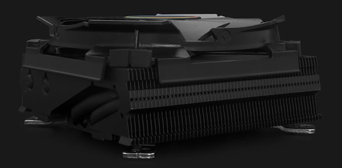
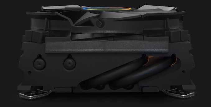
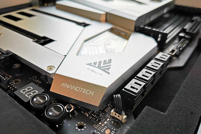
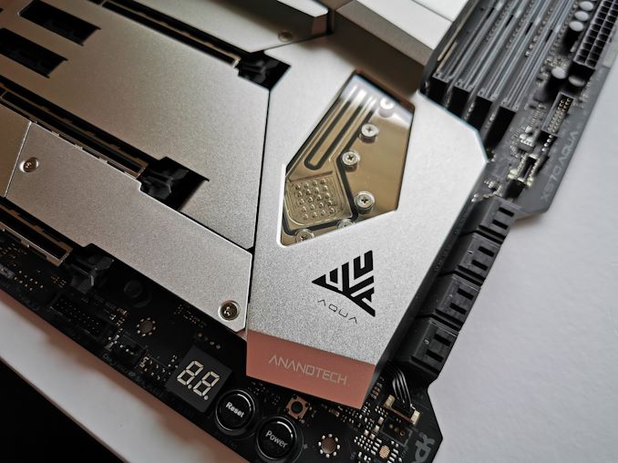
With this, ASRock’s X570 Aqua aims at the upper eschelons of the market, with a full motherboard water block and heatsink combination.


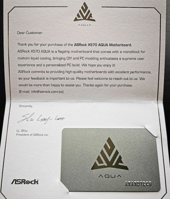
Thank you note and Credit Card style Aqua Card 


Life in Plastic, it’s Fantastic: Nope


Enter the ASRock X570 Aqua with its sleek and robust full cover aluminium armor and a trifecta of water blocks moulded into one unique and custom liquid cooling solution. The aluminium Aqua cooling armor is designed to keep the power delivery, the processor, and the X570 chipset cool, but with added stylings due to integrated addressable RGB LEDs which make the portholes of the blocks look exquisite when in operation. Due to the full cover aluminium armor, it makes this board weigh a considerable amount, but that’s a trade-off from using a quality material over waves of plastic. The two connections to hook up the water block are G1/4 thread which is the most commonly used fitting. We know what’s underneath the chipset section of the block and it’s up to the user as to which processor is used, but underneath the power delivery section is a 14-phase power delivery with 60 A power stages which are designed for enthusiasts.  Providing power to the power delivery is an 8-pin and 4-pin pair of 12 V ATX CPU power inputs. We will be analysing the power delivery in detail in the full review.


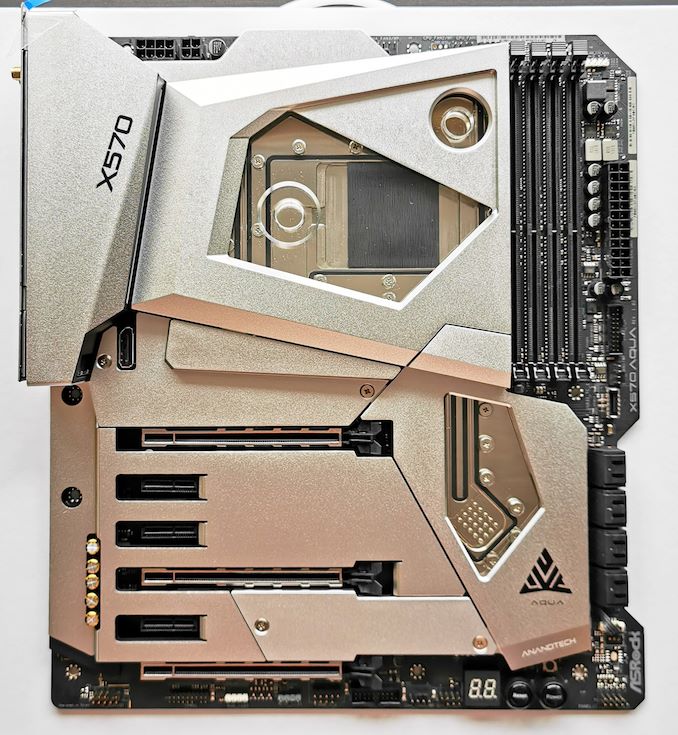
ASRock’s halo X570 Aqua has some very high-end componentry onboard which includes an Aquantia AQC107 10 GbE NIC, with a supplementary Intel I211-AT Gigabit NIC which provides users with dual Ethernet on the rear panel. Also featured is an Intel AX200 Wi-Fi 6 wireless interface which provides both 802.11ax and BT 5.0 connectivity. ASRock has gone all out with its X570 Aqua by validating support for DDR4-5200 memory out of the box across its four available memory slots. This also allows users to install up to and including 128 GB. On the bottom section of the board is three full-length PCIe 4.0 slots which operate at x16, x8/x8, and x8/x8/x4. Sandwiched in between the full-length slots are three PCIe 4.0 x1 slots for users to install additional cards eg, dedicated sound cards, RAID, and networking controllers. At the bottom right-hand side of the PCB is a two-digit LED debugger, a reset switch, and a power switch. Around the board is three 4-pin fan headers split between a CPU fan, a CPU/water pump, and chassis/water pump fan header. This will require users with lots of cooling fans to use splitter cables, a fan hub, or a dedicated fan controller.


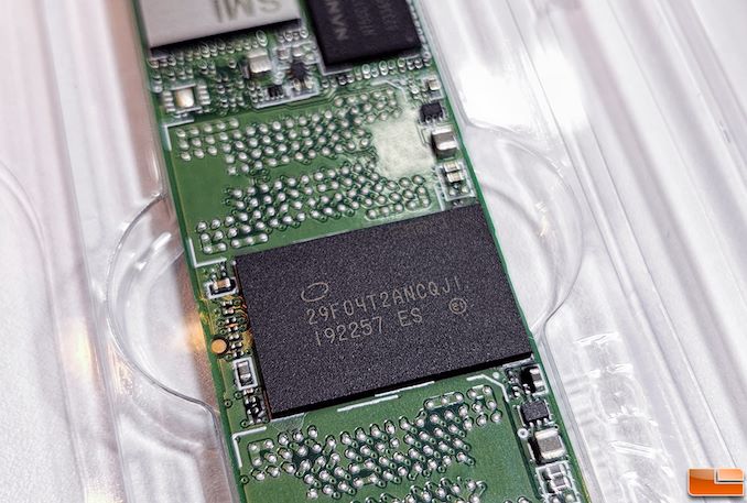
Onto the storage and the X570 Aqua has two PCIe 4.0 x4 M.2 slots which include individual heatsinks, and this model makes use of an ASMedia ASM1061 SATA controller which allows the Aqua to include eight SATA ports; four from the ASM1061 controller and four directly from the X570 chipset. As per the specifications, only the four from the X570 chipset features support for RAID 0, 1, and 10 arrays, but all the SATA ports support AHCI and hot plugging.


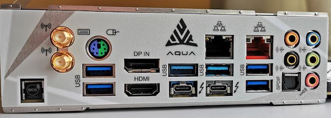
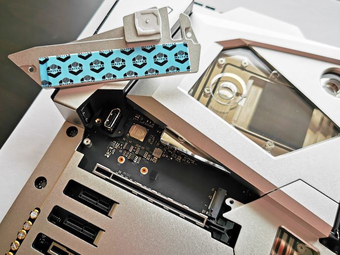
Another prominent feature of the ASRock X570 Aqua is on the rear panel with two Thunderbolt 3 Type-C ports, with a further six USB 3.1 G2 Type-A ports. For users looking to make full use of the graphic output capabilities of the Thunderbolt 3 ports, ASRock has included a single DisplayPort 1.4 input which allows a link between a discrete graphics card and the ports for driving multiple 4K displays from a single video output. A Realtek ALC1220 HD audio codec controllers the five 3.5 mm audio jacks and S/PDIF out on the rear panel, while a Texas Instruments NE5532 is included to improve the front panel audio with capabilities to drive headers of up to 600 Ohms.


It’s not cheap, but why is it $999?


The ASRock X570 Aqua isn’t for everyone and users looking opt for the monolithic E-ATX aluminium clad model will have to use a custom water cooling solution. This will add a further cost on top of the $999 premium ASRock is charging for its X570 Aqua which will see just 999 be made available to the general public. To summarise the breakdown in the cost easily, consider this generations flagship models. X570 flagships this generation seem to cost around $700 (MSI X570 Godlike, GIGABYTE X570 Aorus Extreme, ASUS Crosshair VIII Formula). Factor this into the equation because on paper without the bells and whistles of the aluminium, the ASRock X570 Aqua is flagship level on specifications alone. Doing the math roughly looks a little like this:


  • General Flagship X570 Motherboard – $700
  • EKWB CPU block – $80
  • Current Availablity of X570 chipset blocks – N/A
  • Current Availablity of X570 VRM blocks – N/A

One thing that also has to be factored into the price is exclusivity; there are only 999 units available for purchase. If this works well with the audience, then rarity would add a price premium. By the time you factor in the boards PCB, the full cover aluminium Aqua armor, the cooling provided on the three main areas that require cooling in a system (CPU, power delivery, chipset), it doesn’t make the price seem all that bad. Of course, price is relative to what a user is willing to pay, but the overall package and presentation scream high-end with a mighty roar. With the Ryzen 9 3950X having been pushed back to November, but users looking to overclock it will almost certainly need custom cooling and the Aqua could be the unique route to go down if budget permits it.


Expect the full and detailed review in the coming weeks.


Source: AnandTech – In The Lab: ASRock X570 Aqua Motherboard Preview

AMD Ryzen 9 3900: A 12-Core 65W CPU Listed

A motherboard maker has added support for AMD’s yet-to-be-announced Ryzen 9 3900 CPU. The product will be one of the industry’s first 12-core CPU featuring a mainstream TDP of 65 W. In addition, the same manufacturer revealed that there is a Pro version of the said CPU incoming.


Biostar’s X470NH motherboard recently gained support for AMD’s yet-to-be-announced Ryzen 9 3900 CPU with a 65 W TDP, which may indicate that the launch of the unit is imminent. This is not the first time an unannounced CPU has been listed in a CPU validation list. As a second source, the processor was listed in Eurasian Economic Union’s index of crypto-capable devices as a ‘twelve-core microprocessor’.


AMD Ryzen 3000 9 Series CPUs
AnandTech Cores

Threads
Base

Freq
Boost

Freq
L2

Cache
L3

Cache
PCIe

4.0
TDP Launch Date Price

(SEP)
Ryzen 9 3950X 16C 32T 3.5 4.7 8 MB 64 MB 16+4+4 105W Nov. 2019 $749
Ryzen 9 3900X 12C 24T 3.8 4.6 6 MB 64 MB 16+4+4 105W July 2019 $499
Ryzen 9 3900 12C 24T 3.1 4.2? 6 MB 64 MB 16+4+4 65W ? ?

Based on the information provided by the sources, AMD’s Ryzen 9 3900 is a 12-core CPU with SMT that operates at 3.1 GHz default frequency (and presumably featuring a 4.2 GHz maximum turbo frequency from a 3DMark listing) and a 65 W TDP. The relatively low thermal envelope makes the Ryzen 9 3900 compatible with mainstream motherboards and cooling systems and enables PC makers to build relatively small computers featuring a 12-core processor. Meanwhile, the Ryzen 9 Pro 3900 adds various security technologies, enterprise management, and reliability enhancements for business and corporate computers.


It is unclear when exactly AMD plans to introduce its 12-core Ryzen 9 3900 and Ryzen 9 Pro 3900 processors and how much will they cost, yet it is reasonable to think that both products will be available in the near future.


Related Reading:


Sources: Biostar (via momomo_us/Twitter), EAUnion.org (via Planet3DNow)


Source: AnandTech – AMD Ryzen 9 3900: A 12-Core 65W CPU Listed

Intel Supply in Q4: “Output Capacity up, Supply-Demand Still High”

Recent reports from media outlet Digitimes have stated that Intel’s high demand issue, and its inability to fully supply that demand, will continue into Q4. The report states that Intel’s OEM partners and the supply chain are still short of the supply they are requesting from Intel and its distribution network. We reached out to Intel for comments.


Intel’s high demand has been of particular note since mid-2018. Since the discovery of hardware vulnerabilities such as Spectre and Meltdown, and the fixes that reduced overall performance of a large number of the installed server base, many of Intel customers have been increasing the size of their server deployments in order to re-match their original capacity. This issue caused a sharp up-tick in demand of Intel processors, and Intel has driven newer architectures that try to minimise those performance deficits (with an overall performance uplift when the new architecture is factored in). As a result, Intel moved some of its fabrication capacity away from its future 10nm process and back onto its 14nm in order to meet demand.


The consequence of this is record revenues for Intel – the company shifted a lot of production into its high core count and high-cost parts. The CEO of Intel, Bob Swan, addressed the issue in its recent financial update:


“We’re also making steady progress increasing CPU supply. Through our investments, focused execution and tighter customer collaboration, we expect our PC CPU supply will be up mid single-digits this year while we expect the PC TAM to grow slightly. We’ll continue to work with our customers to meet their required product mix and ramp additional capacity to ensure we are not a constraint on their growth. [] We lost a little bit of share in the second quarter, particularly in CSG at the lower end small core primarily due to supply constraints. So — and our expectation is that we’ll begin to work our way back in the second half of the year given the capacity we’ve put in place to have more supply and meet our customers’ demands.”


The recent report from Digitimes seems to put some cold water on Intel being able to meet all of its 14nm CPU demand by the end of 2019. With the recent launch of Comet Lake in the mobile space, Cascade Lake in the enterprise and workstation space, and the future launches of similar product lines, users and Intel’s partners are expecting a strong supply  of CPUs with the generational update.


We reached out to Intel to see if there was any update to Digitimes’ commentary. An Intel spokesperson stated:


“We continue working to improve the supply-demand balance for our PC customers. In the first half of 2019, we saw PC customer demand that exceeded our expectations and surpassed third-party forecasts. We have added 14nm output capacity and are ramping volume on 10nm with systems on shelf for holiday. While our output capacity is increasing, we remain in a challenging supply-demand environment in our PC-centric business. We are actively working to address this challenge, and we continue to prioritize available output toward the newest generation Intel® Core™ i5, i7 and i9 products that support our customers’ high-growth segments.”


This essentially partially confirms Digitimes’ report. While Intel is increasing its output capacity, with a focus on 10nm as well (Intel reports two fabs on 10nm at this time), the focus on 14nm will be on high-growth segments, which for Q4 is likely to remain the high-end processors. Partners looking at Core i3 and lower performance cores might have to extend their lead-times for CPU supply yet again. It will be interesting to see when Intel will be able to re-reach parity between demand and supply.


Related Reading


Source: AnandTech – Intel Supply in Q4: “Output Capacity up, Supply-Demand Still High”

Intel Announces SSD 665p: Denser, Faster QLC NAND

Intel’s Memory and Storage Day event today in South Korea was mostly focused on enterprise and datacenter products, but they did announce an upcoming consumer SSD: The Intel SSD 665p. This is the successor to the Intel 660p, the first and most successful consumer SSD to use four bit per cell (QLC) NAND flash memory. The 665p isn’t a major update: it keeps the same Silicon Motion SM2263 4-channel controller but updates the NAND to Intel’s second-generation 96-layer 3D QLC NAND. This newer QLC keeps the same 1024Gb per-die capacity while shrinking overall die size, so we don’t expect any change to the range of drive capacities offered nor any major performance changes—but it may lower prices a bit.


Intel showed off the 665p with a live demo pitting the 1TB 660p against a 1TB 665p prototype with pre-production firmware, each installed in otherwise identical ASUS notebooks. Intel used a beta version of CrystalDiskMark 7 to illustrate the 665p’s performance: 40-50% improvement to sequential transfer speeds and about 30% faster random access speeds.


Left: 665p 1TB pre-production Right: 660p 1TB

(Photos by Nathan Kirsch of Legit Reviews)


Caveats: given the short test duration and relatively empty state of the drives, these numbers are measurements only of the SLC cache performance. It’s not clear how much the worst-case write speeds to QLC have changed, and that’s where the 660p falls far behind TLC based SSDs. The sequential IO numbers Intel showed for the 660p are also well below what we’ve measured with the 660p on our own testbed using CDM 7, so the sequential IO improvement might be more along the lines of 20% rather than 40-50%. Our testing of the Intel 660p also showed that it can reach similar speeds of 1.7-1.8GB/s in sequential transfers with a high enough queue depth, so the 665p’s improvement here may amount to extending that performance down to queue depth 1. Either way, it looks like the 665p will be another drive that offers good enough performance for most use cases, but doesn’t really need all four PCIe lanes.


Nathan Kirsch over at Legit Reviews has shared his close-up photos of the 665p alongside the 660p, so we know that the PCB layout is essentially unchanged: a single-sided M.2 2280 drive that only needs to populate all four NAND package locations for the 2TB model.


Intel hasn’t shared the planned launch date for the 665p, but it should be no more than a few months away. Pricing should be comparable to the 660p, making it one of the cheapest consumer NVMe drives on the market.


Source: AnandTech – Intel Announces SSD 665p: Denser, Faster QLC NAND

Intel Shares New Optane And 3D NAND Roadmap – Barlow Pass DIMMs & 144L QLC NAND in 2020

At a press event today in South Korea (?!) Intel shared plans for many of their next round of storage products, including the second generation of Optane enterprise SSDs and Optane DC Persistent Memory modules. They also announced that their next generation of 3D NAND flash memory will use 144 layers and come to market first with QLC-based SSDs, to be followed later by TLC-based SSDs.


It appears that the new Optane products are still using first-generation 3D XPoint memory, though Intel is not confirming that at this time. The Intel-Micron partnership that produced 3D XPoint memory and many generations of NAND flash memory is now ended, but Intel has not announced any plans for high-volume manufacturing of 3D XPoint outside of the IMFT fab in Utah that Micron is keeping in the divorce. Intel is bringing up a “technology development line” for 3D XPoint at a facility in Rio Rancho, NM, but so far this is only being discussed as an R&D location, not a large-scale manufacturing center. Last we heard, the long-term plan was to move 3D XPoint manufacturing to China.


Official electron microscope images of 3D XPoint memory along two axes


Intel’s Optane DC Persistent Memory that attaches directly to the memory controllers of server CPUs using the DIMM form factor was a bit late in coming to market, arriving with the current Cascade Lake-SP generation instead of with Skylake-SP as originally planned. Those first-generation Optane DCPM modules are also known under the codename Apache Pass. Their successor will be the Barlow Pass modules, planned to coincide with Cooper Lake (14nm) and Ice Lake (10nm) server processors scheduled for 2020. Furthermore, Intel’s roadmap extends out for at least two more generations of unnamed DCPM modules to be paired with Sapphire Rapids processors and their successor(s), respectively. Based on previous Intel statements, Sapphire Rapids and third-generation Optane DCPM modules should be using a DDR5 interface. In the more immediate future, the current Apache Pass Optane DCPM modules will soon be arriving in the high-end workstation market alongside Cascade Lake. In the long run, Intel is working with Microsoft to lay the groundwork for persistent memory support in client editions of Windows, but Intel isn’t ready to make specific promises about bringing persistent memory support to their consumer hardware platforms.


Optane “Alder Stream” SSD compared to Optane DC P4800X and SSD DC P4610


On the NVMe SSD side, Intel will be inaugurating the second generation of enterprise Optane SSDs in 2020. The original Optane SSD DC P4800X (codenamed Coldstream) will be replaced by Alder Stream next year. Intel is promising major performance improvements but is being coy about just how big a jump we can expect; they provided a graph that cuts off the end of the curve for Alder Stream but indicates it should at least get close to doubling random IO performance. (Intel’s graph is for 70/30 mixed 4kB random IO.) It wouldn’t be a surprise to see PCIe 4.0 support given the lifespan Intel’s new Optane SSD controller can be expected to have, but the performance data Intel has shared so far doesn’t require more than the current generation’s PCIe 3 x4 interface. After Alder Stream it is reasonable to expect enthusiast derivatives to replace the Optane SSD 900P and 905P, and eventually a replacement for the dual-port Optane SSD DC D4800X, but Intel hasn’t made mention of these yet.


Notably missing from Intel’s presentation is anything new for consumers based on Optane. They are still touting the Optane Memory H10 two-in-one SSD, but the second-generation consumer Optane M.2 drives (Optane Memory M15 and Optane SSD 815P) have been officially cancelled. The 815P is dead because 118GB is simply too small for a standalone SSD to be competitive, and the M15 is dead because there aren’t enough systems still shipping with mechanical hard drives to support another generation of cache drives. The current Optane Memory M10 and Optane SSD 800P are not being discontinued yet.


3D NAND Developments


As for flash-based SSDs, Intel’s presentation focused primarily on QLC NAND. Intel’s SSD 660p is the most successful consumer QLC drive to date, and it will soon be replaced by a 665p that switches to 96-layer QLC from the current 64-layer QLC NAND. This isn’t a full product announcement with specs or an exact release date, but we predict it will not bring major performance changes and will arrive by the end of the year.


Intel’s next generation of 3D NAND after 96 layers will be 144 layers. This will be a QLC-first generation, keeping the same 1Tb die capacity as their 96 and 64-layer QLC. Intel is still committed to their 3D floating gate memory cell design, which they claim provides superior data retention to the charge trap flash designs used by most of their competitors. Intel has not stated whether they are taking their string stacking construction beyond two decks, but it seems most likely that they are reaching 144 layers with something like a 72+72 layer design rather than 48+48+48.


Intel has followed in the footsteps of some of their competitors by bringing up the subject of 5 bit per cell NAND flash to push density beyond QLC (4 bit per cell) NAND flash. Their report is similar to what Toshiba said at Flash Memory Summit: they have it working in the lab, but have not determined if it is feasible for real products.


Intel’s next round of enterprise/datacenter flash-based SSDs will be arriving in 2020, including a 144L QLC SSD. We don’t have any model numbers yet, just codenames. Arbordale+ is tricky to speculate about since the original Arbordale codename was only used internally and didn’t result in any shipping products, so all we know is that it will be a 144L QLC product. Cliffdale-R will be the 96L TLC refresh of the current Cliffdale SSD DC P46xx/45xx family. This probably means that 144L TLC enterprise SSDs won’t be arriving in 2020 and their 144L node will be QLC-only for quite a while. Cliffdale-R should be the first SSDs under Intel’s new naming scheme to occupy the SSD D7 tier.


Related Reading


Source: AnandTech – Intel Shares New Optane And 3D NAND Roadmap – Barlow Pass DIMMs & 144L QLC NAND in 2020

GlobalFoundries Unveils 12LP+ Technology: Massive Performance & Power Improvements

GlobalFoundries has introduced its 12LP+ fabrication process that relies on the groundwork set by its 14LPP and 12LP technologies and provides significant improvements when it comes to performance, power, and area (PPA) scaling. The specialty foundry positions the technology for developers of chips for cloud and edge AI applications.


GlobalFoundries’ 12LP+ manufacturing technology builds upon the company’s 12LP process yet enables a 20% increase in performance (at the same power and complexity) or a 40% reduction in power requirements (at the same clocks and complexity) as well as a 15% improvement in logic area scaling when compared to 12LP platform. Among other things, 12LP+ supports 0.5V SRAM bit cells (which probably use IP that the company designed for its 7 nm nodes). In addition, GF developed a new 2.5D interposer that enables 12LP+ SoCs to work with HBM memory.


Advertised PPA Improvements of New Process Technologies
Data announced by companies during conference calls, press briefings and in press releases
  GlobalFoundries
12LP+

vs 12LPP
12LP

vs 14LPP
14HP

vs 14LPP
GF’s 7nm Gen 1

vs 14LPP
Power 40% ? >60%
Performance 20% 10% ? >40%
Area Reduction 15% 15% ? >50%
 

The foundry says that its 12LP+ uses a mature design and production ecosystem and provides advantages comparable to those of 7 nm-class fabrication process. Meanwhile, significant improvements and a new PDK point to new design libraries along with numerous new features, which means that GlobalFoundries’ clients will have to make significant investments in order to take advantage of 12LP+. Those investments will still be 50% lower than the cost of transition to a 7 nm-class technology, according to GlobalFoundries.


Michael Mendicino, vice president of Digital Technology Solutions at GF, said the following:


“Our 12LP+ solution already offers clients a majority of the performance and power advantages they would expect to gain from a 7nm process, but their NRE (non-recurring engineering) costs will average only about half as much, a significant savings. Additionally, because the 12 nm node has been running longer and is much more mature, clients will be able to tape-out quickly and take advantage of the growing demand for AI technology.”


To speed up development of 12LP+ chips for its clients, GlobalFoundries has asked Arm to design Arm Artisan physical IP and POP IP required by AI-focused SoCs. That IP is said to be compatible with 12LP. Meanwhile, the 12LP+ PDK is already available and several clients have begun to design chips using the technology. GlobalFoundries expects its customers to tape out the first 12LP+ SoCs sometimes in the second half of 2020 and produce them in volume in 2021.


GlobalFoundries will manufacture 12LP+ chips using deep ultraviolet (DUV) lithography with argon fluoride (ArF) excimer lasers operating on a 193 nm wavelength at its Fab 8 in New York, USA. Presumably, the company will use the same equipment that is currently used to make SoCs at 12LP and 14LPP nodes.


Related Reading:


Source: GlobalFoundries


Source: AnandTech – GlobalFoundries Unveils 12LP+ Technology: Massive Performance & Power Improvements

The Black Shark 2 Review: A Gaming Phone's Existential Crisis

Over the last 1-2 years we’ve seen a new type of smartphone category start carving itself a niche in the market: the gaming smartphone. Last year, the original Black Shark was amongst the first devices to try to cater to a gaming audience, offering characteristic “gaming designs” as well as promising to offer software features to differentiate itself from the more usual smartphone offerings.


This year, Xiaomi has updated its Black Shark line and brand with the new Black Shark 2. The phone is very much a continuation of what we saw last year with the Black Shark, but offering the newest hardware innards and iterative improvements to the design and features.


Source: AnandTech – The Black Shark 2 Review: A Gaming Phone’s Existential Crisis