Qualcomm Unveils Snapdragon 4 Gen 2: Modest Modernization For Low-End Mobiles

Qualcomm this morning is taking the wraps off its next generation Snapdragon 4-class mobile SoC, the aptly named Snapdragon 4 Gen 2. The company’s new entry-level SoC for smartphones and other devices incorporates some hardware updates that should modestly boost performance for the most cost-sensitive segment of the mobile market, as well as bringing Qualcomm’s overall Snapdragon product stack into closer alignment by supporting more recent 5G standards and fabbing the chip to a newer process node.


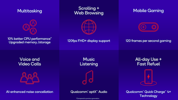
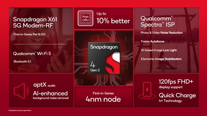
First and foremost, the top line on performance is that Qualcomm is touting a 10% boost in CPU performance, thanks to higher CPU core clockspeeds. The Snapdragon 4 Gen 2 uses the same 2+6 CPU core configuration as its predecessor, the Snapdragon 4 Gen 1, with 2 Cortex-A78-derived Kryo CPU cores paired with 6 Cortex-A55-derived cores. Thanks to a node shrink, Qualcomm has boosted the top clockspeeds on each set of cores by about 10%, bringing the A78 cores up to 2.2GHz, and the A55 cores up to 2.0GHz. So the 10% CPU performance gain should be fairly consistent in both single and multi-threaded workloads.


Architecturally, there’s little to say about these cores that hasn’t been said already. These are reasonably performant CPU cores, though the age and the lack of higher clockspeeds means their performance potential is limited. The ultra-budget nature of the Snapdragon 4 series means this will be the last part of Qualcomm’s stack to move to any kind of Armv9 core. Though interestingly, the 4 Gen 2 does get a bit of a leg up over the 6 Gen 1 when it comes to the A55 cores – 6G1’s small cores only boost to 1.8GHz, despite being fabbed on the same process node. So this will narrow the CPU performance gap between those parts a bit (at least until the obligatory 6 Gen 2 lands).


Meanwhile, Qualcomm is staying mum on GPU performance. The company stopped giving their GPUs external product numbers a few years ago, and for the Snapdragon 4 release they are not even issuing performance expectations. So we aren’t expecting any gains here, especially as the chip is still meant to drive HD/FHD devices.


Qualcomm Snapdragon 4-Series SoCs
SoC Snapdragon 4 Gen 2

(SM4450)
Snapdragon 4 Gen 1

(SM4375)
Snapdragon 480

(SM4350)
CPU 2x CA78

@ 2.2GHz 


6x CA55

@ 2.0GHz
2x CA78

@ 2.0GHz 


6x CA55

@ 1.8GHz
2x CA76

@ 2.0GHz


6x CA55

@ 1.8GHz
GPU Adreno Adreno Adreno 619
DSP Hexagon Hexagon Hexagon 686
ISP/

Camera
Spectra

(2x 12-bit)


1x 10⁸MP or 32MP with ZSL

or

16+16MP with ZSL


Spectra

(3x 12-bit)


1x 10⁸MP or 32MP with ZSL

or

25+13MP with ZSL

or

3x 13MP with ZSL

 
Spectra 345

(3x 12-bit)


1x 64MP

or

25+13MP

or

3x 13MP
Encode/

Decode
1080p60

H.264, H.265, VP9 (Decode-Only)
Memory 2x 16-bit @ 3200MHz

LPDDR5X

25.6GB/s

or

2x 16-bit @ 2133MHz

LPDDR4X

17.0GB/s
2x 16-bit @ 2133MHz

LPDDR4X

17.0GB/s
2x 16-bit @ 2133MHz

LPDDR4X

17.0GB/s
Storage UFS 3.1 (2 lane) UFS 2.2, eMMC 5.1 UFS 2.2, eMMC 5.1
Integrated Modem X61 Integrated


LTE

DL = 800Mbps

UL = 210Mbps


5G NR

Sub-6

(100MHz)


DL = 2500Mbps

UL = 900Mbps
X51 Integrated


LTE

DL = 800Mbps

UL = 210Mbps


5G NR

Sub-6 + mmWave

(100MHz)


DL = 2500Mbps

UL = 900Mbps
X51 Integrated


LTE

DL = 800Mbps

UL = 210Mbps


5G NR

Sub-6 + mmWave

(100 + 200MHz)


DL = 2500Mbps

UL = 660Mbps
Wi-Fi/BT Wi-Fi 5 (2×2)

Bluetooth 5.1
Wi-Fi 5 (2×2)

Bluetooth 5.2
Wi-Fi 5 (2×2)

Bluetooth 5.1
Mfc. Process Samsung 4nm TSMC 6nm Samsung 8nm LPP


As noted earlier, Qualcomm has moved their entry-level SoC to a Samsung 4nm process (given the timing, 4LPP, we’d assume). That means that Samsung’s entire current product stack – Snapdragons 8G2, 7+G2, 6G1, and 4G2 – are all made on a 4nm node of some flavor. Samsung’s is the less performant of the two, but it’s almost certainly cheaper. Which is a boon for these entry-level, price-constrained parts. Academically, I’m curious just how small the Snapdragon 4 die is based on this process, as it should be rather tiny, but that’s not a detail Qualcomm normally shares.


Otherwise, this latest Snapdragon 4-class SoC is a bit of a give-and-take release as compared to the 4 Gen 1. On the memory side of matters, the new SoC incorporates Qualcomm’s newer controller design, bringing LPDDR5X support to a 4-class chip for the first time. Like other Qualcomm SoCs, the chip can run that memory at up to LPDDR5X-6400 speeds. Meanwhile, LPDDR4X remains supported as well, at the usual LPDDR4X-4266 data rate. The memory bus is still a total of 32-bits wide, so you’re looking at a peak memory bandwidth of 25.6GB/second with LPDDR5X, a full 50% more bandwidth than what the 4 Gen 1 could provide.


The storage controller has also been updated to support UFS 3.1, finally bringing Qualcomm’s low-end chip up to relatively modern version of the flash storage standard. Compared to the UFS 2.2 spec supported in the previous chip, UFS 3.1 a bit more than doubles the bandwidth per lane; so in a two-lane configuration, the 4G2 can theoretically transfer as much as 2.9GB/second of data though Qualcomm isn’t making any performance claims. Notably, eMMC storage support is absent from Qualcomm’s specification sheet, indicating that support for that now well-outdated interface standard is finally riding off into the sunset.


As for Qualcomm’s imaging ISPs and related hardware, the 4 Gen 2 will be taking a step backwards by removing the third camera pipeline. As a result, 4 Gen 2 will only support up to two cameras. The Spectra ISPs themselves are seemingly unchanged, with Qualcomm still using their 12-bit designs. Due to that camera shift, the overall imaging capabilities of the SoC have changed a bit, even in a two camera configuration. The resolutions supported in dual camera zero shutter lag mode are now balanced; rather than 25+13MPixels, the SoC runs at (up to) 16+16Mpixels.


Though with fewer camera modules to support, Qualcomm is touting better camera performance. In particular, Qualcomm says that the new SoC offers faster autofocus support than the 4 Gen 1, as well as an updated electronic image stabilization feature. The 4 Gen 2 also includes an “AI-enhanced” low light feature, and multi-camera temporal filtering (MCTF) support has been baked into the SoC for noise reduction.


The other major hardware improvement for the SoC, in turn, is an upgrade to a Snapdragon X60-series class modem. New to Qualcomm’s product lineup is the Snapdragon X61 modem, a downscaled version of their X62/X65 modem seem in other chips. Relative to the outgoing 4 Gen 1 SoC and its X51 modem, the X61 supports the newer Release 16 version (aka 5G Phase 2) of the 3GPP standard family.


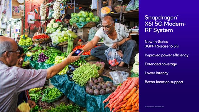
Release 16 is now coming up on 3 years old, so this is a needed update to keep up with 5G network development. Though because the primary benefits of Release 16 are more for the network operations side than the consumer side, phone buyers don’t often see much from it besides some improvements in coverage. In the case of the 4 Gen 2, the actual bandwidth figures are unchanged from the 4 Gen 1, which means downloads and uploads top out at 2.5Gbps and 900Mbps respectively.


mmWave support has also remained off of Qualcomm’s spec sheets this time around. On the 4 Gen 1 it ended up being an unlisted feature of sorts – the hardware was there in case any handset vendor wanted to use it, but Qualcomm didn’t advertise it – and it’s unclear whether Qualcomm even bothered with the hardware for this new silicon.


Also of note: Bluetooth 5.2 support has disappeared from Qualcomm’s specifications. Whereas the 4 Gen 1 supported BT 5.2, across Qualcomm’s documentation 4 Gen 2 is listed as only supporting BT 5.1. This is notable not only because it’s a regression, but because Bluetooth Low Energy Audio is a 5.2 feature – and arguably the defining feature of 5.2. At this point it’s unclear why Qualcomm would want to remove the feature from their low-end SoC (I suspected royalties, but the LC3 codec for LE Audio is part of the BT license). Otherwise, the Wi-Fi half of Qualcomm’s radio system remains unchanged, with Wi-Fi 5 support.


Wrapping things up, Qualcomm tells us that several of the usual suspects will be adopting the Snapdragon 4 Gen 2, including Redmi and vivo. Handsets based on the SoC are expected to be announced in the second half of this year.


Source: AnandTech – Qualcomm Unveils Snapdragon 4 Gen 2: Modest Modernization For Low-End Mobiles

Gigabyte's Low-Cost Mini-ITX A620 Motherboard Supports Ryzen R9 7950X, R9 7950X3D CPUs

Gigabyte has quietly introduced one of the industry’s first inexpensive motherboards for AMD’s AM5 processors in Mini-ITX form-factor. The most unexpected peculiarity of Gigabyte’s A620I AX motherboard — based on AMD’s low-cost A620 chipset that only supports essential features — is that it supports AMD’s top-of-the-range Ryzen 9 7950X3D and Ryzen 9 7950X processors.


Despite its positioning as an entry-level motherboard for AMD’s Ryzen 7000-series CPUs based on the Zen 4 microarchitecture, Gigabyte’s Ultra Durable A620I-AX can handle all of AMD’s AM5 CPUs released to date, including relatively inexpensive Ryzen 5 7600 with a 65W TDP as well as range-topping Ryzen 9 7950X3D with 3D V-Cache rated for 120W and Ryzen 9 7950X rated for 170W. Given that AMD’s A620 platform is not meant for overclocking, the Ryzen 9 7950X cannot be overclocked on this motherboard, but even support of this CPU is unexpected. 


AMD’s Ryzen 7000-series CPUs are hungry for memory bandwidth and the UD A620I-AX does not disappoint here as it comes with two slots for DDR5 memory that officially support memory modules rated for up to DDR5-6400 and with EXPO profiles. High-performance DDR5 DIMMs will be beneficial not only for Ryzen 9 and Ryzen 7 CPUs aimed at demanding gamers, but will also be beneficial for cheap PCs running AMD’s upcoming AM5 APUs with built-in graphics as memory bandwidth is crucial for integrated GPUs. The motherboard even has two display outputs to support iGPUs.


Speaking of gaming, the UD A620I-AX motherboard naturally lacks any kind of PCIe Gen5 support, but it does have a PCIe 4.0 x16 slot for graphics cards and an M.2-2280 slot with a PCIe 4.0 x4 interface for SSDs. For those who need additional storage space, the platform has two SATA ports.


As for overall connectivity, the UD A620I-AX motherboard features a Wi-Fi 6 + Bluetooth adapter, an 2.5GbE port, USB 3.2 Gen1/2 ports (including a Type-C port), and audio connectors. While this may not seem much, entry level gaming systems do not use a lot of high-performance peripherals anyway. Furthermore, AMD’s A620 platform does not support USB4.


Pricing details for the UD A620I-AX are not yet available, but some early reports suggest that it will be priced below/around $100, like other A620-based offerings. Meanwhile, given support for high-end Ryzen 9 processors and Mini-ITX form-factor, it is possible that Gigabyte may charge a premium for the UD A620I-AX. Therefore, it remains to be seen how reasonably priced will this motherboard be when it hits the market.


Source: AnandTech – Gigabyte’s Low-Cost Mini-ITX A620 Motherboard Supports Ryzen R9 7950X, R9 7950X3D CPUs

The Aurora Supercomputer Is Installed: 2 ExaFLOPS, Tens of Thousands of CPUs and GPUs

Argonne National Laboratory and Intel said on Thursday that they had installed all 10,624 blades for the Aurora supercomputer, a machine announced back in 2015 with a particularly bumpy history. The system promises to deliver a peak theoretical compute performance over 2 FP64 ExaFLOPS using its array of tens of thousands of Xeon Max ‘Sapphire Rapids’ CPUs with on-package HBM2E memory as well as Data Center GPU Max ‘Ponte Vecchio’ compute GPUs. The system will come online later this year.


“Aurora is the first deployment of Intel’s Max Series GPU, the biggest Xeon Max CPU-based system, and the largest GPU cluster in the world,” said Jeff McVeigh, Intel corporate vice president and general manager of the Super Compute Group.


The Aurora supercomputer looks quite impressive, even by the numbers. The machine is powered by 21,248 general-purpose processors with over 1.1 million cores for workloads that require traditional CPU horsepower and 63,744 compute GPUs that will serve AI and HPC workloads. On the memory side of matters, Aurora has 1.36 PB of on-package HBM2E memory and 19.9 PB of DDR5 memory that is used by the CPUs as well as 8.16 PB of HBM2E carried by the Ponte Vecchi compute GPUs. 


The Aurora machine uses 166 racks that house 66 blades each. It spans eight rows and occupies a space equivalent to two basketball courts. Meanwhile, that does not count the storage subsystem of Aurora, which employs 1,024 all-flash storage nodes offering 220TB of storage capacity and a total bandwidth of 31 TB/s. For now, Argonne National Laboratory does not publish official power consumption numbers for Aurora or its storage subsystem.


The supercomputer, which will be used for a wide variety of workloads from nuclear fusion simulations to whether prediction and from aerodynamics to medical research, uses HPE’s Shasta supercomputer architecture with Slingshot interconnects. Meanwhile, before the system passes ANL’s acceptance tests, it will be used for large-scale scientific generative AI models.


While we work toward acceptance testing, we are going to be using Aurora to train some large-scale open-source generative AI models for science,” said Rick Stevens, Argonne National Laboratory associate laboratory director. “Aurora, with over 60,000 Intel Max GPUs, a very fast I/O system, and an all-solid-state mass storage system, is the perfect environment to train these models.


Even though Aurora blades have been installed, the supercomputer still has to undergo and pass a series of acceptance tests, a common procedure for supercomputers. Once it successfully clears these and comes online later in the year, it is projected to attain a theoretical performance exceeding 2 ExaFLOPS (two billion billion floating point operations per second). With vast performance, it is expected to secure the top position in the Top500 list.


The installation of the Aurora supercomputer marks several milestones: it is the industry’s first supercomputer with performance higher than 2 ExaFLOPS and the first Intel’-based ExaFLOPS-class machine. Finally, it marks the conclusion of the Aurora saga that began eight years ago as the supercomputer’s journey has seen its fair share of bumps.


Originally unveiled in 2015, Aurora was initially intended to be powered by Intel’s Xeon Phi co-processors and was projected to deliver approximately 180 PetaFLOPS in 2018. However, Intel decided to abandon the Xeon Phi in favor of compute GPUs, resulting in the need to renegotiate the agreement with Argonne National Laboratory to provide an ExaFLOPS system by 2021.


The delivery of the system was further delayed due to complications with compute tile of Ponte Vecchio due to the delay of Intel’s 7 nm (now known as Intel 4) production node and the necessity to redesign the tile for TSMC’s N5 (5 nm-class) process technology. Intel finally introduced its Data Center GPU Max products late last year and has now shipped over 60,000 of these compute GPUs to ANL.


Source: AnandTech – The Aurora Supercomputer Is Installed: 2 ExaFLOPS, Tens of Thousands of CPUs and GPUs

Intel Discontinues Arc A770 Limited Edition Graphics Card

In a rather unexpected move, Intel this week discontinued its Arc A770 Limited Edition graphics card, which was its flagship discrete graphics offering for desktops. Intel’s partners will continue to offer their Arc A770 add-in-boards (AIBs) with 8 GB and 16 GB of GDDR6 memory.


Intel discontinues its Arc A770 Limited Edition graphics card rather abruptly: the company listed June 20, 2023 as the last product order date and the last product shipment date, which essentially means that it no longer produces and ships these boards. As soon as the remaining stock of these products will be depleted in the channel, they will no longer be available. Apparently, the product was a Limited Edition indeed since it is being EOLed less than a year on the market.


A quick check at Amazon and Newegg reveals that the Arc A770 LE board is available for as much as $497.35 at Amazon and is no longer available at Newegg. Meanwhile, Newegg has three CPU + A770 graphics cards bundles containing Acer’s Predator BiFrost Arc A770 16 GB AIBs. Separately, this board costs $339 at Newegg.


Intel’s own Arc A750 Limited Edition and Arc A770 Limited Edition graphics cards were meant to bring the audience the best experience possible with an all-new GPU family. In addition, they demonstrated that Intel wanted its Arc A700-series products to compete for the mainstream market segment without using fancy and huge cooling systems. Indeed, Intel’s own Arc A750 LE and Arc A770 LE boards look very modest, yet provided everything that the company’s ACM-G10 GPU had to offer in terms of performance and functionality.


By now, there are Intel Arc A770 graphics cards from numerous AIB producers, including ASRockAcerGigabyteGunnirMSI, and Sparkle, so Intel does not really need to offer its own cards to ensure that its top-of-the-line product is present on the market.


Interestingly, but Intel’s Arc A750 Limited Edition graphics cards remains afloat for now. Perhaps, while Intel still has these boards in its own stock.


Source: Intel


Source: AnandTech – Intel Discontinues Arc A770 Limited Edition Graphics Card

Transcend ESD310C Dual-Interface UFD Review: Silicon Motion Powers Portable SSD in a Thumb Drive

Transcend recently introduced the ESD310C portable SSD in a thumb drive form-factor. A compact device with both Type-A and Type-C USB 3.2 Gen 2 (10 Gbps) interfaces, the ESD310C is also attractively priced. The product is based on Silicon Motion’s SM2320 native USB flash drive controller, and is quite similar to the Kingston DataTraveler Max A in terms of internal components. Read on to find out what the SM2320 can deliver in a slightly different form factor, and how Transcend manages to differentiate the ESD310C from the other 10 Gbps thumb drives in the market.


Source: AnandTech – Transcend ESD310C Dual-Interface UFD Review: Silicon Motion Powers Portable SSD in a Thumb Drive

Intel Sells a 20% Stake in Maker of Multi E-Beam Mask Writing Tools

Intel on Wednesday announced that it had agreed to sell a 20% stake in IMS Nanofabrication, a company the develops and builds multi e-beam photomask writing tools, for $860 million. The move provides Intel much needed cash and allows IMS to engage into deeper cross-industry collaboration.


IMS Nanofabrication develops and builds multi e-beam tools that synthesize photomasks (reticles). Using multiple e-beams to print a photomask greatly speeds up the process, which is important as photomasks tend to wear out when extreme ultraviolet (EUV) lithography is used. In addition, using multi e-beam tools allows Intel to quickly introduce small changes to pellicles to enhance performance and/or yields. Finally, using multi e-beam tools could be crucial for production of photomasks for next generation nodes that rely on EUV and eventually on High-NA EUV lithography.


Intel first invested in IMS back in 2009 and then acquired the company in 2015. Following the takeover, IMS quadrupled its employee base and manufacturing capabilities and also released three generations of e-beam mask writing products.


This week Intel agree to sell roughly 20% of IMS Nanofabrication to Bain Capital in a deal that values IMS at roughly $4.3 billion. The transaction is expected to close in Q3 and after that IMS will function independently with Dr. Elmar Platzgummer continuing in his role as CEO.


“The advancement of lithography is critical to driving continued progress in the semiconductor industry, and mask writing plays a central role in the industry’s transition to new patterning technologies, such as high-NA EUV,” said Matt Poirier, senior vice president of Corporate Development at Intel. “Bain Capital’s investment and partnership will provide IMS with increased independence and bring strategic perspective to help accelerate the next phase of lithography technology innovation, ultimately benefitting the ecosystem as a whole.”


Selling a 20% stake in fab tool company provides Intel some $860 million, which is not bad for a company that has been bleeding money for some time now. Meanwhile, selling ownership in fab tool makers fits into Intel’s general strategy. For example, back in the day the company bought stock of ASML in a bid to help the company finance development of EUV wafer fab equipment and then sold it stake in ASML. 


While controlling an important EUV vendor could give a competitive edge, it slowdowns creation of industry standards that are crucial for high-volume chip production. 


Thriving semiconductor production industry is more important than making short-term profits, which is why Intel is not afraid of selling off its shares of companies like ASML or IMS and provide some benefits to its rivals.


“[Bain Capital] sharse our conviction in the meaningful opportunity ahead for IMS as EUV becomes more pervasive and high-NA EUV moves from development into high-volume manufacturing in the second half of the decade,”Platzgummer said. “We look forward to expanding our ability to support the world’s largest chip producers, who rely on our technology to produce current and next generations of semiconductor products.”


Source: Intel


Source: AnandTech – Intel Sells a 20% Stake in Maker of Multi E-Beam Mask Writing Tools

Micron Unveils First UFS 4.0 Modules: Up to 4,300 MB/s Storage for Smartphones

Micron on Wednesday introduced its first UFS 4.0-compliant storage devices. The company’s latest generation of single-module smartphone storage devices are slated to be the fastest yet, offering a combination of improvements coming from the UFS specification itself, along with including newer, faster NAND within the storage devices. Micron expects its UFS 4 devices to be used by upcoming flagship smartphones, tablets, and ultra-low-power notebooks already this year.


Micron’s UFS 4.0 storage devices come in three capacities — 256 GB, 512 GB, and 1 TB — that rely on the company’s own controller. The higher-end 512 GB and 1 TB UFS 4.0 products use Micron’s 232-layer six-plane 1 Tb 3D TLC NAND devices and can provide sequential read speed of up to 4,300 MB/s as well as sequential write speed of up to 4,000 MB/s, which makes them the highest performing UFS storage modules for smartphones to date, based on data supplied by Micron. The 256 GB unit is slightly slower as it uses quad-plane 3D NAND devices.


The new UFS 4.0 storage modules from Micron are fully compliant with the specification and use two M-PHY Gear 5 lanes for data transmission. In addition, they support such proprietary firmware capabilities as Data Stream Separation (separates frequently used and rarely data on the device to reduce background garbage collection), Auto Read Burst (improves read performance by using device de-fragmentation after it is used for a long time), and Eye Monitoring (ensures signal integrity).


In addition to offering higher performance than predecessors, Micron’s UFS 4.0 modules are said to feature a 25% higher energy efficiency achieved through a combination of higher performance and energy saving capabilities.


“Micron’s latest mobile solution tightly weaves together our best-in-class UFS 4.0 technology, proprietary low-power controller, 232-layer NAND and highly configurable firmware architecture to deliver unmatched performance,” said Mark Montierth, corporate vice president and general manager of Micron’s Mobile Business Unit.


Usage of high-capacity 232-layer 3D TLC NAND devices also enables Micron to make its UFS 4.0 modules rather thin. The company says that their z-height does not exceed 0.8 – 0.9 mm, which will enable makers of handsets to either make their products slimmer, or fit in a higher-capacity battery.


Micron is currently sampling its UFS 4.0 storage modules with leading smartphone makers and expects these units to be used in the coming months or quarters after it starts mass production in the second half of the year.


Source: AnandTech – Micron Unveils First UFS 4.0 Modules: Up to 4,300 MB/s Storage for Smartphones

Intel to Spend Tens of Billions on New Fabs in Germany and Israel

Intel is spending tens of billions of dollars on new fabs in Arizona and Oregon, but the company’s ambitions certainly do not end in the U.S. This month the company revealed its finalized plans for new production capacities in Europe and Middle East with intentions to invest over $50 billion. 


Intel’s new ‘Silicon Junction’ site near Magdeburg, Germany, will accommodate at two fabs and will initially cost €30 billion. The manufacturing facilities will make chips on an ‘Angstrom-era’ node, though Intel does not disclose which one for now. The only thing that the company reveals for now is that the production node will be more advanced than the one Intel envisioned for the fab originally, which can point to nodes that are more advanced than Intel 20A and Intel 18A. The property needed for this upcoming project was purchased by Intel in November 2022. After the European Union greenlights the incentive package, the first fab will be up and running within four to five years, Intel claims.


Intel disclosed original plans for a chip plant near Magdeburg, Germany, in early 2022. Back then, the fab was estimated to cost $18.7 billion, and the German government agreed to provide $7.2 billion in state aid. However, Intel later chose to broaden the project’s scope, intending to construct a bigger and more technologically advanced plant with total investments amounting to $31.675 billion (€30 billion). This expansion necessitated additional subsidies, leading to prolonged negotiations between Intel and the German authorities. Finally, a revised agreement was reached this week, granting Intel €10 billion ($10.91 billion) in government aid for the construction of the new fab.


Alongside developing a brand new fab complex in Germany, Intel has plans to extend its site in Kiryat Gat, Israel. The CPU giant is slated to invest some $25 billion into constructing and equipping this new Israeli fab, as reported by Benjamin Netanyahu, Israel’s prime minister. This signifies the most substantial foreign investment ever received by Israel.


The new Kiryat Gat facility is set to start production in 2027 and is expected to operate until at least 2035, which, according to the Israeli Finance Ministry, should create thousands of well-paid jobs. Under the terms of this deal, Intel will see its tax rate increase from the present 5% to 7.5%.


Building new fabs in will significantly increase Intel’s manufacturing capacities available for its own products and for chips designed by clients of its Intel Foundry Services unit. In addition to advanced chip production facilities in Germany and Ireland, the company will also construct a new advanced packaging facility near Wroclaw, Poland, which will allow Intel to build and package chips entirely in Europe instead of bringing them to Asia for packaging.


This new advanced packaging facility near Wroclaw, Poland, is projected to fulfill the critical need for assembly and testing capacity that Intel foresees by 2027. The company plans to invest up to $4.6 billion into the project, designed to allow for future expansion. Upon completion, it is expected to employ about 2,000 staff members.


Sources: IntelIntelReuters


Source: AnandTech – Intel to Spend Tens of Billions on New Fabs in Germany and Israel

Noctua's New Cooler Mounting to Lower Temps of AMD's AM5 CPUs

AMD’s latest Ryzen 7000-series CPUs in AM5 packaging are well known for their high operating temperatures. Higher-performance coolers like all-in-one liquid cooling systems have typically solved the problem. Noctua seems to have a different method of improving cooling performance without spending much on a cooler. Apparently, offsetting the CPU cooler mount by 7 mm can reduce the processor’s temperature by up to 3°C.


There are several reasons why AMD’s Ryzen 7000-series processors based on the Zen 4 microarchitecture require better cooling than their predecessors. First, they have a thicker integrated heat spreader (IHS) than their ancestors, perhaps to maintain compatibility with AM4 coolers. Secondly, the position of Ryzen 7000’s core complex dies (CCDs) closer to the southern edge of the socket further complicates cooling. Noctua has discovered that optimizing the position of the heatsink over these CCDs and enhancing the contact pressure dramatically improves the cooler’s performance and reduces CPU temperatures.


Variables like heat flux densities, CPU and radiator tolerances, and thermal paste application can cause results to vary. Still, according to Noctua, the new mounting offset can often decrease core temperatures by 1–3°C for top-tier AM5 CPUs. These reductions can lead to a more efficiently cooled CPU, higher boost clocks, or reduced fan speeds and noise levels. These benefits are especially important for gaming systems that use the latest and greatest processors and graphics cards. Meanwhile, the new bars can also improve the cooling of AM4 CPUs.


“We have experimented with offset mountings ever since AMD introduced its first chiplet processors that had the hotspot shifted towards the south side of the socket, but on AM4, we only saw relatively small improvements in the range of 0.5-1°C”, said Roland Mossig, Noctua CEO. “With the new AM5 platform and its different heat-spreader design, we achieved typical improvements in the range of 1-3°C, so we think this will be a very interesting performance upgrade for Ryzen 7000 users!”


Noctua plans to update bundles of its coolers to include the offset bars, but this will not happen until Q4 2023. To that end, Noctua will offer its customers to obtain one of the four mounting kits — the NM-AMB12, NM-AMB13, NM-AMB14, and NM-AMB15 — for their existing AM4 and AM5 coolers either directly or from Amazon for a symbolic price.


Source: Noctua


Source: AnandTech – Noctua’s New Cooler Mounting to Lower Temps of AMD’s AM5 CPUs

The Razer Blade 14 (2023) Laptop Review: Ryzen 9 7940HS Tested With GeForce RTX 4070 Graphics

Perhaps one of the most popular brands in the realm of gaming, if not the most popular, is Razer. Offering products across multiple categories, although primarily renowned for their peripherals, they officially threw their hat into the notebook arena in 2012 with the Razer Blade. Over the last eleven years, the Razer Blade has constantly evolved with many different variants available, with different screen sizes and form factors such as the Blade 13, 14, 15, 16, and 17; Razer also has the Blade Stealth and the Blade Pro series.


The latest Razer Blade 14 (2023) comes equipped with AMD’s latest Ryzen 7040HS series processor, the Ryzen 9 7940HS, which has eight highly efficient yet potent Zen 4 cores and comes with one of two mobile graphics cards; NVIDIA’s mobile-focused RTX 4060 or the RTX 4070 which drives the 14″ 2560 x 1600p (16:10) IPS display. Available at launch in three configurations, today we’ll be taking a look at the middle of the three Razer Blade 14’s with 16 GB of DDR5-5600 memory, Ryzen 9 7940HS 8C/16T processor, and NVIDIA’s RTX 4070 with 8 GB of GDDR6 VRAM.


Source: AnandTech – The Razer Blade 14 (2023) Laptop Review: Ryzen 9 7940HS Tested With GeForce RTX 4070 Graphics

Broadcom Updates Wi-Fi 7 Portfolio with Lower Cost Second Generation Silicon

Wi-Fi 7 has been gaining slow traction in the market over the last few quarters. Despite a large number of product announcements towards the end of last year (including the usual suspects – ASUS, Netgear, and TP-LINK), only TP-LINK seems to have started actual shipment to end users. On the silicon side, Mediatek was the first to announce both access point and client platforms under the Filogic 880 / Filogic 380 solutions in early 2022. Broadcom followed suit with the BCM67263 / BCM6726 for residential APs, BCM43740 / BCM43720 for enterprise APs, and the BCM4398 for client devices. Qualcomm was not to be left behind, and launched their Wi-Fi 7 Networking Pro series in May 2022 (after introducing the client-focused FastConnect 7800 in February 2022). Over the last year, Qualcomm has been marketing their FastConnect 7800 and Networking Pro Series Wi-Fi 7 platform as the only solution in the market to support the high-band simultaneous multi-link operation mode.


Today, Broadcom is announcing their second-generation Wi-Fi 7 platform, with the aim of addressing cost-effectiveness and achieving competitive parity.


The first-generation products in the AP category in the above comparison were both quad-stream. In order to optimize cost and get deployed in a wider range of products, the two new AP platforms have a dual 2×2 configuration and can operate in all three bands simultaneously. PHY rate drops from 11.5 Gbps to 8.64 Gbps because of the reduction in stream count.


Broadcom 2nd Gen. 802.11be (Wi-Fi 7) Access Point Radios Specifications
  BCM6765 BCM47722
Target Market Residential Wi-Fi APs Enterprise Wi-Fi APs
Operational Bands 2.4 GHz, 5 GHz, and 6 GHz
Stream Count Dual 2×2
Max. Channel Width 320 MHz
PHY Rate 8.64 Gbps
Additional Radios / Protocol Support   BLE, Zigbee, and Thread


The enterprise Wi-Fi AP platform (BCM47722) now integrates Bluetooth and Zigbee / 802.15.4 support in order to cater to IoT requirements. Both AP platforms come with an integrated quad-core ARMv8 CPU and 10G PHY, which pulls in some of the features from the BCM4916 network processor used in the first-generation platforms. Some of the other key features include the ability of the platforms to support simultaneous operation in any of the three bands, integrated 2.4 GHz power amplifiers and miscellaneous updates to reduce power consumption. The new platforms enable tri-band MLO, which provides significant latency benefits, particularly in highly congested networks.


On the client side, the BCM4390 is being offered as a cost-effective Wi-Fi 7 / Bluetooth combo chip alternative to the BCM4398 introduced last year. While it continues to be a dual-stream 2.4 GHz and 5 GHz or 6 GHz radio configuration, channel width support is cut down to 160 MHz from 320 MHz. PHY rate is 3.2 Gbps (compared to 6.05 Gbps for the BCM4398). However, the key benefits over the BCM4398 include the integration of Bluetooth Denver, Thread, and Zigbee support. In addition to the client multi-link operation supported in BCM4398, the new BCM4390 also supports Broadcom’s proprietary SpeedBooster technology to allow for better utilization of available bandwidth when multiple 160 MHz BCM4390-based client devices talk to a Broadcom-based Wi-Fi 7 AP with 320 MHz channel support.


Almost all of the currently shipping Wi-Fi 7 residential routers are based on Broadcom’s first-generation AP platforms. One of the downsides from a market adoption perspective has been the pricing, with most models being sold for upwards of $600. The new platform from Broadcom should help a bit in that aspect with the reduced stream counts and other cost optimizations. Broadcom’s press release has quotes from the usual OEMs (Arcadyan and Sercomm) as well as vendors like ASUS. As sampling for the new silicon is already under way, we should be seeing more attractively-priced Wi-Fi 7 products in a couple of quarters.


Source: AnandTech – Broadcom Updates Wi-Fi 7 Portfolio with Lower Cost Second Generation Silicon

Intel To Launch New Core Processor Branding for Meteor Lake: Drop the i, Add Ultra Tier

As first reported on back in late April, Intel is embarking on a journey to redefine its client processor branding, the biggest such shift in the previous 15 years of the company. Having already made waves by altering its retail packaging on premium desktop chips such as the Core i9-11900K and Core i9-12900K, the tech giant aims to introduce a new naming scheme across its client processors, signaling a transformative phase in its client roadmap.


This shift is due to begin in the second half of the year, when Intel will launch their highly anticipated Meteor Lake CPUs. Meteor Lake represents a significant leap forward for the company in regards to manufacturing, architecture, and design – and, according to Intel, is prompting the need for a fresh product naming convention.


The most important changes include dropping the ‘i’ from the naming scheme and opting for a more straightforward Core 3, 5, and 7 branding structure for Intel’s mainstream processors. The other notable inclusion, which is now officially confirmed, is that Intel will bifurcate the Core brand a bit and place its premium client products in their own category, using the new Ultra moniker. Ultra chips will signify a higher performance tier and target market for the parts, and will be the only place Intel uses their top-end Core 9 (previously i9) branding.


Source: AnandTech – Intel To Launch New Core Processor Branding for Meteor Lake: Drop the i, Add Ultra Tier

Intel Prevails in Ongoing Legal Fight Against VLSI With Appeal Board Victory

In the ongoing legal battle between Intel and VLSI that started years ago and with billions at stake, Intel seems to be prevailing. The U.S. Patent Trial and Appeal Board (PTAB) has recently invalidated two VLSI-owned patents ‘worth’ a total of $2.1 billion, while another major dispute potentially ‘worth’ $4.1 billion for Intel was dissolved late last year.


The litigation between Intel and VLSI is multifaceted to say the least, involving numerous cases across various U.S. and international courts. The sum that Intel would have to pay should it lose in courts would be in the billions of dollars, as VLSI contended that Intel infringed on 19 of the patents it owns and which originated from IP filed by Freescale, SigmaTel, and NXP. While a number of these allegations have ruled on in some fashion, either against Intel, dismissed by court juries, or had the involved patents revoked, there are still some allegations that are awaiting a ruling.


But let’s start from the latest developments.


Back in May the PTAB invalidated frequency management patent (‘759’) finding it ‘unpatentable as obvious,’ this month the same board found that another patent — the  memory voltage reduction method patent (‘373’) — in the $2.1 billion case was ‘unpatentable.’ The two patents were originally issued to SigmaTel and Freescale. These verdicts by the PTAB could potentially exempt Intel from making payments to VLSI for allegedly violating its 759 and 373 patents. On the flip side, VLSI retains the option to challenge these PTAB rulings at the U.S. Court of Appeals for the Federal Circuit.


“We find [Intel] has demonstrated by a preponderance of evidence that the challenged claims are unpatentable,” a ruling by the U.S. Patent Trial and Appeal Board reads.


Two years ago, a local judge in Waco, Texas, ruled in VLSI’s favor and determined Intel owed $2.18 billion in damages for infringing two patents. One was a frequency management patent developed by SigmaTel, which was assigned $1.5 billion, and the other a memory voltage reduction technique created by Freescale, accounting for $675 million. Intel made an unsuccessful attempt to overturn this ruling in August 2021, which led them to seek the PTAB’s ruling to void both patents.


Intel and VLSI previously agreed to resolve the Delaware-based portion of their $4 billion patent dispute late last year. Meanwhile in a separate Texas case, a jury ruled that Intel owed VLSI nearly $949 million for infringing its 7,242,552 patent. This particular patent details a technique meant to alleviate problems arising from pressure applied on bond pads.


Although the legal war does not look to be over yet, Intel seems to be gaining the upper hand in its legal battles with VLSI.


Sources: ReutersJD Supra


Source: AnandTech – Intel Prevails in Ongoing Legal Fight Against VLSI With Appeal Board Victory

Asus ROG Ally Is Now Available: A $700 Handheld Powerhouse

Asus this week started global sales of its ROG Ally portable game console. The Asus take on Valve’s Steam Deck and other portables offers numerous advantages, including higher performance enabled by AMD’s Ryzen Z1 Extreme processor, broad compatibility with games and latest features courtesy of Windows 11, and a Full-HD 120 Hz display. Furthermore, the handheld can also be turned into a fully-fledged desktop PC.


The top-of-the-range Asus ROG Ally promises to be a real portable powerhouse as it is built around AMD’s Ryzen Z1 Extreme processor that uses the company’s Phoenix silicon fabbed on TSMC’s N4 (4 nm-class) technology. This configuration, which is similar to AMD’s Ryzen 7 7840U CPU, features eight Zen 4 cores and 12 CU RDNA 3-based GPU that promises solid performance in most games on the built-in Full HD display. 


To maintain steady performance for the APU that can dissipate heat up to 30W, Asus implemented an intricate cooling system featuring anti-gravity heat pipes, a radiator with 0.1 mm fins, and two fans. 


Speaking of performance, it should be noted that those who want to enjoy ROG Ally games in higher resolution, with higher performance on an external display on TV can do so by attaching one of Asustek’s ROG XG Mobile external graphics solutions, such as the flagship ROG XG Mobile with Nvidia’s GeForce RTX 4090 Laptop GPU for $1,999.99, or the more moderately priced XG Mobile with AMD’s Radeon RX 6850M XT for $799.99. Compatibility with eGFX solutions is a rather unique feature that sets it apart from other portable consoles and makes it a rather decent gaming PC.


As for memory and storage, the ROG Ally features 16GB of LPDDR5-6400 memory and a 512GB M.2-2230 SSD with a PCIe 4.0 interface. Additionally, for users wishing to extend storage without disassembly, the console incorporates a microSD card slot that’s compatible with UHS-II.


Another feature that makes ROG Ally stand out is its 7-inch display with a resolution of 1920×1080 and a maximum refresh rate of 120 Hz. To enhance gaming aesthetics, the console’s display — covered in Gorilla Glass Victus for extra protection — uses an IPS-class panel with peak luminance of 500 nits and features Dolby Vision HDR support. Adding to the overal gaming experience, the ROG Ally also comes with a Dolby Atmos-certified audio subsystem with Smart Amp speakers and noise cancellation technology.


While the Asus ROG Ally certainly comes in a portable game console form-factor, it is essentially a mobile PC and like any computer, it is designed to deliver standard portable computer connectivity features. Accordingly, the console comes with a Wi-Fi 6E and Bluetooth adapter, a MicroSD card slot for added storage, a USB Type-C port for charging and display output, an ROG XG Mobile connector for attaching external GPUs, and a TRRS audio connector for wired headsets.


To make the ROG Ally comfortable to use, Asustek’s engineers did a lot to balance its weight and keep it around 600 grams, which was a challenge as the game console uses a very advanced mobile SoC that needs a potent cooling system. Achieving a balance between device weight and potent SoC performance required a trade-off, so Asus equipped the system with a 40Wh battery, which is relatively small and lightweight. But with this battery, the ROG Ally can run up to 2 hours under heavy gaming workloads, as corroborated by early reviews.


This week Asus begins to sell its range-topping version of the ROG Ally game console based on AMD’s Ryzen Z1 Extreme processor, which it first teased back in April and them formally introduced in mid-May. This unit costs $699in the U.S. and is available from BestBuy and from Asus directly. In Europe, the portable console can be pre-ordered presumably for €799, whereas in the U.K. it can be pre-ordered for £899. Later on, Asus will introduce a version of the ROG Ally based on the vanilla Ryzen Z1 processor that offers lower performance, but is expected to cost $599.


Source: AnandTech – Asus ROG Ally Is Now Available: A 0 Handheld Powerhouse

Razer Updates The Blade 14 With Ryzen 9 7940HS, Up to RTX 4070 and 32 GB DDR5-5600

Despite running late and experiencing shipping delays, AMD’s latest Zen 4 mobile chips with RDNA 3 graphics and Ryzen AI, the Ryzen 7040HS mobile chips, are becoming more widely available. Razer has adopted the Ryzen 7040HS series notebooks for its flagship Blade 14 model, which is powered by a Ryzen 9 7940HS and is available either with an NVIDIA GeForce RTX 4060 (140 W TGP) or the higher spec RTX 4070 (140 W TGP). Starting at $2400 and up to $2800, Razer claims the latest Blade 14 with the AMD Ryzen 7940HS is the most powerful Blade 14 they’ve ever created.

Outside of the latest Razer Blade 14 powered by AMD’s Ryzen 7940HS 8C/16T mobile Zen 4 chip, it has seemingly felt like ages since AMD first announced the Ryzen 7040HS series back at CES 2023. Expected back in Spring, AMD looks to have worked out any kinks and started shipping their Ryzen 7040HS mobile parts more widely to its partners and vendors, with various new notebooks from multiple vendors set to launch imminently.


Source: AnandTech – Razer Updates The Blade 14 With Ryzen 9 7940HS, Up to RTX 4070 and 32 GB DDR5-5600

AMD Expands AI/HPC Product Lineup With Flagship GPU-only Instinct Mi300X with 192GB Memory

Alongside their EPYC server CPU updates, as part of today’s AMD Data Center event, the company is also offering an update on the status of their nearly-finished AMD Instinct MI300 accelerator family. The company’s next-generation HPC-class processors, which use both Zen 4 CPU cores and CDNA 3 GPU cores on a single package, have now become a multi-SKU family of XPUs.


Joining the previously announced 128GB MI300 APU, which is now being called the MI300A, AMD is also producing a pure GPU part using the same design. This chip, dubbed the MI300X, uses just CDNA 3 GPU tiles rather than a mix of CPU and GPU tiles in the MI300A, making it a pure, high-performance GPU that gets paired with 192GB of HBM3 memory. Aimed squarely at the large language model market, the MI300X is designed for customers who need all the memory capacity they can get to run the largest of models.


First announced back in June of last year, and detailed in greater depth back at CES 2023, the AMD Instinct MI300 is AMD’s big play into the AI and HPC market. The unique, server-grade APU packs both Zen 4 CPU cores and CDNA 3 GPU cores on to a single, chiplet-based chip. None of AMD’s competitors have (or will have) a combined CPU+GPU product like the MI300 series this year, so it gives AMD an interesting solution with a truly united memory architecture, and plenty of bandwidth between the CPU and GPU tiles.


MI300 also includes on-chip memory via HBM3, using 8 stacks of the stuff. At the time of the CES reveal, the highest capacity HBM3 stacks were 16GB, yielding a chip design with a maximum local memory pool of 128GB. However, thanks to the recent introduction of 24GB HBM3 stacks, AMD is now going to be able to offer a version of the MI300 with 50% more memory – or 192GB. Which, along with the additional GPU chiplets found on the MI300X, are intended to make it a powerhouse for processing the largest and most complex of LLMs.


Under the hood, MI300X is actually a slightly simpler chip than MI300A. AMD has replaced MI300A’s trio of CPU chiplets with just two CDNA 3 GPU chiplets, resulting in a 12 chiplet design overall – 8 GPU chiplets and what appears to be another 4 IO memory chiplets. Otherwise, despite excising the CPU cores (and de-APUing the APU), the GPU-only MI300X looks a lot like the MI300A. And clearly, AMD is aiming to take advantage of the synergy in offering both an APU and a flagship CPU in the same package.


Raw GPU performance aside (we don’t have any hard numbers to speak of right now), a bit part of AMD’s story with the MI300X is going to be memory capacity. Just offering a 192GB chip on its own is a big deal, given that memory capacity is the constraining factor for the current generation of large language models (LLMs) for AI. As we’ve seen with recent developments from NVIDIA and others, AI customers are snapping up GPUs and other accelerators as quickly as they can get them, all the while demanding more memory to run even larger models. So being able to offer a massive, 192GB GPU that uses 8 channels of HBM3 memory is going to be a sizable advantage for AMD in the current market – at least, once MI300X starts shipping.


The MI300 family remains on track to ship at some point later this year. According to AMD, the 128GB MI300A APU is already sampling to customers now. Meanwhile the 192GB MI300X GPU will be sampling to customers in Q3 of this year.


It also goes without saying that, with this announcement, AMD has solidified that they’re doing a flexible XPU design at least 3 years before rival Intel. Whereas Intel scrapped their combined CPU+GPU Falcon Shores product for a pure GPU Falcon Shores, AMD is now slated to offer a flexible CPU+GPU/GPU-only product as soon as the end of this year. In this timeframe, it will be going up against products such as NVIDIA’s Grace Hopper superchip, which although isn’t an APU/XPU either, comes very close by linking up NVIDIA’s Grace CPU with a Hopper GPU via a high bandwidth NVLink. So while we’re waiting on further details on MI300X, it should make for a very interesting battle between the two GPU titans.


Overall, the pressure on AMD with regards to the MI300 family is significant. Demand for AI accelerators has been through the roof for much of the past year, and MI300 will be AMD’s first opportunity to make a significant play for the market. MI300 will not quite be a make-or-break product for the company, but besides getting the technical advantage of being the first to ship a single-chip server APU (and the bragging rights that come with it), it will also give them a fresh product to sell into a market that is buying up all the hardware it can get. In short, MI300 is expected to be AMD’s license to print money (ala NVIDIA’s H100), or so AMD’s eager investors hope.


AMD Infinity Architecture Platform


Alongside today’s 192GB MI300X news, AMD is also briefly announcing what they are calling the AMD Infinity Architecture Platform. This is an 8-way MI300X design, allowing for up to 8 of AMD’s top-end GPUs to be interlinked together to work on larger workloads.


As we’ve seen with NVIDIA’s 8-way HGX boards and Intel’s own x8 UBB for Ponte Vecchio, an 8-way processor configuration is currently the sweet spot for high-end servers. This is both for physical design reasons – room to place the chips and room to route cooling through them – as well as the best topologies that are available to link up a large number of chips without putting too many hops between them. If AMD is to go toe-to-toe with NVIDIA and to capture part of the HPC GPU market, then this is one more area where they’re going to need to match NVIDIA’s hardware offerings


AMD is calling the Infinity Architecture Platform an “industry-standard” design. Accoding to AMD, they’re using an OCP server platform as their base here; and while this implies that MI300X is using an OAM form factor, we’re still waiting to get explicit confirmation of this.


Source: AnandTech – AMD Expands AI/HPC Product Lineup With Flagship GPU-only Instinct Mi300X with 192GB Memory

AMD: EPYC "Genoa-X" CPUs With 1.1GB of L3 Cache Now Available

Alongside today’s EPYC 97×4 “Bergamo” announcement, AMD’s other big CPU announcement of the morning is that their large cache capacity “Genoa-X” EPYC processors are shipping now.  First revealed by AMD back in June of last year, Genoa-X is AMD’s now obligatory V-cache equipped EPYC server CPU, augmenting the L3 cache capacity of AMD’s core complex dies by stacking a 64MB L3 V-cache die on top of each CCD. With this additional cache, a fully-equipped Genoa-X CPU can offer up to 1152MB of total L3 cache.


Genoa-X is the successor to AMD’s first-generation V-cache part, Milan-X. Like its predecessor, AMD is using cache die stacking to add further L3 cache to otherwise regular Genoa Zen 4 CCDs, giving AMD a novel way to produce a high-cache chip design without having to actually lay out an fab a complete separate die. In this case, with 12 CCDs on a Genoa/Genoa-X chip, this allows AMD to add 768MB of additional L3 cache to the chip.


Like its predecessor, these high-cache SKUs are aimed at a niche market segment of workloads that benefit specifically from the additional cache, which AMD terms their “technical computing” market. To make full use of the additional cache, a workload needs to be cache capacity limited – that is to say, it needs to significantly benefit from having more data available on-chip via the larger L3 cache. This typically only a subset of server/workstation workloads, such as fluid dynamics, databases, and electronic design automation, which is why these high cache chips serve a narrower portion of the market. But, as we saw with Milan-X, in the right situation the performance benefits can be significant.


As these are otherwise stock Genoa chips, Genoa-X chips use the same SP5 socket as Genoa and Bergamo. AMD hasn’t disclosed the TDPs, but based on Milan-X, we’re expecting a similar range of TDPs. The additional cache and its placement on top of the CCD means that V-cache equipped CCDs are a bit more power hungry, and the cache die does pose some additional challenges with regards to cooling. So there are some trade-offs involved in performance gains from the extra cache versus performance losses from staying within the SP5 platform’s TDP ranges.


As with Bergamo, we expect to have a bit more on Genoa-X soon. So stay tuned!


Source: AnandTech – AMD: EPYC “Genoa-X” CPUs With 1.1GB of L3 Cache Now Available

AMD Intros EPYC 97×4 “Bergamo” CPUs: 128 Zen 4c CPU Cores For Servers, Shipping Now

Kicking off a busy day of product announcements and updates for AMD’s data center business group, this morning AMD is finally announcing their long-awaited high density “Bergamo” server CPUs. Based on AMD’s density-optimized Zen 4c architecture, the new EPYC 97×4 chips offer up to 128 CPU cores, 32 more cores than AMD’s current-generation flagship EPYC 9004 “Genoa” chips. According to AMD, the new EPYC processors are shipping now, though we’re still awaiting further details about practical availability.


AMD first teased Bergamo and the Zen 4c architecture over 18 months ago, outlining their plans to deliver a higher density EPYC CPU designed particularly for the cloud computing market. The Zen 4c cores would use the same ISA as AMD’s regular Zen 4 architecture – making both sets of architectures fully ISA compatible – but it would offer that functionality in a denser design. Ultimately, whereas AMD’s mainline Zen 4 EPYC chips are designed to hit a balance between performance and density, these Zen 4c EPYC chips are purely about density, boosting the total number of CPU cores available for a market that is looking to maximize the number of vCPUs they can run on top of a single, physical CPU.


While we’re awaiting additional details on the Zen 4c architecture itself, at this point we do know that AMD has taken several steps to boost their CPU core density. This includes redesigning the architectural layout to favor density over clockspeeds – high clockspeed circuits are a trade-off with density, and vice versa – as well as cutting down the amount of cache per CPU core. AMD has also outright stuffed more CPU cores within an individual Core Complex Die (CCD); whereas Zen 4 is 8 cores per CCD, Zen 4c goes to 16 cores per CCD. Which, amusingly, means that the Zen 4c EPYC chips have fewer CCDs overall than their original Zen 4 counterparts.


Despite these density-focused improvements, Bergamo is still a hefty chip overall in regards to the total number of transistors in use. A fully kitted out chip is comprised of 82B transistors, down from roughly 90B transistors in a full Genoa chip. Which, accounting for the larger number of CPU cores available with Bergamo, works out to a single Zen 4c core being about 68% of the transistor count as a Zen 4 core, when amortized over the entire transistor count of the chip. In reality, the savings at the CPU core level alone are likely not as great, but it goes to show how many transistors AMD has been able to save by cutting down on everything that isn’t a CPU core.


Meanwhile, as these are a subset of the EPYC 9004 series, the 97×4 EPYC chips are socket compatible with the rest of the 9004 family, using the same SP5 socket. A BIOS update will be required to use the chips, of course, but server vendors will be able to pop them into existing designs.


As noted earlier, the primary market for the EPUC 97×4 family is the cloud computing market – the ‘c’ in Zen 4c even stands for “cloud”, according to AMD. The higher core counts and less aggressive clockspeeds make the resulting chips, on a core-for-core basis, more energy efficient than Genoa designs. Which for AMD’s target market is a huge consideration, given that power is one of their greatest ongoing costs. As part of today’s presentation, AMD is touting a 2.7x improvement in energy efficiency, though we’re unclear over what that figure is in comparison to.


With their higher core density and enhanced energy efficiency, AMD is especially looking to compete with Arm-based rivals in this space, with Ampere, Amazon, and others using Arm architecture cores to fit 128 (or more) cores into a single chip. AMD will also eventually be fending off Intel in this space, though not until Sierra Forest in 2024.  


Pure compute users will also want to keep an eye on these new Bergamo chips, as the high core count changes the current performance calculus a bit. In regards to pure compute throughput, on paper the new chips offer even more performance than 96 core Genoa chips, as the extra 32 CPU cores more than offsets the clockspeed losses. With that said, the cache and other supporting hardware of a server CPU boost performance in other ways, so the performance calculus is rarely so simple for real-world workloads. Still, if you just need to let rip a lot of semi-independent threads, then Bergamo may offer some surprises.


We’ll have more on more on the EPYC 97×4 series chips in the coming days and weeks, including more on the Zen 4c core architecture, as AMD releases more information on that. So until then, stay tuned.


Source: AnandTech – AMD Intros EPYC 97×4 “Bergamo” CPUs: 128 Zen 4c CPU Cores For Servers, Shipping Now

PCI Express 7.0 Spec Hits Draft 0.3, 512GBps Connectivity on Track For 2025 Release

In what’s quickly becoming a very busy week for data center and high-performance computing news, the PCI Special Interest Group (PCI-SIG) is hosting its annual developers conference over in Santa Clara. The annual gathering for the developers and ecosystem members of the industry’s preeminent expansion bus offers plenty of technical sessions for hardware devs, but for outsiders the most important piece of news to come from the show tends to be the SIG’s annual update on the state of the ecosystem. And this year is no exception, with a fresh update on the development status of PCIe 7.0, as well as PCIe 6.0 adoption and cabling efforts.


With PCI Express 6.0 finalized early last year, the PCI-SIG quickly moved on to starting development work on the next generation of PCIe, 7.0, which was announced at last year’s developer’s conference. Aiming at a 2025 release, PCIe 7.0 aims to once again double the amount of bandwidth available to PCIe devices, bringing a single lane up to 16GB/second of full-duplex, bidirectional bandwidth – and the popular x16 slot up to 256GB/second in each direction.


Source: AnandTech – PCI Express 7.0 Spec Hits Draft 0.3, 512GBps Connectivity on Track For 2025 Release

AMD Data Center and AI Technology Premiere Live Blog (Starts at 10am PT/17:00 UTC)

AMD this morning is hosting their first data center and server-focused event in quite some time. Dubbed the “AMD Data Center and AI Technology Premiere,” we’re expecting a sizable number of announcements from AMD around their server and AI product portfolio.


Highlighting this should be fresh news on AMD’s forthcoming MI300 accelerator, the company’s first server APU, that combines Zen 4 CPU cores and CDNA 3 GPU cores on to a single chip. Aimed at the very high end of the market, when it ships later this year MI300 will be AMD’s flagship accelerator, and their most significant offering yet for the exploding AI market.


We’re also expecting some additional details on AMD’s remaining server CPU products for the year. This includes the density-focused Bergamo CPU, which will offer up to 128 CPU cores based on AMD’s Zen 4c architecture. Genoa-X, which is AMD’s V-cache equipped version of the EPYC 9004 series, offering up to 1.1GB of L3 cache per chip. And Siena, a 64 core low-cost EPYC chip.


And not to be left out, AMD also has their FPGA and networking divisions, courtesy of recent acquisition like Xilinx and Pensando. Those teams have also been hard at work at their own products, which are due for announcements as well.


So please join us at 10am Pacific/1pm Eastern/17:00 UTC for our full, live blog coverage of AMD’s data center event!


Source: AnandTech – AMD Data Center and AI Technology Premiere Live Blog (Starts at 10am PT/17:00 UTC)