Intel Launches Low-End Comet Lake CPUs: Pentium Gold 6405U & Celeron 5205U

Intel has quietly added two new inexpensive processors into its Comet Lake-U lineup. The Pentium Gold 6405U and Celeron 5205U CPUs will be used for entry-level thin-and-light laptops that need one of the latest-generation processors, but are not designed for performance-demanding workloads.


Intel’s Pentium Gold 6405U and Celeron 5205U are dual-core processors that run at 2.4 GHz and 1.9 GHz, respectively. Both CPUs have TDPs of 15 Watts – the same as the rest of the Comet Lake-U family – and include 2 MB of L3 cache, Intel UHD Graphics, a dual-channel DDR4/LPDDR3 memory controller, and feature 12 PCIe 2.0 lanes for expansion. Both SKUs are considerably cheaper than the rest models in the Comet Lake series (which start at $281): the Pentium Gold 6405U processor carries a $161 recommended customer price, whereas the Celeron 5205U costs $107 when purchased in 1000-units quantities.


Intel Comet Lake-U SKUs
AnandTech Cores

 
Base GHz 1C Turbo

GHz
AC Turbo

GHz
L3

Cache
TDP

PL1
IGP

UHD
IGP

MHz
DDR4 LPDDR4X Cost
i7-10710U 6C/12T 1.1 4.7 3.9 12 MB 15W 620 1150 2666 2933 $443
i7-10510U 4C/8T 1.8 4.9 4.3 8 MB 15W 620 1150 2666 2933 $409
i5-10210U 4C/8T 1.6 4.2 3.9 6 MB 15W 620 1100 2666 2933 $297
i3-10110U 2C/4T 2.1 4.1 3.7 4 MB 15W 620 1000 2666 2933 $281
Pentium 6405U 2C/4T 2.4 2 MB 15W 610? 950 2400 ? $161
Celeron 5205U 2C/2C 1.9 2 MB 15W 610? 900 2400 ? $107

Up until now, Intel’s Comet Lake-U family included only four CPUs, three of which were aimed at premium laptops. The addition of considerably cheaper processors allows Intel to address more market segments with its Comet Lake products by equipping its partners to build cheaper systems using the latest motherboard designs.


Otherwise, as is almost always the case for low-end Core SKUs, these are presumably salvage chips from Intel’s operations. The new Pentium and Celeron chips are clocked lower than the Core i3-10110U, allowing Intel to put to work silicon that otherwise wouldn’t have been usable as a Core i3. Which for Intel is particularly important at a time where demand for inexpensive U-series mobile CPUs is running high, helping the company please its partners who have suffered from tight supply of Intel’s 14 nm processors in the recent quarters.


Related Reading:


Source: Intel ARK (via SH SOTN)


Source: AnandTech – Intel Launches Low-End Comet Lake CPUs: Pentium Gold 6405U & Celeron 5205U

Cray Unveils ClusterStor E1000 Storage Arrays: HDDs and SSDs, 1.6 TB/s per Rack

Cray on Wednesday introduced its new ClusterStor E1000 highly-scalable storage system, which is designed for next generation exascale supercomputers as well as future datacenters that will require massive storage performance while running converged workloads. The ClusterStor E1000 uses Cray’s new global file storage system as well as a variety of storage media, including all-flash setups and mixes of hard drives and SSDs.


From a hardware point of view, Cray’s ClusterStor E1000 relies on a proprietary highly-parallel internal architecture, which in turn is based around uses purpose-engineered AMD EPYC (Rome)-based PCIe 4.0 system with 24 NVMe U.2 SSDs. The cluster then connects to an external HPC system using Cray’s 200 Gbps Slingshot, Infiniband EDR/HDR, or 100/200 Gbps Ethernet. The key peculiarity of the ClusterStor architecture is its flexibility and scalability: it can use a wide variety of hardware and storage media to offer the a range of different performance and capacity options. The highly-parallel architecture also enables ClusterStor E1000 to be used for converged workloads without any performance degradation.


On the software side of things, the ClusterStor E1000 uses Cray’s next-generation global file storage system as well as their ClusterStor Data Services system, which automatically aligns the data flow in the file system with the workflow by shifting I/O operations between different tiers of storage as appropriate. At all times, applications ‘think’ that they are dealing with a high-performance all-flash array, whereas ClusterStor E1000 uses both SSDs and HDDs to offer high-enough levels of performance and maximum storage capacity. The CDS supports scripted, scheduled or policy driven placement of data to provide optimal performance for different workloads.


Cray’s entry-level ClusterStor E1000 will offer about 60 TB of usable capacity while providing around 30 GB/s throughput. When scaled to its highest performance levels, the ClusterStor E1000 will deliver up to 1.6 TB/s sequential read/write speed and up to 50,000 IOPS per rack. Clients with more than one rack will naturally get higher performance.


For general customers, Cray’s ClusterStor E1000 systems will be available starting Q1 2020. Pricing will depend on exact configurations. Specially configured ClusterStor E1000 external storage systems will be used by Cray’s upcoming Aurora, Frontier, and El Capitan exascale supercomputers, which will feature over 1.3 ExaBytes of total storage space. Furthermore, the National Energy Research Scientific Computing Center (NERSC) will use a 30 PB all-flash ClusterStor E1000.


By launching its new ClusterStor E1000 storage platform, Cray concludes a complete redesign of its product portfolio that also encompasses Shasta supercomputers, Slingshot interconnects, and software.


Related Reading:


Source: Cray


Source: AnandTech – Cray Unveils ClusterStor E1000 Storage Arrays: HDDs and SSDs, 1.6 TB/s per Rack

Samsung Launches Galaxy Book Flex: Convertibles with QLED Displays & Ice Lake

In addition to announcing its Galaxy Book Ion notebooks, Samsung this week also introduced its convertible Galaxy Book Flex laptops. Unlike their classic counterparts, the Galaxy Book Flex PCs use Intel’s 10nm Ice Lake processors, and offer a slightly different feature set to better suited to convertibles.


Set to be available in 13.3-inch and 15.6-inch versions, Samsung’s Galaxy Book Flex convertibles come in an CNC-machined aluminum chassis with a proprietary 360-degree hinge as well as a Royal Blue finish. Typical for 2-in-1 class machines, the Galaxy Book Flex are slightly heavier when compared to conventional laptops of the same size: the 13.3-inch model weighs 1.15 kilograms, whereas the 15.6-inch model weighs starting from 1.52 kilograms. The mobile PCs are equipped with a quantum dot-enhanced QLED touch-enabled LCD featuring 600 nits brightness along with a wider-than-sRGB color gamut. Furthermore, the machines support Samsung’s Wireless PowerShare capability to charge smartphones and other Qi-compatible devices.


As noted above, Samsung’s Galaxy Book Flex notebooks are based on Intel’s 10th Generation Core processors (Ice Lake) with UHD or Iris Plus graphics, and are accompanied by up to 16 GB of LPDDR4X memory, an NVMe/PCIe SSD with capacities up to 1TB, and an optional NVIDIA GeForce MX 250 discrete GPU with 2 GB of memory in case of the 15.6-inch model.


Being a Project Athena convertible PCs, the Galaxy Book Flex support modern connectivity and multimedia technologies, though you won’t find older connectors such as GbE, USB Type-A, or DisplayPort/HDMI. On the wireless side of things, the machines offer Wi-Fi 6 as well as Bluetooth. The wired department offers two Thunderbolt 3-enabled USB-C ports, one regular USB 3.0 port, a microSD/UFS card reader, and a 3.5-mm audio jack for headsets. Samsung’s notebook also comes with a fingerprint reader, a 720p webcam, a microphone array, and stereo speakers co-designed with AKG and enhanced with an amplifier.


General Specifications of Samsung’s Galaxy Book Flex
  Galaxy Book Flex

13.3-inch
Galaxy Book Flex

15.6-inch
Launch Q4 2019 Q4 2019
Display Type 13.3″ 15.6″
Resolution 1920×1080
Brightness 600 nits 600 nits
CPU 10th Gen Intel Core

(Ice Lake)
Graphics Intel UHD Graphics

Intel Iris Plus Graphics
Intel UHD Graphics

Intel Iris Plus Graphics


Optional: NVIDIA GeForce MX 250 2 GB

Memory up to 16 GB DDR4
Storage SSD primary up to 1 TB PCIe/NVMe SSD
Card UFS + microSD card reader
Wireless Connectivity 2×2 Wi-Fi 6 (Gig+)

BT
Thunderbolt 3 2 × Thunderbolt 3
USB 1 × USB 3.0 Type-C
Display Outputs
Webcam 720p webcam
Battery 69.7 Wh
Audio Stereo speakers

with Smart Amp

1 × microphone

1× TRRS jack
Dimensions Width 302.6 mm | 11.91″ 355 mm | 13.97″
Depth 202.9 mm | 7.98″ 227.2 mm | 8.94″
Thickness 12.9 mm | 0.5″ 14.9 mm | 0.58″
Weight 1.15 kg | 2.53 lbs 1.52 kg | 3.35 lbs

1.57 kg | 3.46 lbs (w/ dGPU)

Samsung did not touch upon prices of its Project Athena-verified convertibles, but said that the notebooks will be available this December in select countries.


Source: Samsung


Source: AnandTech – Samsung Launches Galaxy Book Flex: Convertibles with QLED Displays & Ice Lake

Samsung Reveals Galaxy Book Ion: Ultralight Laptops w/ QLED Monitor & Comet Lake

Samsung has introduced its new Galaxy Book Ion lineup of laptops that bring together an ultralight weight, an innovative display with quantum dot-enhanced backlighting, and Intel’s 10th Generation Core (Comet Lake) platform. The latest notebooks are the company’s first Project Athena-class PCs, designed to meet the standards of Intel’s premium PC program.


To minimize weight, Samsung’s Galaxy Book Ion notebooks come in chassis made of magnesium and are engineered for maximum portability. The machines come in a 13.3-inch and 15.6-inch form-factor, with weights starting at 0.97 kilograms and 1.19 kilograms respectively. Besides portability, the key feature of the Galaxy Book Ion laptops is their QLED Full-HD display that features up to 600 nits brightness, a high contrast ratio, and promises to support a wide color gamut. Another unique feature of the notebooks is Samsung’s Wireless PowerShare, which allows the laptop to charge Qi-compatible smartphones and headsets. The Galaxy Book Ion is equipped with a 69.7 Wh battery, so while charging any client devices will deplete the laptop’s battery sooner, it has a fairly significant reservoir to start with.


Inside Samsung’s Galaxy Book Ion laptops is Intel’s 10th Generation Core (Comet Lake) processor paired with up to 16 GB of DDR4 memory, as well as an SSD with capacities up to 1TB. The 15.6-inch model sports an additional SO-DIMM slot, can house one more solid-state drive, and optionally includes NVIDIA’s GeForce MX 250 discrete GPU with 2 GB of VRAM for those who need a higher performance graphics.


As we are talking about high-end Project Athena-verified notebooks, the Galaxy Book Ion has plenty of wired and wireless connectivity, including Wi-Fi 6, a Thunderbolt 3 port, two USB 3.0 Type-A port, an HDMI output, a microSD/UFS card reader, and a 3.5-mm audio jack for headsets. Of course, Samsung also equipped its laptop with a fingerprint reader, a 720p webcam, a microphone array, and stereo speakers co-designed with AKG and enhanced with an amplifier.


General Specifications of Samsung’s Galaxy Book Ion
  Galaxy Book Ion

13.3-inch
Galaxy Book Ion

15.6-inch
Launch Q4 2019 Q4 2019
Display Type 13.3″ 15.6″
Resolution 1920×1080
Brightness 600 nits 600 nits
CPU 10th Gen Intel Core

(Comet Lake)
Graphics Intel UHD Graphics 630

(24 EUs)
Intel UHD Graphics 630

(24 EUs)


Optional: NVIDIA GeForce MX 250 2 GB

Memory up to 16 GB DDR4 up to 16 GB DDR4

+ 1 SODIMM
Storage SSD primary up to 1 TB PCIe/NVMe SSD
SSD secondary Additional M.2 slot
Card UFS + microSD card reader
Wireless Connectivity 2×2 Wi-Fi 6 (Gig+)

BT
Thunderbolt 3 1 × Thunderbolt 3
USB 2 × USB 3.0 Type-A
Display Outputs DP 1.2 via TB3

HDMI
Webcam 720p webcam
Battery 69.7 Wh
Audio Stereo speakers

with Smart Amp

1 × microphone

1× TRRS jack
Dimensions Width 305.7 mm | 12.03″ 356.1 mm | 14.01″
Depth 199.8 | 7.86″ 228 mm | 8.97″
Thickness 12.9 mm | 0.5″ 14.9 mm | 0.58″
Weight 0.97 kg | 2.13 lbs 1.19 kg | 2.62 lbs

1.26 kg | 2.77 lbs (w/ dGPU)

Samsung will start sales of its Galaxy Book Ion notebooks in December. Actual prices are unknown, but we are clearly talking premium products here.


Related Reading:


Source: Samsung


Source: AnandTech – Samsung Reveals Galaxy Book Ion: Ultralight Laptops w/ QLED Monitor & Comet Lake

SiFive Announces First RISC-V OoO CPU Core: The U8-Series Processor IP

In the last few year’s we’ve seen an increasing amount of talk about RISC-V and it becoming real competitor to the Arm in the embedded market. Indeed, we’ve seen a lot of vendors make the switch from licensing Arm’s architecture and IP designs to the open-source RISC-V architecture and either licensed or custom-made IP based on the ISA. While many vendors do choose to design their own microarchitectures to replace Arm-based microcontroller designs in their products, things get a little bit more complicated once you scale up in performance. It’s here where SiFive comes into play as a RISC-V IP vendor offering more complex designs for companies to license – essentially a similar business model to Arm’s – just that it’s based on the new open ISA.

Today’s announcement marks a milestone in SiFive’s IP offering as the company is revealing its first ever out-of-order CPU microarchitecture, promising a significant performance jump over existing RISC-V cores, and offering competitive PPA metrics compared to Arm’s products. We’ll be taking a look at the microarchitecture of the new U8 Series CPU and how it’s built and what it promises to deliver.


Source: AnandTech – SiFive Announces First RISC-V OoO CPU Core: The U8-Series Processor IP

AMD Q3 FY 2019 Earnings Report: Party Like It’s 2005

Today AMD announced their third quarter earnings for the 2019 fiscal year, and AMD has not seen revenue like this for a long time – in fact this is the highest quarterly revenue since 2005 for the company. AMD’s revenue jumped 9% year-over-year to $1.8 billion, and at least as importantly, AMD had gross margins of 43%, which is up 3% over last year, and the highest margins they’ve seen since 2012. Operating income was up 24% to $186 million, and net income was up 18% to $120 million. This resulted in earnings-per-share of $0.11, up 22% from Q3 2018.


AMD Q3 2019 Financial Results (GAAP)
  Q3’2019 Q2’2019 Q3’2018
Revenue $1801M $1531M $1653M
Gross Margin 43% 41% 40%
Operating Income $186M $59M $150M
Net Income $120M $35M $102M
Earnings Per Share $0.11 $0.03 $0.09

This is the first full quarter for AMD since the launch of their 7 nm Zen 2 processor, and AMD attributes the revenue growth to the Computing and Graphics, but offset by lower revenue in Enterprise, Embedded, and Semi-Custom. Revenue for the Computing and Graphics segment was up 36% year-over-year to $1.28 billion, thanks to both increased volume and Average Selling Price (ASP) for Ryzen on the desktop. GPU ASP also increased year-over-year thanks to higher channel sales. The Computing and Graphics segment had operating income of $179 million, which is up 79% from a year ago.


AMD Q3 2019 Computing and Graphics
  Q3’2019 Q2’2019 Q3’2018
Revenue $1276M $940M $938M
Operating Income $179M $22M $100M

Enterprise, Embedded, and Semi-Custom had revenue of $525 million for the quarter, down 27% year-over-year, mostly attributed to semi-custom sales, which makes sense since a large chunk of that is for the AMD APU powering both the Sony PlayStation 4 and Microsoft Xbox One, both of which are scheduled for new models in the next calendar year. Offsetting this was higher EPYC processor sales, although not enough of an offset to cover the semi-custom drop. Operating income for this segment was $61 million, down 29% from a year ago.


AMD Q3 2019 Enterprise, Embedded and Semi-Custom
  Q3’2019 Q2’2019 Q3’2018
Revenue $525M $591M $715M
Operating Income $61M $89M $86M

Finally, AMD’s All Other category reported an operating loss of $54 million, which is a 50% larger loss than a year ago.


AMD had some big news in Q3, with multiple design wins for both Ryzen and EPYC, including Cray’s Shasta supercomputer leveraging 2nd Generation EPYC, and AMD getting a big design win in the PC space with the Microsoft Surface Laptop 3.


Looking ahead to Q4, AMD is expecting revenue of $2.1 billion, plus or minus $50 million, with a Non-GAAP gross margin of approximately 44%.


Source: AMD Investor Relations


Source: AnandTech – AMD Q3 FY 2019 Earnings Report: Party Like It’s 2005

Dynabook’s New Tecra A40: An Entry-Level 14-Inch Business Laptop

Dynabook, formerly Toshiba, has introduced its new entry-level business laptop that promises to offer an attractive balance between performance, portability, and price. The Tecra A40 is a typical ‘working horse’ type of notebook with a 14-inch Full-HD display, a mainstream CPU, a battery life of over 10 hours, and a three-year on-site warranty for select configurations in the US.


The Dynabook Tecra A40 is aimed at a wide audience and attempts to find the right balance of peculiarities to offer something for everyone. To that end, the notebook is equipped with a 14-inch Full-HD monitor with or without touch support. The mobile PC comes in an a modest chassis made of black plastic and featuring a slip resistant coating. The chassis is 19.9 mm thick and the computer weighs 1.47 kilograms (3.24 pounds), which is in line with other cheaper laptops.


At the heart of Dynabook’s Tecra A40 is Intel’s 8th Generation Core processor with up to four cores and UHD Graphics 620 that is paired with 8 GB of on-board DDR4-2400 memory (there is an additional SO-DIMM slot for upgrades) as well as a 256 GB M.2 PCIe SSD.


Being a mainstream notebook, Dynabook’s Tecra A40 offers a typical set of wireless interfaces and ports, including Wi-Fi 5, Bluetooth 4.2, one USB 3.1 Gen 1 Type-C port, two USB 3.1 Gen 1 Type-A connectors, one HDMI output, a microSD card reader, a 3.5-mm connector for headsets, and a power plug. Meanwhile, like many other business-oriented laptop, the Tecra A40 comes equipped with a spill-resistant keyboard, Synaptics’ SecurePad touchpad with integrated fingerprint reader, and a webcam with IR sensors for facial recognition. On the multimedia side of things, the laptop has stereo speakers and a microphone array.


As far as battery life is concerned, Dynabook equips its Tecra A40 mobile PCs with a quad-cell 42 Wh Li-ion battery that is rated for up to 11.5 hours battery life based on MobileMark 2014 productivity test according to the company.


Dynabook’s Tecra A40-E
  A40-E1420

PMZ10U-01000X
Display 14″ 1920×1080

14″ 1920×1080 with multitouch
CPU Intel Core i5-8250U
Graphics HD Graphics 620 (24 EUs)
RAM 8 GB DDR4-2400
Storage 256 GB SSD (M.2, PCIe)
Wi-Fi Wi-Fi 5 (802.11ac)
Bluetooth Bluetooth 4.2
USB 3.0 2 × Type-A

1 × Type-A
GbE 1 × GbE
Card Reader MicroSD
Fingerprint Sensor Yes
Other I/O HDMI, webcam with RGB + IR sensors, microphone, stereo speakers, audio jack
Battery 42 Wh
Thickness 19.9 mm (0.78 inches)
Weight Starting at 1.47 kg (3.24 lbs)
Price Starting at $899.99

Dynabook will start selling its Tecra A40 notebooks this November starting at $899.99. Besides the default configuration, the manufacturer will offer Build-to-Order machines featuring specifications defined by customers.


Related Reading:


Source: Tecra


Source: AnandTech – Dynabook’s New Tecra A40: An Entry-Level 14-Inch Business Laptop

NVIDIA Reveals New SHIELD TV: Tegra X1+, Dolby Vision, Dolby Atmos

NVIDIA has introduced new versions of its SHIELD TV set-top-boxes featuring an all-new design as well as based on an improved Tegra X1+ SoC. The new STBs support all the features its predecessors do and add support for Dolby Vision HDR, Dolby Atmos audio, as well as a new AI-powered upscale algorithm. With the launch of the new devices NVIDIA somewhat changes concept of its STBs as they no longer come with a gamepad.


The new NVIDIA SHIELD TV devices use the company’s new Tegra X1+ SoC that is said to be 25% faster when compared to the original one launched over four years ago. The chip essentially has the same feature set and Maxwell graphics, so games developed with the original SoC in mind will work with the new one without any problems. Meanwhile, since the Tegra X1+ is made using a more advanced process technology, this allows NVIDIA to offer the new SHIELD TV in a more compact form-factor. At the same time, the new SoC is paired with 2 GB of RAM (down from 3 GB) as well as 8 GB of NAND flash storage (down from 16 GB previously), which can be expanded using a microSD card. The SHIELD Pro has 3 GB of RAM as well as 16 GB of NAND storage, but no longer has a hard drive.


NVIDIA made its new SHIELD TV smaller than the predecessor in a bid to better compete against compact streaming media device, such as Google’s Chromecast/Chromecast Ultra. From connectivity standpoint, the new STB features Wi-Fi 5, Bluetooth 5.0, a GbE port, an HDMI 2.0b output with HDCP 2.2, and a microSD card slot. Meanwhile, it no longer has USB 3.0 ports, possibly to save space and simplify design. Those who need USB 3.0 should buy the SHIELD Pro with two USB Type-A ports.


NVIDIA SHIELD STB Family
  SHIELD TV

(2019)
SHIELD TV

Pro

(2019)
SHIELD TV

(2017)
SHIELD TV Pro

(2017)
SHIELD Android TV

(2015)
SoC Tegra X1+ Tegra X1

(4
× Cortex A57 + 4 × Cortex A53,

Maxwell 2 SMM GPU)
RAM 2 GB 3 GB 3 GB LPDDR4-3200
Storage 8 GB NAND

microSD
16 GB NAND

microSD

USB
16 GB NAND

USB
16 GB NAND

500 GB HDD

microSD

USB
16 GB NAND

500 GB HDD (Pro only)

microSD

USB
Display Connectivity HDMI 2.0b with HDCP 2.2 (4Kp60, HDR)
Dimensions Height 40 mm

1.57 inch
? 98 mm

3.858 inch
130 mm

5.1 inch
Width 40mm

1.57 inch
? 159 mm

6.26 inch
210 mm

8.3 inch
Depth 165 mm

6.5 inch
? 26 mm

1.02 inch
25 mm

1 inch
Weight 137 grams ? 250 grams 654 grams
Power Adapter integrated ? 40 W
I/O Wireless 2×2 802.11a/b/g/n/ac

Bluetooth 4.1/BLE
USB 2 × USB 3.0 2 × USB 3.0

1 × micro-USB 2.0
IR IR Receiver
Ethernet Gigabit Ethernet
Launch Product Bundle Shield Remote Shield Controller

Shield Remote
Shield Controller
Launch Price $149.99 $199.99 $199.99 $299.99 Basic: $199.99

Pro: $299.99

When it comes to decoding capabilities, the new SHIELD TV can decode H.265/HEVC, VP8, VP9, H.264, MPEG1/2, H.263, MJPEG, MPEG4, and WMV9/VC1 video. Meanwhile, the STB does not support AV1 as well as VP9.2 codecs because they are not widespread at the moment. The new SHIELD TV can playback 4Kp60 HDR, 4Kp60, Full-HD 60 fps content, and can upscale 720p and 1080p content to 4Kp30 using an AI-enhanced algorithm. It is unclear whether the algorithm relies on a new hardware block that is present only inside NVIDIA’s Tegra X1+, or uses a combination of hardware and software, which means that it could be enabled on previous-generation SHIELD TV consoles too


NVIDIA’s 2019 SHIELD TV STBs
Video
4K HDR at 60 FPS H.265/HEVC
4K at 60 FPS VP8, VP9, H.264, MPEG1/2
1080p at 60 FPS H.263, MJPEG, MPEG4, WMV9/VC1
HDR HDR10, Dolby Vision
Containers Xvid/ DivX/ASF/AVI/MKV/MOV/M2TS/MPEG-TS/MP4/WEB-M
Audio
Audio Support AAC, AAC+, eAAC+, MP3, WAVE, AMR, OGG Vorbis, FLAC, PCM, WMA, WMA-Pro, WMA-Lossless, Dolby Digital Plus, Dolby Atmos, Dolby TrueHD (pass-through), DTS-X (pass-through), and DTS-HD (pass-through)
High-Resolution Audio Playback up to 24-bit/192 kHz over HDMI and USB
High-Resolution Audio Upsample up to 24-bit/192 kHz over USB

The new SHIELD TV STBs come with a redesigned SHIELD remote with improved ergonomics and more buttons. The unit has a built-in microphone for Google Assistant and Amazon Alexa; motion-activated backlit buttons; Bluetooth connectivity to connect to the player; and an IR blaster to control volume and power on TVs, soundbars or receivers.


Being based on Android TV/Android 9.0 (Pie) platform, the SHIELD TV ships with a variety of content deliver apps, including Netflix, YouTube, Amazon Prime Video, Amazon Music, Vudu, Google Play Movies & TV, Plex, Google Play Games, NVIDIA Games, and Google Games. End-users may install additional apps themselves if they need to.


Because of the simplified design and the lack of bundled gamepad, the new NVIDIA SHIELD TV media players are cheaper than their predecessors: the base model costs $149.99 (down from $199.99), whereas the Pro model is priced at $199.99 (down from $299.00).


Related Reading:


Source: NVIDIA


Source: AnandTech – NVIDIA Reveals New SHIELD TV: Tegra X1+, Dolby Vision, Dolby Atmos

NVIDIA Announces GeForce GTX 1650 Super: Launching November 22nd

Alongside today’s GeForce GTX 1660 Super launch, NVIDIA is also taking the wraps off of one more GeForce Super card. Having already given a Super mid-generation refresh to most of their lineup, they will be giving it to one of their last, untouched product lineups, the GTX 1650 series. The resulting product, the GeForce GTX 1650 Super, promises to be an interesting card when it actually launches next month on November 22nd, as NVIDIA will be aiming significantly higher than the original GTX 1650 that it supplants. And it will be just in time to do combat with AMD’s Radeon RX 5500 series.


NVIDIA GeForce Specification Comparison
  GTX 1660 GTX 1650 Super GTX 1650 GTX 1050 Ti
CUDA Cores 1408 1280 896 768
ROPs 48 32 32 32
Core Clock 1530MHz 1530MHz 1485MHz 1290MHz
Boost Clock 1785MHz 1725MHz 1665MHz 1392MHz
Memory Clock 8Gbps GDDR5 12Gbps GDDR6 8Gbps GDDR5 7Gbps GDDR5
Memory Bus Width 192-bit 128-bit 128-bit 128-bit
VRAM 6GB 4GB 4GB 4GB
Single Precision Perf. 5 TFLOPS 4.4 TFLOPS 3 TFLOPS 2.1 TFLOPS
TGP 120W 100W 75W 75W
GPU TU116

(284 mm2)
TU116

(284 mm2)
TU117

(200 mm2)
GP107

(132 mm2)
Transistor Count 6.6B 6.6B 4.7B 3.3B
Architecture Turing Turing Turing Pascal
Manufacturing Process TSMC 12nm “FFN” TSMC 12nm “FFN” TSMC 12nm “FFN” Samsung 14nm
Launch Date 03/14/2019 11/22/2019 04/23/2019 10/25/2016
Launch Price $219 TBA $149 $139

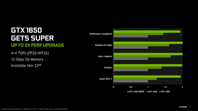
Like the other Super cards this year, the GTX 1650 Super is intended to be a mid-generation kicker for the GeForce family. However unlike the other Super cards, NVIDIA is giving the GTX 1650 Super a much bigger jump in performance. With a planned increase in GPU throughput of 46%, and paired with faster  12Gbps GDDR6 memory, the new card should be much farther ahead of the GTX 1650 than what we saw with today’s GTX 1660 Super launch, relatively speaking.


The single biggest change here is the GPU. While NVIDIA is calling the card a GTX 1650, in practice it’s more like a GTX 1660 LE; NVIDIA has brought in the larger, more powerful TU116 GPU from the GTX 1660 series to fill out this card. There are cost and power consequences to this, but the payoff is that it gives NVIDIA a lot more SMs and CUDA Cores to work with. Coupled with that is a small bump in clockspeeds, which pushes the on-paper shader/compute throughput numbers up by just over 46%.


Such a large jump in GPU throughput also requires a lot more memory bandwidth to feed the beast. As a result, just like the GTX 1660 Super, the GTX 1650 Super is getting the GDDR6 treatment as well. Here NVIDIA is using slightly lower (and lower power) 12Gbps GDDR6, which will be attached to the GPU via a neutered 128-bit memory bus. Still, this one change will give the GTX 1650 Super 50% more memory bandwidth than the vanilla GTX 1650, very close to its increase in shader throughput.


Do note, however, that not all aspects of the GPU are being scaled out to the same degree. In particular, the GTX 1650 Super will still only have 32 ROPs, with the rest of TU116’s ROPs getting cut off along with its spare memory channels. This means that while the GTX 1650 Super will have 46% more shader performance, it will only have 4% more ROP throughput for pushing pixels. Counterbalancing this to a degree will be the big jump in memory bandwidth, which will keep those 32 ROPs well-fed, but at the end of the day the GPU is getting an uneven increase in resources, and gaming performance gains are likely to reflect this.


The drawback to all of this, then, is power consumption. While the original GTX 1650 is a 75 Watt card – making it the fastest thing that can be powered solely by a PCIe slot – the Super-sized card will be a 100 Watt card. This gives up the original GTX 1650’s unique advantage, and it means builders looking for even faster 75W cards won’t get their wish, but it’s the power that pays the cost of the GTX 1650 Super’s higher performance. Traditionally, NVIDIA has held pretty steadfast at 75W for their xx50 cards, so I’ll be curious to see what this means for consumer interest and sales; but then again at the end of the day, despite the name, this is closer to a lightweight GTX 1660 than it is a GTX 1650.


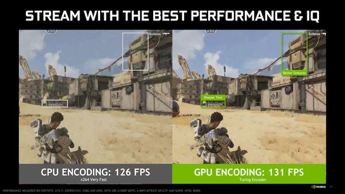
Speaking of hardware features, besides giving NVIDIA a good deal more in the way of GPU resources to play with, the switch from the TU117 GPU to the TU116 GPU will also have one other major ramification that some users will want to pay attention to: video encoding. Unlike TU117, which got the last-generation NVENC Volta video encoder block for die space reasons, TU116 gets the full-fat Turing NVENC video encoder block. Turing’s video encode block has been turning a lot of heads for its level of quality – while not archival grade, it’s competitive with x264 medium – which is important for streamers. This also led to TU117 and the GTX 1650 being a disappointment in some circles, as an otherwise solid video card was made far less useful for video encoding. So with the GTX 1650 Super, NVIDIA is resolving this in a roundabout way, thanks to the use of the more powerful TU116 GPU.


Moving on, the GTX 1650 Super is set to launch on November 22nd. And, while NVIDIA does not directly call out AMD in its production descriptions, the card’s configuration and timing makes a very compelling case that this is meant to be NVIDIA’s answer to AMD’s impending Radeon RX 5500. The first Navi 14-based video card is set to launch to retail sometime this quarter, and in their promotional material, AMD has been comparing it to the vanilla GTX 1650. So adding a GTX 1650 Super card allows NVIDIA to get ahead, in a fashion, by making available another (relatively) cheap card that, knowing NVIDIA, they expect to outperform what AMD has in the works. Of course the proof is in the pudding, so to speak, and at this point we’re waiting on both AMD and NVIDIA to actually launch their respective products before we can see how the competing cards actually stack up.


The other major wildcard here will be pricing. While NVIDIA is announcing the full specifications of the GTX 1650 Super today, they are withholding pricing information. This admittedly isn’t unusual for NVIDIA (they rarely release it more than a few days in advance), but in this case in particular, both NVIDIA and AMD seem to be playing a bit of a game of chicken. Neither side has announced where their card will be priced at, and it would seem that each is waiting on the other to go first so that they can counter with the best possible position for their respective card. Though with NVIDIA’s card not set to launch for another month, and AMD’s card more indeterminate still, we’re all going to be waiting for a while regardless.


At any rate, we’ll have more to talk about over the next month or so as the GTX 1650 Super and the rest of this holiday season’s video cards start hitting store shelves. So stay tuned.


Q4 2019 GPU Pricing Comparison
AMD Price NVIDIA
Radeon RX 5700 XT $399 GeForce RTX 2060 Super
Radeon RX 5700 $329 GeForce RTX 2060
  $279 GeForce GTX 1660 Ti
  $229 GeForce GTX 1660 Super
  $219 GeForce GTX 1660
Radeon RX 590 $199  
Radeon RX 580 $179  
Radeon RX 5500 ? GeForce GTX 1650 Super
  $149 GeForce GTX 1650


Source: AnandTech – NVIDIA Announces GeForce GTX 1650 Super: Launching November 22nd

The NVIDIA GeForce GTX 1660 Super Review, Feat. EVGA SC Ultra: Recalibrating The Mainstream Market

Kicking off the first of a series of video card launches for this holiday season is NVIDIA, who is announcing their GeForce GTX 1660 Super. This is a relatively minor, but none the less interesting revision to the GTX 1660 family that adds a 1660 (vanilla) SKU with faster GDDR6 memory for improved performance. Along with the GeForce GTX 1650 Super (shipping in late November), these two cards are going to be the backbone of NVIDIA’s mainstream efforts to close out the year. And while NVIDIA’s other GTX 1660 cards aren’t going anywhere, as we’re going to see today, with its $229 price tag, the GDDR6-equipped GTX 1660 Super is pretty much going to make the other 1660 cards redundant.


Source: AnandTech – The NVIDIA GeForce GTX 1660 Super Review, Feat. EVGA SC Ultra: Recalibrating The Mainstream Market

Apple Unveils AirPods Pro: A New Design with Active Noise Cancellation

Apple today has introduced a new version of its AirPods wireless earbuds, which the company is calling the AirPods Pro. Designed to be an even more premium version of Apple’s earbuds, the AirPods Pro features a revamped design that is equipped with a custom high dynamic range amplifier, as well as adding support for active noise cancellation. And with a price tag of $249, Apple’s high-end earbuds will carry a price premium to match its new premium features.


Apple’s AirPods Pro is based on the company’s H1 system-in-package, the same SiP that is used for the 2nd Generation AirPods introduced earlier this year. The new earbuds feature a new design with soft silicone ear tips (the company will ship AirPods Pro with three different tips) as well as new vent system that promises to minimize the discomfort of using the in-ear headphones. The earbuds come with a new custom high dynamic range amplifier, which is used to power a low-distortion speaker that can provide bass down to 20 Hz. Meanwhile, according to Apple the H1 SiP as well as the Adaptive EQ technology automatically tunes low- and mid-frequencies of the audio according to the shape of an individual’s ear.


The sweat and water resistant AirPods Pro comes with outward-facing and inward-facing microphones. These are able to detect external sounds, allowing the headset to support active noise cancellation. According to Apple, the AirPods sample the environment at 200Hz, allowing them to quickly respond to changes in outside noise. Meanwhile the new AirPods also add a new feature that Apple is calling transparency mode, which that allows the user to hear the environment around them while using the earbuds, essentially offering an option to reduce/eliminate the noise-blocking properties of the earbuds.


Meanwhile, the new AirPods also support an Ear Tip Fit Test, which can detect whether the headset has a good fit. And of course, the earbuds also fully support the usual AirPods features, including hands-free ‘Hey Siri’ functionality and everything that is derived from that.


Apple’s AirPods Pro can work for up to 4.5 hours on one charge with ANC or Transparency mode activated, or for up to 5 hours without them. Talk time of the new headset is 3.5 hours.


The new AirPods Pro are compatible with a variety of Apple’s devices running iOS 13.2 or later, iPadOS 13.2 or later, watchOS 6.1 or later, tvOS 13.2 or later, or macOS Catalina 10.15.1 or later.


Apple’s AirPods Pro with a wireless charging case will be available starting Wednesday, October 30 in the US and 25 other countries. In the US, the product will cost $249.


Related Reading:


Source: Apple


Source: AnandTech – Apple Unveils AirPods Pro: A New Design with Active Noise Cancellation

GlobalFoundries and TSMC Sign Broad Cross-Licensing Agreement, Dismiss Lawsuits

GlobalFoundries and TSMC have announced this afternoon that they have signed a broad cross-licensing agreement, ending all of their ongoing legal disputes. Under the terms of the deal, the two companies will license each other’s semiconductor-related patents granted so far, as well as any patents filed over the next 10 years.


Previously, GlobalFoundries has been accusing TSMC of patent infringement. At the time of the first lawsuit in August, TSMC said that the charges were baseless and that it would defend itself in court. In October, TSMC countersued its rival and, in turn, accused GlobalFoundries of infringing multiple patents. Now, less than a month after the countersuit, the two companies have agreed to sign a broad cross licensing agreement and dismiss all ongoing litigation.


According to the agreement, GlobalFoundries and TSMC cross-license to each other’s worldwide existing semiconductor patents, as well as any patents that are filed by the two companies in the next 10 years. Broadly speaking, GlobalFoundries and TSMC have thousands of semiconductor-related patents between them, some of which were originally granted to AMD and IBM.


Cross-licensing agreements are not uncommon in the high-tech world. Instead of fighting each other in expensive legal battles, companies with a broad portfolio of patents just sign cross-licensing agreements with peers, freeing them up to focus on innovating with their products rather than having to find ways to avoid infringing upon rivals’ patents.


Related Reading:


Source: GlobalFoundries/TSMC Press Release


Source: AnandTech – GlobalFoundries and TSMC Sign Broad Cross-Licensing Agreement, Dismiss Lawsuits

GlobalFoundries Teams Up with Singapore University for ReRAM Project

GlobalFoundries has announced that the company has teamed up with Singapore’s Nanyang Technological University and the National Research Foundation to develop resistive random access memory (ReRAM). The next-generation memory technology could ultimately pave the way for use as a very fast non-volatile high-capacity embedded cache. The project will take four years and will cost S$120 million ($88 million).


Under the terms of the agreement, the National Research Foundation will provide the necessary funding to Nanyang Technological University, which will spearhead the research. GlobalFoundries will support the project with its in-house manufacturing resources, just like it supports other universities on promising technologies, the company says.


Right now, GlobalFoundries (and other contract makers of semiconductors) use eFlash (embedded flash) for chips that need relatively high-capacity onboard storage. This technology has numerous limitations, such as endurance and performance when manufactured using today’s advanced logic technologies (i.e., sub-20nm nodes), which is something that is required of embedded memories. This is the main reason why GlobalFoundries and other chipmakers are looking at magneto resistive RAM (MRAM) to replace eFlash in future designs as it is considered the most durable non-volatile memory technology that exists today that can be made using contemporary logic fabrication processes.


MRAM relies on reading the magnetic anisotropy (orientation) of two ferromagnetic films separated by a thin barrier, and thus does not require an erase cycle before writing data, which makes it substantially faster than eFlash. Furthermore, its writing process requires a considerably lower amount of energy. On the flip side, MRAM’s density is relatively low, its magnetic anisotropy decreases at low temperatures, which makes it a no-option for numerous applications, but which is still very promising for the majority of use cases that do not involve low temperatures.


This brings researchers to ReRAM, which relies on changing the resistance across a dielectric material (from ‘0’ to ‘1’ or otherwise) by electrical current. The technology also doesn’t require an erase cycle, promises very high endurance, and — assuming that the right materials are used — can work at a wide range of temperatures. Meanwhile, alloys used for ReRAM should be very stable in general in a bid to survive millions of switches and retain data, even when memory cells are produced using ‘thin’ moden fabrication processes (e.g., GF’s 12LP or 12FDX). Finding the right substances for ReRAM will be the main topic of NTU’s research, whereas GlobalFoundries will have to find a cost-efficient way to produce the new type of memory at its facilities if the research is successful.


For years to come, GlobalFoundries (and its rivals) will use MRAM for a wide variety of applications as the technology is mature enough, fast enough, and durable enough. The company’s eMRAM implementation ‘integrates well’ with both FinFET and FD-SOI process technologies (although FinFET implementation is not yet ready), the company says, so expect it to be used widely. According to the foundry, it has multiple 22FDX eMRAM tape outs planned for 2019 and 2020.


GlobalFoundries is not standing still and is evaluating several eNVM technologies for its roadmap beyond 2020, including ReRAM. The company does not expect the research to come to fruition before 2021, but it certainly hopes that ReRAM will become another useful embedded memory technology.


It is noteworthy that companies like Western Digital are working on ReRAM-based storage class memory (SCM) to compete against Intel’s 3D XPoint and other SCM technologies. SCM-class ReRAM will have its differences when compared to embedded ReRAM that GlobalFoundries is particularly interested in, which once again shows that the technology could be applied very widely.


Related Reading:


Sources: GlobalFoundries, Crossbar, Everspin, ChannelNewsAsia


Source: AnandTech – GlobalFoundries Teams Up with Singapore University for ReRAM Project

The Intel Core i9-9990XE Review: All 14 Cores at 5.0 GHz

Within a few weeks, Intel is set to launch its most daring consumer desktop processor yet: the Core i9-9900KS, which offers eight cores all running at 5.0 GHz. There’s going to be a lot of buzz about this processor, but what people don’t know is that Intel already has an all 5.0 GHz processor, and it actually has 14 cores: the Core i9-9990XE. This ultra-rare thing isn’t sold to consumers – Intel only sells it to select partners, and even then it is only sold via an auction, once per quarter, with no warranty from Intel. How much would you pay for one? Well we got one to test.


Source: AnandTech – The Intel Core i9-9990XE Review: All 14 Cores at 5.0 GHz

Intel Q3 2019 Fab Update: 10nm Product Era Has Begun, 7nm On Track

After years of delays, Intel is finally shipping its 10 nm processors in high volume, and the company is preparing to fire up another fab to produce an even larger volume of 10nm products. Along with producing more of the company’s existing Ice Lake-U/Y products, Intel is also planning for server CPUs and GPUs as well, with Ice Lake-SP CPU as well as the DG1 GPU already up and running in Intel’s labs. Meanwhile, even farther out, Intel is eyeing 2021 for the rollout of its EUV-based 7nm process.


During its earnings call on Thursday, Intel said that so far 18 premium systems based on its 10th Generation Core (Ice Lake) processors have been formally introduced and 12 more are expected in 2019. Right now, the company produces all of its 10 nm CPUs in Hillsboro, Oregon and Kiryat Gat, Israel. Starting next quarter, the company expects 10 nm chips to also ship from its Chandler, Arizona, fab, which will increase supply of Ice Lake processors and will get Intel prepared for a broader use of the manufacturing process that had caused company a lot of troubles.


In addition to client Ice Lake CPUs and Agilex FPGAs that are currently shipping, Intel’s 10 nm portfolio includes datacenter-grade Xeon (Ice Lake-SP) processors due in the second half of 2020, discrete DG1 GPU(s), an AI inference accelerator, and a 5G base station SoC. One thing to keep in mind here is that Intel will use different iterations of its 10 nm technology to make different chips.


Here is what Bob Swan, CEO of Intel, said:


“The Intel 10 nm product era has begun and our new 10th Gen Core Ice Lake processors are leading the way. In Q3, we also shipped our first 10 nm Agilex FPGAs. In 2020, we will continue to expand our 10 nm portfolio with exciting new products including an AI inference accelerator, 5G base station SoC, Xeon CPUs for server storage and network, and a discrete GPU. This quarter we have achieved power on exit for our first discrete GPU DG1, an important milestone.”


The big news here is that Intel produced the first samples of its DG1 GPU back in Q3, which means that the company now has actual silicon to work with. The chip will undergo at least one more iteration before it will be ready to ship commercially, but it is a good sign that Intel’s A0 DG1 GPU could be turned on. If Intel wants to launch these GPUs in mid-2020, then this is the right window to begin working on actual silicon.


One of the key operational challenges that Intel faces today in regards of its 10 nm fabrication process are yields, as they thwarted the technology from going HVM (high volume manufacturing) for years. According to Intel, yields are improving ahead of expectations for both for client and datacenter CPUs, though the company did not disclose any numbers.


7nm Technology on Track, 5nm in Development


Meanwhile, with their 10 nm evolution roadmap set till 2021, Intel’s manufacturing technology teams are now focused on 7 nm and 5 nm processes. Along with their 10nm status update, in their earnings call Intel has re-iterated that its EUV-based 7 nm technology was on-track for HVM in 2021, and that development of its 5 nm node was proceeding as planned.


According to Intel, having learnt from its 10 nm fabrication process and how its problems harmed its roadmap, the company has radically changed its approach to development of manufacturing technologies and actual products. The company no longer sets ultra-ambitious goals for scaling each node, but attempts to find a right balance between performance, power, cost, and timing. Furthermore, the manufacturer no longer designs products for a particular process, but intends to use the most optimal one it has at the moment. Overall, Intel says that it intends to get back to its usual process technology cadence and introduce brand-new technologies every 2 to 2.5 years, and recapture its process leadership in the future.


Intel’s first product to be made using its 7 nm manufacturing technology is its ‘big’ GPU for high performance computing that is due in Q4 2021, two years after the launch of the 10 nm Ice Lake CPU. Intel says that its 7 nm process is well on-track and the product will be released as planned. While Intel also plans to use 7+ and 7++ technologies in 2022 and 2023, the company is already working on its 5 nm process and is currently ‘engineering’ it, which means that the path-finding stage has been passed and fundamental things like materials and transistor structures were set.


Here is what Bob Swan, CEO of Intel, told analysts and investors on Thursday:


“We are on track to launch our first 7 nm based product, a datacenter-focused discrete GPU, in 2021, two years after the launch of 10 nm [products]. We are also well down the engineering path on 5 nm.”


Related Reading:


Source: Intel


Source: AnandTech – Intel Q3 2019 Fab Update: 10nm Product Era Has Begun, 7nm On Track

My First Time Playing Minecraft, Ever: Testing The Ray Tracing Beta

Earlier this year at Gamescom, NVIDIA and Mojang showed off an early beta build of the popular game Minecraft with additional ray tracing features. Ray Tracing is a rendering technology that should in principle more accurately generate an environment, offering a more immersive experience. Throughout 2018 and 2019, NVIDIA has been a key proponent of bringing ray tracing acceleration hardware to the consumer market, and as the number of titles supporting NVIDIA’s ray tracing increases, the company believes that enabling popular titles like Minecraft is going to be key to promoting the technology (and driving hardware sales). NVIDIA UK offered some of the press a short hands-on with the Minecraft Beta, and it is actually my first proper Minecraft experience.


Source: AnandTech – My First Time Playing Minecraft, Ever: Testing The Ray Tracing Beta

Razer’s Raptor 27 Gaming Monitor Now Available: QHD with 144 Hz FreeSync & HDR400

Razer this week started sales of its unique Raptor 27 gaming display, which it first introduced earlier this year. The monitor packs numerous gaming-oriented features such as AMD’s FreeSync, and it comes in a one-of-a-kind stand that offers some relatively extreme tilt options, as well as programmable Razer Chroma RGB lighting on the bottom.


The Razer Raptor 27 is a non-glare 27-inch IPS display featuring a 2560×1440 resolution, a 420 nits peak luminance, a 1000:1 contrast ratio, a 144 Hz maximum refresh rate, and a 1 ms ULMB response time; all of which is fairly typical for an IPS QHD gaming monitor nowadays. A more unique feature of the Raptor 27 is its internal 10-bit dimming processor that, as its name suggests, controls the backlighting. The same processor seems to be responsible for managing the backlight’s total color gamut, allowing the monitor to cover 95% of the DCI-P3 color space, something that not all gaming LCDs can do.


Meanwhile, as a gaming monitor, the Raptor 27 supports AMD’s FreeSync variable refresh rate technology, and is also listed as NVIDIA G-Sync compatible. The monitor is also HDR capable, as the VESA DisplayHDR 400 badge will attest to, but like other DisplayHDR 400 monitors, only marginally so.


Meanwhile the chassis of the Raptor 27 sports ultra-thin 2.3-mm bezels on three sides, as well as a CNC-machined stand with integrated cable management. The stand can tilt all the way to 90º, providing easy access to display’s inputs.


Speaking of inputs, the Raptor 27 has a DisplayPort 1.4 input, an HDMI 2.0b port, and a USB Type-C port (with DP 1.4 alt-mode) that can also power a laptop. For peripherals, the monitor offers a dual port USB 3.0 Type-A hub, as well as a headphone jack.


The Razer Raptor 27 Gaming Display
  General Specifications
Display Size 27-inch
Panel Type IPS
Resolution 2560×1440
Refresh Rate 144 Hz with FreeSync
Response time 7ms typical

4ms Overdrive

1ms with Motion Blur Reduction
Contrast Ratio 1000:1
Brightness 420 nits
Color Gamut 95% DCI-P3
HDR DisplayHDR 400
Other 10-bit dimming processor
Connectivity 1 x HDMI 2.0

1 x DisplayPort 1.4

1 x USB Type-C with power delivery

1 x Headphone output

2 x USB 3.0
Availability October 2019
Price $699.99

Razor’s Raptor 27 monitor is hitting the streets at $699, which brings it in at the high-end of the prce range for 27-inch gaming displays with comparable characteristics.


Related Reading:


Source: Razer


Source: AnandTech – Razer’s Raptor 27 Gaming Monitor Now Available: QHD with 144 Hz FreeSync & HDR400

The ASUS ROG Crosshair VIII Impact: A Sharp $430 Impulse on X570

One of the most interesting unveilings from the X570 launch earlier this year came from ASUS, with the reintroduction of the ROG Impact series of small form factor motherboards. Not seen since the days of Intel Z170 days, the ASUS ROG Crosshair VIII Impact is the first truly AMD high-end SFF model from the vendor. Accompanied by its SO-DIMM.2 slot for dual PCIe 4.0 x4 M.2 SSDs, a SupremeFX S1220 HD audio codec and support for up to DDR4-4800 memory, the Impact looks to leave its mark on AM4 for enthusiasts just like previous iterations have done on Intel platforms. The only difference this time round is that it’s not a true Mini-ITX like the previous Impact designs.


Source: AnandTech – The ASUS ROG Crosshair VIII Impact: A Sharp 0 Impulse on X570

Intel Boosts 14nm Capacity 25% in 2019, But Shortages Will Persist in Q4

Higher-than-expected demand for Intel’s server and PC processors has been an interesting topic of discussion since the middle of 2018, when Intel first informed investors of its backlogged status. Since then, the situation has continued to dog the company, as executives have noted in virtually every quarterly conference call since that they haven’t been able to meet the demand that’s already pushed the company to record revenues. Since mid-2018, Intel has invested billions of dollars to increase its output of CPUs made using its 14 nm fabrication process, its most widely used technology these days. And yet even with that increase in 14nm capacity, the company expects that in the coming quarters they will contine to struggle.


The world’s largest supplier of processors boosted its 14 nm capacity in terms of wafer starts per month (WSPM) by 25% in 2019 as compared to 2018, Bob Swan, CEO of Intel, told analysts and investors during the company’s earnings conference call on Thursday. In the first three quarters of the year the firm spent $11.5 billion of CapEx money to buy new production equipment and now expects its total CapEx for the year to hit a whopping $16 billion, which is $0.5 billion higher than expected. Besides increasing its 14 nm capacity, Intel is also preparing to ramp up production of chips using its 10 nm technology, as well as start making enterprise-grade GPUs using its 7 nm process in 2021.


While the increase of the number of 14 nm wafer starts per month is a very good news – and Intel certainly deserves respect for the achievement – it’s worth noting that 25% more wafers does not necessarily mean 25% more CPUs. Demand for processors with a higher core count and a bigger die size means that Intel has to produce more wafers just to maintain the number of CPUs it can ship. It is hard to estimate whether or not a 25% WSPM increase is sufficient, but Intel itself says that in the fourth quarter the supply-demand balance for its PC customers will not be met, despite the fact that shipments of Intel’s CPUs will be up ‘double digits’ in the second half of the year compared to the first half of the year. 


Here is what the CEO of Intel had to say:


“We expect our second-half PC client supply will be up double-digits compared to the first-half. And we expect to further increase our PC client supply by mid-to-high single-digits in 2020. But that growth has not been sufficient. We are letting our customers down, and they are expecting more from us. PC demand has exceeded our expectations and surpassed third-party forecasts. We now think the market is stronger than we forecasted back in Q2, which has made building inventory buffers difficult. We are working hard to regain supply demand balance. But we expect to continue to be challenged in the fourth quarter.”


The company is looking forward to finally catching up to total demand in 2020 as it ramps up additional 14 nm capacity, but for now it will give priority to production of Xeon as well as advanced Core i5/i7/i9 processors.


Related Reading:


Source: Intel


Source: AnandTech – Intel Boosts 14nm Capacity 25% in 2019, But Shortages Will Persist in Q4

ASRock Unveils Three New X299 Motherboards For Cascade Lake-X

With Intel’s new Cascade Lake-X HEDT processors coming soon, ASRock has announced three new motherboards – the Steel Legend, the Creator, and the Taichi CLX. The trio is spearheaded by the high-end X299 Creator which is focused on content creators with features such as an Aquantia 10 gigabit Ethernet controller, Intel’s Wi-Fi 6, three PCIe 3.0 x4 M.2 slots, and a whopping 10 SATA ports. The ASRock X299 Creator also has an Intel Thunderbolt 3 chip for with 40 Gbps Type-C connectivity.


ASRock X299 Steel Legend


Starting out with the ASRock X299 Steel Legend, it has four full-length PCIe 3.0 slots which run at x16/x4/x16/x8, with a single PCIe 3.0 x1 slot. Storage capabilities consist of two PCIe 3.0 x4 M.2 slots which also support SATA drives, with a total of eight SATA ports with support for RAID 0, 1, 5 and 10 arrays. Each M.2 slot includes an M.2 heatshield to keep hot running NVMe SSDs cool. The eight memory slots allow users to use up to DDR4-4200 with a total supported capacity of up to 256 GB.


For the networking is a pair of Ethernet ports on the rear panel, one powered by an Intel I219 V, and the other by an Intel I211-AT Gigabit controller. Also on the rear panel is two USB 3.2 G2 20 Gbps Type-C ports from an ASMedia ASM3242 controller, three USB 3.1 G1 Type-A, and four USB 2.0 ports. The audio is powered by a Realtek ALC1220 HD audio codec which controls the five 3.5 mm audio jacks and S/PDIF optical output. The aesthetic also follows previous ASRock Steel Legend models with a silver and grey design, with RGB LEDs integrated into the X570 chipset heatsink. The ASRock X299 Steel Legend also uses an 11-phase power delivery with a large aluminium heatsink connected to the rear panel cover which designed to keep it cool.


ASRock X299 Taichi CLX


ASRock has redefined its fabled and unique Taichi design with the new X299 Taichi CLX. Firstly ASRock has gone with a black Taichi inspired PCIe cover which dominates the lower portion of the PCB. Incorporated into the design is a contrasting silver chipset heatsink with a gold and black cogwheel design with integrated RGB LEDs. The new ASRock X299 Taichi CLX is using a 13-phase power delivery with a heat pipe connecting the heatsink within the rear panel cover to the large aluminium power delivery heatsink. Like the ASRock X299 Steel Legend, the X299 Taichi CLX also features eight memory slots with support for up to DDR4-4200 and allows users to install up to 256 GB. Looking at PCIe support, there are four full-length PCIe 3.0 slots which operate at x16/x8/x16/x8, with a PCIe 3.0 x1 slot also present. 


The boards three PCIe 3.0 x4 M.2 slots share bandwidth with the second full-length slot and when populating a SATA based drive, the slot will operate at x4 mode, with an NVMe drive completely disabling this slot. A Realtek ALC1220 HD audio codec takes care of the boards onboard audio, while an assisting Texas Instruments NE5532 headset amplifier is present to bolster the quality of the front panel audio with support for headsets of up to 600 Ohms. A total of 10 SATA ports are present, with eight featuring support for RAID 0, 1, 5, and 10 arrays, while the other two ports are not controlled from the X299 chipset. Instead, these are powered by an ASMedia ASM1061 SATA controller. The networking consists of a Realtek RTL8125AG 2.5 Gigabit Ethernet controller, with a second port powered by an Intel I219-V Gigabit controller; the ASRock X299 Taichi CLX also includes an Intel AX200 Wi-Fi 6 wireless interface which also offers users with BT 5.0 connectivity.


ASRock X299 Creator


Finishing off with ASRock’s new flagship X299 motherboard, the X299 Creator, its focus is on content creators with a strong high-end feature set. The ASRock X299 Creator has an Aquantia AQC107 Ethernet controller with an assist going to an Intel I219-V Gigabit controller, with an Intel AX200 Wi-Fi 6 interface providing both Wi-Fi and BT 5.0 connectivity. There are four full-length PCIe 3.0 slots which operate at x16/x8/x16/x8, with three PCIe 3.0 M.2 slots, and a total of 10 SATA ports eight of those supporting RAID 0, 1, 5, and 10 arrays.


ASRock hasn’t unveiled the full specifications for the X299 Creator as of yet, and it’s not likely to be cheap based on the price of ASRock’s current flagship models. The ASRock X299 Creator, X299 Taichi CLX, and X299 Steel Legend models look set to be launched sometime in November, with no pricing information at present.


Confusing Naming Scheme: X299 Creator


One highly confusing aspect to ASRock’s new X299 Creator comes in the name Creator; MSI has already announced an X299 Creator model. It’s bad enough that Intel and AMD consistently make its chipset names similar such as B250 for Intel and B350/B450 for AMD which can confuse, and even mislead users. Both the ASRock X299 Creator and MSI X299 Creator focus the aim at the wallets of content creators, but both share the same model name which is sure to cause confusion among users. This is not only unacceptable in the modern market, it’s worth noting that MSI used to call its content creator series models the ‘Creation’, with ASRock unveiling its first Creator model on the X570 chipset. 


Related Reading


Source: AnandTech – ASRock Unveils Three New X299 Motherboards For Cascade Lake-X