Cloud Provider Gets $2.3 Billion Debt Using Nvidia's H100 as Collateral

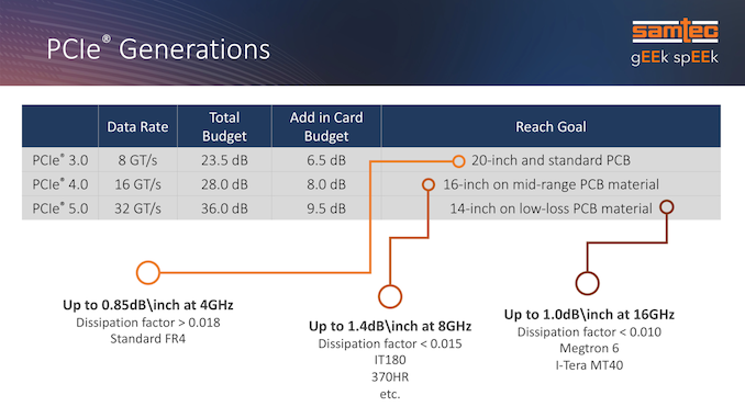
CoreWeave, an Nvidia-backed cloud service provider specializing in GPU-accelerated services, has secured a debt facility worth $2.3 billion using Nvidia’s H100-based hardware as collateral. The company intends to use the funds to procure more compute GPUs and systems from Nvidia, construct new data centers, and hire additional personnel to meet the growing needs for AI and HPC workloads.


CoreWeave has reaped enormous benefits from the rise in generative AI due to its large-scale cloud infrastructure as well as an exclusive relationship with Nvidia, and its ability to procure the company’s H100 compute GPUs as well as HGX H100 supercomputing platforms amid shortages of AI and HPC hardware. Since many AI and HPC applications used nowadays were developed for Nvidia’s CUDA platform and API, they require Nvidia’s GPUs. Therefore, access to H100 gives CoreWeave a competitive edge over traditional CSPs like AWS, Google, and Microsoft.


In addition to offering its customers access to advanced hardware, CoreWeave collaborates with AI startups and major CSPs — which are essentially its competitors — to build clusters that power AI workloads. These rivals — AWS and Google — have their own processors for AI workloads, and they continue to develop new ones. Still, given the dominance of CUDA, they have to offer Nvidia-powered instances to their clients and are currently grappling with Nvidia GPU supply limitations.


CoreWeave’s competitive advantage, facilitated by access to Nvidia’s latest hardware, is a key factor in the company’s ability to secure such substantial credit lines from companies like Magnetar Capital, Blackstone, Coatue, DigitalBridge, BlackRock, PIMCO, and Carlyle. Meanwhile, CoreWeave has already gotten $421 million from Magnetar at a valuation exceeding $2 billion.


Notably, this is not the first example of an Nvidia-supported startup reaping substantial benefits from its association with the tech giant. Last month, Inflection AI built a supercomputer worth hundreds of millions of dollars powered by 22,000 Nvidia H100 compute GPUs.


Meanwhile, this is the first time Nvidia’s H100-based hardware was used as collateral, emphasizing these processors’ importance in the capital-intensive AI and HPC cloud business. Moreover, this massive loan indicates the growing market for private asset-based financing secured by actual physical assets.


We negotiated with them to find a schedule for how much collateral to go into it, what the depreciation schedule was going to be versus the payoff schedule,” said Michael Intrator, CoreWeave’s CEO. “For us to go out and to borrow money against the asset base is a very cost-effective way to access the debt markets.”


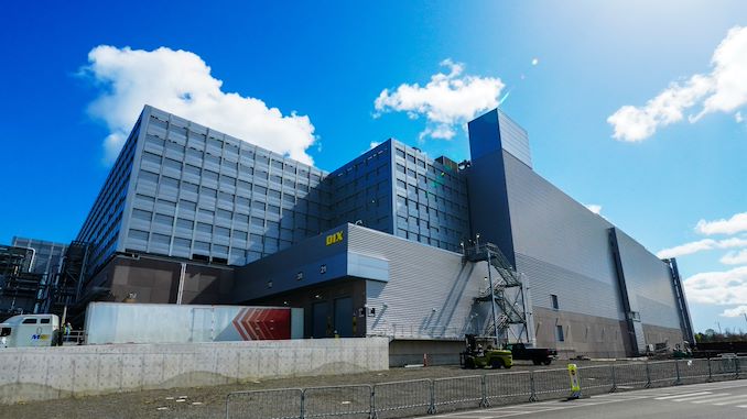
The company recently announced a $1.6 billion data center in Texas and plans to expand its presence to 14 locations within the U.S. by the end of 2023.


Source: Reuters


Source: AnandTech – Cloud Provider Gets .3 Billion Debt Using Nvidia’s H100 as Collateral

AMD to Introduce New Enthusiast-Class Graphics Cards This Quarter

As part of their quarterly earnings call this week, AMD revealed that the company is getting ready to launch new enthusiast-class Radeon RX 7000-series graphics cards in the coming months. To date, the company has launched cards for the top and bottom portions of their product stack, leaving a noticeable gap for higher performing cards that the company needs to fill to fully flesh out the current card lineup.


“We are on track to further expand our RDNA 3 GPU offerings with the launch of new, enthusiast-class Radeon 7000 series cards in the third quarter,” said Lisa Su, chief executive of AMD, at the company’s earnings call with analysts and investors.


So far, AMD has introduced four RDNA 3-based Radeon RX 7000-series desktop graphics cards aimed at diversified market segments: three Radeon RX 7900-series offerings for enthusiasts who can spend between $650 and $1000 on a graphics card, and the Radeon RX 7600 product for mainstream gamers at roughly $270. This has left an empty space for higher performing cards for cost-conscientious enthusiasts that, for the moment, is being met by NVIDIA’s GeForce RTX 4000-series as well as previous-generation Radeon RX 6000-series boards. In particular, AMD lacks currently lacks something current to compete with NVIDIA’s modestly well received GeForce RTX 4070.


AMD is believed to have only one GPU left in its Navi 30 range, Navi 32, which would slot in between the current Navi 31 and Navi 33 parts. Navi 32, in turn, is expected to power both Radeon RX 7700 and RX 7800 product families. That said, one thing that remains to be seen is whether the company will decide to go after volume first this quarter and start things off with the RX 7700 series, or after higher margins and reveal its Radeon RX 7800 series first.


AMD’s gaming segment revenue was $1.6 billion in Q2 2023, down 4% year-over-year and 10% sequentially primarily due to lower sales of gaming graphics cards. Unit sales of graphics processors in Q2 are typically lower than their shipments in Q1, so a 10% quarter-over-quarter decrease is not surprising. Meanwhile, a 4% drop YoY indicates that appeal of AMD’s discrete GPUs was lower in Q2 2023 compared to Q2 2022, an indicator that the company needs new products.


Source: AnandTech – AMD to Introduce New Enthusiast-Class Graphics Cards This Quarter

AMD Announces Radeon Pro W7600 & W7500: Pro RDNA 3 For The Mid-Range

As AMD continues to launch their full graphics product stacks based on their latest RDNA 3 architecture GPUs, the company is now preparing their next wave of professional cards under the Radeon Pro lineup. Following the launch of their high-end Radeon Pro W7900 and W7800 graphics cards back in the second quarter of this year, today the company is announcing the low-to-mid-range members of the Radeon Pro W7000 series: the Radeon Pro W7500 and Radeon Pro W7600. Both based on AMD’s monolithic Navi 33 silicon, the latest Radeon Pro parts will hit the shelves a bit later this quarter.

The two cards, as a whole, will make up what AMD defines as the mid-range segment of their professional video card market. And like their flagship counterparts, AMD is counting on a combination of RDNA 3’s advanced features, including AV1 encoding support, improved compute and ray tracing throughput, and DisplayPort 2.1 outputs to help drive sales of the new video cards. That, and as is tradition, significantly undercutting NVIDIA’s competing professional cards.


Source: AnandTech – AMD Announces Radeon Pro W7600 & W7500: Pro RDNA 3 For The Mid-Range

Intel Plans Massive Expansion in Oregon: D1X and D1A to Be Upgraded

Intel has filed a permit application that outlines significant expansion plans for its campus near Hillsboro, Oregon. According to filings submitted to state regulators, the tech giant’s ambitious proposals include a fourth expansion phase for the D1X research facility and an upgrade of the older D1A fab situated on the same 450-acre property.


The planned enhancements will take place at the company’s Gordon Moore Park (previously known as Ronler Acres) campus, according to a 1,100-page air-quality permit application submitted by Intel to the Oregon Department of Environmental Quality back in July. While the filings highlight Intel’s intention to upgrade its existing facilities and build some additional capacity, they do not contain a specific financial outline for these projects. Furthermore, they indicate Intel’s potential plans, not commitments. Meanwhile, if the scale is comparable to previous Oregon expansions, the total investment could reach billions.


The last upgrade, D1X’s third phase, cost $3 billion and added over one million square feet to the campus. The latest expansion could potentially exceed this, given that Intel plans not only to add a fourth phase to D1X but also to overhaul the 30-year-old D1A factory, add manufacturing support buildings, and implement other upgrades. Intel anticipates that the installation of new equipment could begin as early as 2025, with the completion of additional work slated for 2028.


So far, Intel has not formally announced any plans about its Oregon campus, but in May, its chief executive Pat Gelsinger already implied that he wants the site to grow big.


I would be reticent to constrain my dreams for how big it might be in the future,” Gelsinger said.


The Gordon Moore Park site currently houses five fabs: D1X, Intel’s flagship manufacturing process development facility; D1A, Intel’s development fab built in the 1980s; 10nm-capable D1B and D1C fabs; and 7nm-capable D1D fab. Intel is the largest corporate employer in Oregon, with 22,000 workers.


This proposed expansion represents a significant milestone, not just for Intel but for Oregon as well. While the investment may not match the tens of billions earmarked for new campuses in Arizona and Ohio, it would nonetheless constitute one of Oregon’s largest capital projects to date. This would likely result in the addition of hundreds or possibly thousands of new jobs to Intel’s workforce in the state, reaffirming Intel’s commitment to ongoing investment in its Oregon research endeavors.


Source: AnandTech – Intel Plans Massive Expansion in Oregon: D1X and D1A to Be Upgraded

PCI-SIG Forms Optical Workgroup – Lighting The Way To PCIe's Future

The PCI-Express interconnect standard may be going through some major changes in the coming years, based on a new announcement from the group responsible for the standard. The PCI-SIG is announcing this morning the formation of a PCIe Optical Workgroup, whose remit will be to work on enabling PCIe over optical interfaces. And while the group is still in its earliest of stages, the ramifications for the traditionally copper-bound standard could prove significant, as optical technology would bypass some increasingly stubborn limitations of copper signaling that traditional PCIe is soon approaching.


First released in the year 2000, PCI-Express was initially developed around the use of high-density edge connectors, which are still in use to this day. The PCIe Card Electromechanical specification (CEM) defines the PCIe add in card form factors in use for the last two decades, ranging from x1 to x16 connections.


But while the PCIe CEM has seen very little change over the years – in large part to ensure backward and forward compatibility – the signaling standard itself has undergone numerous speed upgrades. Including the latest PCIe 6.0 standard, the speed of a single PCIe lane has increased by 32-fold since 2000 – and the PCI-SIG will double that once more with PCIe 7.0 in 2025. As a result of increasing the amount of data transferred per pin by such a significant amount, the literal frequency band width used by the standard has increased by a similar degree, with PCIe 7.0 set to operate at nearly 32GHz.


In developing newer PCIe standards, the PCI-SIG has worked to minimize these issues, such as by employing alternative means of signaling that don’t require higher frequencies (e.g. PCIe 6 with PAM-4), and the use of mid-route retimers along with materials improvements have helped to keep up with the higher frequencies the standard does use. But the frequency limitations of copper traces within a PCB have never been eliminated entirely, which is why in more recent years the PCI-SIG has developed an official standard for PCIe over copper cabling.


Still in the works for late this year, the PCIe 5.0/6.0 cabling standard offers the option of using copper cables to carry PCIe both within a system (internal) and between systems (external). In particular, the relatively thick copper cables have less signal loss than PCB traces, overcoming the immediate drawback of high frequency comms, which is the low channel reach (i.e. short signal propagation distance). And while the cabling standard is designed to be an alternative to the PCIe CEM connector rather than a wholesale replacement, its existence underscores the problem at hand with high frequency signaling over copper, a problem that will only get even more challenging once PCIe 7.0 is made available.


PCIe Insertion Loss Budgets Over The Years (Samtec)


And that brings us to the formation of the PCI-SIG Optical Workgroup. Like the Ethernet community, which tends to be at the forefront of high frequency signaling innovation, PCI-SIG is looking towards optical, light-based communication as part of the future for PCIe. As we’ve already seen with optical networking technology, optical comms offers the potential for longer ranges and higher data rates vis-à-vis the vastly higher frequency of light, as well as a reduction in power consumed versus increasingly power-hungry copper transmission. For these reasons, the PCI-SIG is forming an Optical Workgroup to help develop the standards needed to supply PCIe over optical connections.


Strictly speaking, the creation of a new optical standard isn’t necessary to drive PCIe over optical connections. Several vendors already offer proprietary solutions, with a focus on external connectivity. But the creation of an optical standard aims to do just that – standardize how PCIe over fiber optics would work and behave. As part of the working group announcement, the traditionally consensus-based PCI-SIG is making it clear that they aren’t developing a standard for any single optical technology, but rather they are aiming to make it technology-agnostic, allowing the spec to support a wide range of optical technologies.


But the relatively broad announcement from the PCI-SIG doesn’t just stop with optical cabling as a replacement for current copper cabling, the group is also looking at “potentially developing technology-specific form factors.” While the classic CEM connector is unlikely to go away entirely any time soon – the backwards and forwards compatibility is that important – the CEM connector is the weakest/most difficult way to deliver PCIe today. So if the PCI-SIG is thinking about new form factors, then it’s likely the Optical Workgroup will at least be looking at some kind of optical-based successor to the CEM. And if that were to come to pass, this would easily be the biggest change in the PCIe specification in its 23+ year history.


But, to be sure, if any such change were to happen, it would be years down the line. The new Optical Workgroup has yet to form, let alone set its goals and requirements. With a broad remit to make PCIe more optical-friendly, any impact from the group is several years away – presumably no sooner than making a cabling standard for PCIe 7.0, if not a more direct impact on a PCIe 8.0 specification. But it shows where PCI-SIG leadership sees the future of the PCIe standard going, assuming they can get a consensus from their members. And, while not explicated stated in the PCI-SIG’s press release, any serious use of optical PCIe in this fashion would seem to be predicated on cheap optical transceivers, i.e. silicon photonics.


In any case, it will be interesting to see what eventually comes out of the PCI-SIG’s new Optical Workgroup. As PCIe begins to approach the practical limits of copper, the future of the industry’s standard peripheral interconnect may very well be to go towards the light.


Source: AnandTech – PCI-SIG Forms Optical Workgroup – Lighting The Way To PCIe’s Future

Intel Quietly Launches New Arc GPUs for Laptops

Intel has quietly released two new Arc Alchemist-series graphics processors for laptops. The new Arc A530M and Arc A570M target mid-range notebooks designed for light gaming. Perhaps the most intriguing thing about the new mobile GPUs is that they use previously unreleased ACM-G12 silicon.


Intel’s Arc A530M GPU comes with 12 Xe cores and 1536 stream processors operating at 1300 MHz, which clearly distinguishes it from the company’s entry-level Arc A370M GPU that only has eight Xe cores and 1024 stream processors. Meanwile, the Arc A570M features 16 Xe cores and 2048 stream processors running at 1300 MHz, which makes it clearly faster than the previously released Arc A550M with the same number of SPs at 900 MHz, but does not allow it to challenge the Arc A730M that has 3072 SPs working at 1100 MHz.


One interesting wrinkle about the Arc A530M and Arc A570M is that they seem to be based on Intel’s yet-to-be-confirmed ACM-G12 GPU, according to Bionic_Squash. This graphics processor reportedly has 16 Xe clusters, which means that it sits above the ACM-G11 with eight Xe clusters and Arc-G10 with 16 Xe clusters in total. Intel yet has to formally confirm that it uses its unannounced ACM-G12 silicon for the A530M and A570M parts.


Intel Arc Comparison
  Arc A370M Arc A530M Arc A550M Arc A570M Arc

A730M
Stream Processors 1024 1536 2048 2048 3072
Xe-cores 8 12 16 16 24
Render Slices 2 3 4 4 6
Ray Tracing Units 8 12 16 16 24
Xe Matrix Extensions (XMX) Engines 128 192 256 256 384
Xe Vector Engines 128 192 256 256 384
Graphics Clock 1550 MHz 1300 MHz 900 MHz 1300 MHz 1100 MHz
TGP 35-50W 65W-95W 60W 75W-95W 80W-120W
PCI Express  PCIe 4.0 x8 PCIe 4.0 x16
Memory Size 4 GB 4 GB

8 GB
8 GB 8 GB 12 GB
Memory Type GDDR6
Graphics Memory Interface 64 bit ? 128 bit ? 192 bit
Graphics Memory Bandwidth 112 GB/s ? 224 GB/s ? 336 GB/s
Graphics Memory Speed 14 Gbps ? 14 Gbps ? 14 Gbps


One of the things that strikes the eye about the new mobile GPUs is their thermal graphics power between 65W and 95W for the Arc A530M as well as between 75W and 95W for the Arc A570M. By contrast, the Arc A550M is rated for a 60W TGP, which makes it a considerably better choice than the Arc A530M both from performance and from battery life point of view.


What remains to be seen is whether Intel uses its ACM-G12 graphics processor for desktop parts too. While the company has formally announced its Arc A580 with 3072 stream processors, this part was based on the ACM-G10 and never came to market possibly because Intel did not want to address entry-level gaming market segment. It is unclear whether Intel is interested in rolling out a discrete desktop offering that would be positioned even below the unreleased Arc A580.


Intel’s newly released Arc A530M and Arc A570M are already supported by Intel’s latest graphics drivers.


Sources: Intel Ark (12), Bionic_Squash


Source: AnandTech – Intel Quietly Launches New Arc GPUs for Laptops

ASRock Z790 Taichi Carrara Motherboard Review: ASRock Rocks With White Marble

Building on the success of their hybrid architecture Alder Lake (12th Gen) Core series chips, Intel last year released the upgraded Raptor Lake core with a similar core architecture and design with performance (P) cores and efficiency (E) cores. While we’ve reviewed and put Intel’s 13th Gen Core series chips through their paces, it’s been a while since we tested out the platforms that not only unleash that multi-threaded and single-core IPC performance but add all of the features associated with each chipset. In a series of relative socket LGA 17000 motherboard reviews, we’re looking at perhaps one of the most interesting models for Intel’s 13th Gen Core series.

ASRock has added ‘Carrara’ to the mix, adding to their already popular Taichi series of motherboards that blend cogwheel-inspired aesthetics with a premium selection of controllers and features. Sometimes referred to as Luna marble by the Romans, the ASRock Z790 Taichi Carrara edition boasts a white Carrara marble-inspired design while retaining all the exact specifications and features of the regular Z790 Taichi. Some of the most prominent features include an advertised 27-phase (24+1+2) power delivery, support for DDR5-7400 memory, as well as dual Thunderbolt 4 Type-C ports on the rear panel.

ASRock loves to be different with its offerings, aka the Aqua series of motherboards. Still, the Taichi Carrara is different in that it celebrates ASRock’s 20th anniversary at the upper echelon of PC components and hardware. We take a closer look to see if the Z790 Taichi Carrara’s premium standing in ASRock’s Z790 line-up represents what we’ve come to like about the Taichi series over the years and, more importantly, how it performs against other LGA 1700 motherboards.


Source: AnandTech – ASRock Z790 Taichi Carrara Motherboard Review: ASRock Rocks With White Marble

China Imposes New Export Restrictions on Gallium and Germanium

China this week formally imposed new export regulations on gallium and germanium, as well as materials incorporating them. This move is broadly seen as a retaliatory act for the limitations recently placed on the Chinese semiconductor industry by the U.S., Japan, and the Netherlands. These new export regulations risk eventually significantly impacting the semiconductor sector, especially factories based in Japan.


Starting from August 1, 2023, Chinese companies are required to secure an export license to export gallium and germanium metals or any products that include these elements. With a stronghold over the global production of gallium (94%) and germanium (around 60%), China’s announcement of these restrictions in early July led to nearly a 20% price hike for gallium in the U.S and Europe. While the rules are said to be in the interests of China’s national security, many see them as a retaliation to curbs on China’s high-tech sector.


While the decision to restrict exports of gallium and germanium from China should not significantly impact the production of high-performance logic components like CPUs, GPUs, and memory, it is worth noting that GaN (gallium nitride) and GaAs (gallium arsenide) are integral to power chips, radio frequency amplifiers, LEDs, and numerous other applications.


Although gallium and germanium are not exceptionally rare and are typically acquired as byproducts of other mining operations, China’s dominance in their exports is due to its cheap refinement process, which made extracting these metals in other regions financially unviable. China’s new restrictions could cause an initial increase in prices and potential disruptions in supplies and component production. Yet, over time, these limitations may encourage companies from other countries to mine these metals, possibly threatening China’s market dominance. For example, Pentagon recently declared plans to recover gallium from waste electronics.


Japanese companies are likely to be the most affected by these new regulations, as Japan is the largest global consumer of gallium, based on data from the Japan Organization for Metals and Energy Security. Around 60% of gallium used in the country is imported, and China contributes 70% of these imports. Consequently, approximately 40% of Japan’s gallium supply is dependent on China.


Companies like Mitsubishi Chemical Group, which manufacture compound semiconductors and other products, reassure that they have adequate stocks in Japan to prevent any immediate supply issues. Other firms, including Sumitomo Chemical, a producer of gallium nitride substrates, and Nichia Corp., a producer of LEDs, also have plenty of gallium in stock, but are planning to monitor the situation and consider diversifying their suppliers. Meanwhile, to date, the new export rules have not affected Japanese companies’ raw material procurement or other business operations.


Despite the new rules, China’s Ministry of Commerce had stated that the export quality and quantity will remain unaffected. As long as exporters comply with national security protocols and other regulations, exports will continue as before. Meawhile, Wei Jianguo, ex-vice minister of commerce in China, cautions that the newly imposed export controls on gallium and germanium may only be the initial phase of China’s countermeasures. Looking ahead, China could potentially utilize its powerful position in specific commodity markets as a strategic means for exerting economic and diplomatic influence.


Source: Nikkei


Image Source: MIT


Source: AnandTech – China Imposes New Export Restrictions on Gallium and Germanium

Western Digital Preps 28 TB UltraSMR Hard Drive

Western Digital is gearing up to start sampling of its 28 TB nearline hard drive for hyperscalers. The new HDD will use the company’s energy-assisted perpendicular magnetic recording (ePMR) technology with UltraSMR track layouts. Since both technologies are now familiar to hyperscalers, the validation and qualification of this hard drive should be relatively straightforward.


“We are about to begin product sampling of our 28 TB UltraSMR drive,” said David Goeckeler, chief executive of Western Digital, at the company’s most recent earnings call. “This cutting-edge product is built upon the success of our ePMR and UltraSMR technologies with features and reliability trusted by our customers worldwide. We are staging this product for quick qualification and ramp as demand improves.”


Right now, Western Digital is shipping its 26 TB UltraSMR hard drives introduced over a year ago to select customers among operators of large cloud datacenters. Since these drives rely on UltraSMR it took hyperscalers quite a while to qualify them before deployment. But now that Western Digital’s customers know how to use UltraSMR and what to expect from it in terms of performance and behavior, deployment of 28 TB HDDs will likely go smoother.


Based on their release timeline, Western Digital’s 28 TB hard drives are expected to compete against Seagate’s 32 TB HDDs based on heat-assisted magnetic recording (HAMR) technology starting early 2024. Western Digital offering will be familiar to its clients who already use shingled magnetic recording HDDs in general and UltraSMR drives in particular. Meanwhile, Seagate’s product will deliver higher capacity, predictable performance (and considerably higher performance when it comes to write operations), but will probably need slightly longer qualification.


Western Digital’s UltraSMR set of technologies promises to add around 20% of extra capacity to CMR (conventional magnetic recording) platters. To make UltraSMR possible, Western Digital not only had to increase the number number of shingled bands and reduce the number of CMR bands, but employ all of its leading-edge HDD technologies. This includes triple stage actuators with two-dimensional (TDMR) read heads, ePMR write heads, OptiNAND technology, Distributed Sector (DSEC) technology and a proprietary error correcting code (ECC) technology with large block encoding to ensure that increased adjacent tracks interference (ATI) does not harm data integrity. In fact, the sophisticated ECC capability supported by an HDD controller may be crucial SMR hard drives in the coming years as well as for CMR drives in the longer-term future.


One interesting thing about Western Digital’s 28 TB HDD is that it will likely use the company’s 2nd generation ePMR since it is based on a 24 TB CMR drive and the latter is meant to rely on the ePMR 2 technology with advanced head structures, according to Western Digital’s roadmap.


Source: AnandTech – Western Digital Preps 28 TB UltraSMR Hard Drive

TeamGroup Unveils JEDEC-Spec DDR5-6400 Memory Kits: Faster 1.1V DDR5 On The Way For Future CPUs

While DDR5 memory has been out and in use for a couple of years now, so far we haven’t seen the memory reach its full potential – at least, not for rank-and-file standards-compliant DIMMs. The specification allows for speeds as high as DDR5-6400, but to date we’ve only seen on-spec kits (and processors) as fast as DDR5-5600. But at last, it looks like things are about to change and DDR5 is set to live up to its full potential, going by a new memory kit announcement from TeamGroup.


The memory kit vendor on Monday introduced its new ElitePlus-series DDR5-6400 memory modules, the first DDR5-6400 kit to be announced as JEDEC specification compliant. This means their new kit not only hits 6400 MT/s with standards-compliant timings, but arguably more importantly, it does so at DDR5’s standard voltage of 1.1V as well. And while there are no platforms on the market at this time that are validated for JEDEC DDR5-6400 speeds, TeamGroup’s product page already lists compatibility with Intel’s yet-to-be-announced “Z790 Refresh” platform – so suitable processors seem to be due soon.


TeamGroup’s Elite and ElitePlus DDR5-6400 memory modules come in 16 GB and 32 GB capacities (32 GB and 64 GB dual-channel kits) and feature JEDEC-standard CL52 52-52-103 timings as well as 1.1V voltage, as specified by the organization overseeing DRAM specs. For the moment, at least, TeamGroup’s DDR5-6400 modules are the industry’s fastest UDIMMs that are fully compliant with the JEDEC specifications.


And while DDR5-6400 speeds (and far higher) are available today with factory overclocked XMP/EXPO, the announcement of a JEDEC standards-compliant kit is still significant for a few different reasons. Being able to hit DDR5-6400B speeds and timings at 1.1V means DDR5 memory has improved to the point to make higher speeds at low voltages more viable, which has potential payoffs for memory at every speed grade by allowing for improved speeds and reduced power consumption/heat. And for OEM and other warrantied systems that only use JEDEC-complaint RAM, this allows for a straightforward improvement in memory speeds and bandwidth. About the only downside to faster on-spec kits is that they lack XMP or EXPO serial presence detect (SPD) profiles, which makes their configuration slightly more complicated on existing platforms from AMD and Intel, as they don’t officially support DDR5-6400. 


Meanwhile, on their product pages TeamGroup notes that the new RAM is compatible with Intel’s “Z790 Refresh” platform, a platform that has yet to be officially announced, but is rumored to go hand-in-hand with Intel “Raptor Lake Refresh” processors. Despite the lack of formal announcements from Intel there, TeamGroup seems to have let the cat out of the bag. So, prospective owners of Z790 Refresh systems can look forward to having access to specs-compliant 1.1V DDR5-6400 memory when that platform launches later this year.


As for the modules at hand, traditionally, TeamGroup’s Elite and ElitePlus memory modules are minimalistic and are aimed both at system integrators and at enthusiasts who are not after fancy designs of heat spreaders, RGB lighting, and maximum performance. In fact, TeamGroup’s Elite modules do not have heat spreaders at all, whereas ElitePlus modules have a minimalistic heat spreader that will not interfere with large CPU coolers.


TeamGroup says its Elite and ElitePlus DDR5-6400 memory modules will be available separately and in dual-channel kits starting from August in North America and Taiwan. And from that, we’d assume, Raptor Lake Refresh will not be far behind.


Source: AnandTech – TeamGroup Unveils JEDEC-Spec DDR5-6400 Memory Kits: Faster 1.1V DDR5 On The Way For Future CPUs

GEEKOM AS 6 (ASUS PN53) Review: Ryzen 9 6900HX Packs Punches in a Petite Package

The market demand for small form-factor (SFF) PCs was kickstarted by the Intel NUC in the early 2010s. Since then, many vendors have come out with their own take on the Intel NUC using both Intel and AMD processors. In recent years, we have also seen various Asian companies such as Beelink, Chuwi, GEEKOM, GMKtec, MinisForum, etc. emerging with a focus solely on these types of computing systems. Earlier this year, GEEKOM announced a tie-up with ASUS to market specific configurations of the ASUS ExpertCenter PN53 under their own brand as the GEEKOM AS 6. Based on AMD’s Rembrandt line of notebook processors, the GEEKOM AS 6 comes with a choice of Ryzen 9 6900HX, Ryzen 7 6800H, or the Ryzen 7 7735H. Read on for a detailed look at the performance profile and value proposition of the GEEKOM AS 6’s flagship configuration.


Source: AnandTech – GEEKOM AS 6 (ASUS PN53) Review: Ryzen 9 6900HX Packs Punches in a Petite Package

Dozens of Companies Adopt TSMC's 3nm Process Technology

Designing chips for modern, leading-edge manufacturing technologies is an expensive endeavor. Still, dozens of companies have already adopted TSMCs N3 and N3E (3 nm-class) fabrication processes, according to disclosures made by TSMC and Synopsys.


Synopsys IP for TSMC’s 3nm process has been adopted by dozens of leading companies to accelerate their development time, quickly achieve silicon success and speed their time to market,” said John Koeter, senior vice president of marketing and strategy for IP at Synopsys.


TSMC has been producing chips using its latest N3 (aka N3B) fabrication technology (with up to 25 EUV layers and support for EUV double patterning) since late 2022 and intends to start making products on its simplified N3E manufacturing process (with up to 19 EUV layers and without EUV double patterning) in Q4 2023. 


Previously, TSMC disclosed that its N3 nodes had been adopted by designers of high-performance computing (HPC) and smartphone SoCs and that the number of adopters was higher compared to N5 early in its lifecycle. Meanwhile, TSMC never mentioned the number of companies that had decided to use its 3 nm-class fabrication processes.


Synopsys is a major IP developer and electronic design automation tools provider, so it means a lot when it says that dozens of companies have licensed its IP for TSMC’s N3 fabrication technologies. But Synopsys is not the only IP designer out there, and companies like Cadence also supplied their N3-compatible IP to other fabless chip developers. It is safe to say that the number of their clients is also significant.


TSMC’s N3 family of process technologies includes baseline N3 (N3B), relaxed N3E with a bit reduced transistor density but widened process window for better yields, performance-enhanced N3P that is IP compatible with N3E will be production ready in the second half of 2024, and N3X for extremely high-performance applications that are due in 2025. 


The IP licensed by Synopsys right now can be used for N3, N3E, and N3P production nodes.


Sources: Synopsys


Source: AnandTech – Dozens of Companies Adopt TSMC’s 3nm Process Technology

Samsung Begins to Produce Third 3nm Chip Amid Massive Losses On DRAM & NAND

Samsung this week reported their financial results for the second quarter of 2023, closing the book on an especially bleak quarter of the year with a massive $3.4 billion operating loss. The losses, stemming from its semiconductor business, come amid a continued slump in 3D NAND and DRAM sales volumes and prices. Though buried deep in Samsung’s earnings report was a speck of good news, as well: the company has started to produce its third 3nm chip design with stable yield.


Discussing Samsung Foundry’s earnings, the company remains uncertain about demand recovery in the second half. “Demand to recover gradually under considerable uncertainty over the intensity of a market recovery in 2H, with consumer sentiment to rebound amid easing inflation and as customers wind down inventory adjustments,” a statement by Samsung reads.


More broadly, Samsung revenue dropped sharply, with the company recording a 22% year-over-year decline to $46.915 billion. Earnings of Samsung’s semiconductor divisions — including memory, SoCs, and foundry operations — declined to $29.86 billion, 48% YoY drop. Sales of memory hit $7 billion, a 57% year-over-year decline, though eking out a 1% quarter-over-quarter increase. Overall, Samsung recorded a $3.4 billion loss from its semiconductor operations due to low demand for commodity memory and declining commodity 3D NAND and DRAM prices.


But there were some bright spots in Samsung’s DRAM business, as well. Demand for high-performance high-density premium products like DDR5 modules and HBM memory increased, which helped to partly offset slow sales of commodity memory.


“Bit growth exceeded guidance as we expanded sales of server products while actively responding to rising demand for DDR5 and AI-use HBM,” Samsung said. “Demand for high-density/high-performance products stayed strong, driven by increased investments focusing on AI by major hyperscalers.”


While Samsung expects demand for memory to recover in the second half, the company is expecting to enact additional production cuts to further support memory prices.


“We expect to see a gradual recovery of the memory market in the second half of the year, but the pace of the market rebound is likely to depend on our macro variables,” said Jaejune Kim, executive vice president of memory division. “


Kim said that Samsung would be making further alterations to the output of some products, including 3D NAND.


“Production cuts across the industry are likely to continue in the second half, and demand is expected to gradually recover as clients continue to destock their (chip) inventory,” a statement by Samsung reads.


Finally, as noted earlier, as part of Samsung’s earnings report the company also revealed that it’s started production on its third 3nm (GAAFET) chip.


“Mass production of our third GAA product is going smoothly thanks to the stabilization of the 3nm process, and we are developing an improved process for 3nm as planned based on mass production experience with GAA,” a statement by Samsung reads.


It recently transpired that Samsung Foundry has been producing the Whatsminer M56S++ cryptocurrency mining ASIC on its SF3E node (formerly known as 3GAE, 3nm gate-all-around early) for some time. It turned out a bit later that there is PanSemi, another developer of cryptocurrency mining hardware, that uses Samsung’s SF3E to make its mining ASIC. Now, Samsung confirms that there is another customer that uses its latest production node, though the company isn’t disclosing any further details about the client or their chip.


Producing tiny cryptocurrency mining ASICs is a good way test a new fabrication process on a commercial application since even with a relatively high defect density, yields of such chips will likely be good enough to be viable. Meanwhile, Samsung Foundry’s SF3E process technology promises to increase performance and cut down power consumption of cryptocurrency mining ASICs (vs. similar chips made on previous-generation nodes) and these are exactly that targets that miners would like to hit to boost their earnings.


Sources: Samsung, Reuters, Nikkei, SeekingAlpha


Source: AnandTech – Samsung Begins to Produce Third 3nm Chip Amid Massive Losses On DRAM & NAND

Seagate Ships First Commercial HAMR Hard Drives

Seagate announced this week that it had begun the first commercial revenue shipments of its next-generation HAMR hard drives, which are being shipped out as part of Seagate’s latest Corvault storage systems. This commercialization marks an important milestone in the HDDs market, as heat-assisted magnetic recording (HAMR) is expected to enable hard drives with capacities of 50 TB and beyond. Meanwhile, HDDs employing perpendicular magnetic recording (PMR) and shingled magnetic recording (SMR) technologies are expected to remain on the market for the foreseeable future.


We shipped our first HAMR-based Corvault system for revenue as planned during the June quarter,” said Gianluca Romano, chief financial officer of Seagate, at the company’s earnings call. “We expect broader availability of these CORVAULT systems by the end of calendar 2023.


Seagate officially disclosed in early June that its first HAMR-based HDDs feature a 32 TB capacity and use a familiar 10-platter platform. Meanwhile, the company refrained from releasing specific capacity details of the HAMR hard drives used in these revenue Corvault systems.


Beyond Corvault systems, Seagate also shipped its HAMR-based hard drives to key customers among hyper scalers for testing and evaluation. Hyperscalers, due to their extensive storage requirements, are expected to benefit significantly from capacity points exceeding 30 TB. Though with the new technology at hand, as well as slightly higher power requirements for HAMR drives than standard PMR and SMR hard drives, the hyperscalers are also playing it safe and thoroughly validating the drives to ensure consistent performance.


Seagate’s initial 32 TB HAMR hard drives will use the company’s 10-platter platform, a system already proven and currently in use. Using an established platform, Seagate effectively mitigates numerous potential points of failure, potentially ensuring predictable production yield. This is smart, given the introduction of new media and write heads with its HAMR hard drives. The same 10-platter platform is expected to be used for 36 TB, 40 TB, and even larger-capacity hard drives in the future with as few alterations as possible.


[We are] delivering on our 30+ TB HAMR product development and qualification milestones, with volume ramp on track to begin in early calendar 2024,” said Dave Mosley, chief executive officer of Seagate.[…] Initial customer qualifications are progressing well. We are on track to begin volume ramp in early calendar 2024. We are also preparing qualifications with more customers, including testing for lower capacity drives targeting VIA and enterprise OEM workloads.


Even though high-volume production of HAMR hard drives is slated to begin in roughly half a year, Seagate also reaffirmed its plans for another generation of PMR and SMR hard drives during the call. These HDDs target customers not yet ready to switch to HAMR technology. 


According to Seagate, they plan to introduce 24TB+ drives featuring PMR technology with two-dimensional magnetic recording (TDMR) read heads and SMR+TDMR in the near future.


Development efforts on what may be our last PMR product are nearing completion and will extend drive capacities into the mid-to-upper 20TB range,” Mosley said.


Source: AnandTech – Seagate Ships First Commercial HAMR Hard Drives

AMD Announces Ryzen 9 7945HX3D: Ryzen Mobile Gets 3D V-Cache

For this year’s ChinaJoy expo, AMD is taking to the show to announce a new and very special mobile CPU for high-end, desktop replacement-class laptops: the Ryzen 9 7945HX3D, AMD’s first V-cache-equipped mobile CPU. Slated to launch on August 22nd, the new chip is set to break new ground for AMD in the mobile space, all the while giving gamers an even more potent CPU for high-end gaming laptops.


Based on AMD’s cutting-edge 3D V-Cache packaging technology, which places an additional slice of L3 cache on top of the existing L3 cache on the core complex die (CCD), the Ryzen 9 7945HX3D marks the first time AMD has brought their extended L3 cache technology to the mobile space. And like the Ryzen desktop parts already featuring this cache, such as the Ryzen 9 7950X3D, AMD’s aim is to offer buyers – and especially gamers – a top-end part that can offer even better performance in select classes of workloads that can take advantage of the additional cache.


The Ryzen 9 7945HX3D is joining AMD’s current lineup of desktop replacement-class mobile SKUs, the Ryzen 7045HX ‘Dragon Range’ series, as its new flagship mobile part. First introduced earlier this year, the AMD Ryzen 7045HX series is designed to offer desktop-grade hardware and desktop-like performance, marking the first time in the Zen era that AMD has offered its desktop silicon in a mobile chip. The entirety of the 7045HX series is based on repacked desktop silicon, and the new Ryzen 9 7945HX3D is no exception – for all practical purposes, we’re essentially looking at a mobilized version of AMD flagship desktop part, the Ryzen 9 7950X3D.


Source: AnandTech – AMD Announces Ryzen 9 7945HX3D: Ryzen Mobile Gets 3D V-Cache

Micron Publishes Updated DRAM Roadmap: 32 Gb DDR5 DRAMs, GDDR7, HBMNext

In addition to unveiling its first HBM3 memory products yesterday, Micron also published a fresh DRAM roadmap for its AI customers for the coming years. Being one of the world’s largest memory manufacturers, Micron has a lot of interesting things planned, including high-capacity DDR5 memory devices and modules, GDDR7 chips for graphics cards and other bandwidth-hungry devices, as well as HBMNext for artificial intelligence and high-performance computing applications.


32 Gb DDR5 ICs


We all love inexpensive high-capacity memory modules, and it looks like Micron has us covered. Sometimes in the late first half of 2024, the company plans to roll-out its first 32 Gb DDR5 memory dies, which will be produced on the company’s 1β (1-beta) manufacturing process. This is Micron’s latest process node and which does not use extreme ultraviolet lithography, but rather relies on multipatterning.


32 Gb DRAM dies will enable Micron to build 32 GB DDR5 modules using just eight memory devices on one side of the module. Such modules can be made today with Micron’s current 16 Gb dies, but this requires either placing 16 DRAM packages over both sides of a memory module – driving up production costs – or by placing two 16 Gb dies within a single DRAM package, which incurs its own costs due to the packaging required. 32 Gb ICs, by comparison, are easier to use, so 32 GB modules based on denser DRAM dies will eventually lead to lower costs compared to today’s 32 GB memory sticks.


But desktop matters aside, Micron’s initial focus with their higher density dies will be to build even higher capacity data center-class parts, including RDIMMs, MRDIMMs, and CXL modules. Current high performance AI models tend to be very large and memory constrained, so larger memory pools open the door both to even larger models, or in bringing down inference costs by being able to run additional instances on a single server.


For 2024, Micron is planning to release 128GB DDR5 modules based on these new dies. In addition, the company announced plans for 192+ GB and 256+ GB DDR5 modules for 2025, albeit without disclosing which chips these are set to use.


Meanwhile, Micron’s capacity-focused roadmap doesn’t have much to say about bandwidth. While it would be unusual for newer DRAM dies not to clock at least somewhat higher, memory manufacturers as a whole have not offered much guidance about future DDR5 memory speeds. Especially with MRDIMMs in the pipeline, the focus is more on gaining additional speed through parallelism, rather than running individual DRAM cells faster. Though with this roadmap in particular, it’s clear that Micron is more focused on promoting DDR5 capacity than promoting DDR5 performance.


GDDR7 in 1H 2024


Micron was the first larger memory maker to announce plans to roll out its GDDR7 memory in the first half of 2024. And following up on that, the new roadmap has the the company prepping 16 Gb and 24 Gb GDDR7 chips for late Q2 2024.


As with Samsung, Micron’s plans for their first generation GDDR7 modules do not have them reaching the spec’s highest transfer rates right away (36 GT/sec), and instead Micron is aiming for a more modest and practical 32 GT/sec. Which is still good enough to enable upwards of 50% greater bandwidth for next-generation graphics processors from AMD, Intel, and NVIDIA. And perhaps especially NVIDIA, since this roadmap also implies that we won’t be seeing a GDDR7X from Micron, meaning that for the first time since 2018, NVIDIA won’t have access to a specialty GDDR DRAM from Micron.


HBMNext in 2026


In addition to GDDR7, which will be used by graphics cards, game consoles, and lower-end high-bandwidth applications like accelerators and networking equipment, Micron is also working on the forthcoming generations of its HBM memory for heavy-duty artificial intelligence (AI) and high-performance computing (HPC) applications.


Micron expects its HBMNext (HBM4?) to be available in 36 GB and 64 GB capacities, which points to a variety of configurations, such as 12-Hi 24 Gb stacks (36 GB) or 16-Hi 32 Gb stacks (64 GB), though these are pure speculations at this point. As for performance, Micron is touting 1.5 TB/s – 2+ TB/s of bandwidth per stack, which points to data transfer rates in excess of 11.5 GT/s/pin.


Source: AnandTech – Micron Publishes Updated DRAM Roadmap: 32 Gb DDR5 DRAMs, GDDR7, HBMNext

Rapidus Wants to Supply 2nm Chips to Tech Giants, Challenge TSMC

It has been a couple of decades since a Japanese fab has offered a leading-edge chip manufacturing process. Even to this day, none of the Japanese chipmakers have made it as far as adopting FinFETs, something that U.S. and Taiwanese companies adopted in early-to-mid-2010s. But Rapidus, a semiconductor consortium backed by the Japanese government and large conglomerates, plans to leapfrog several generations of nodes and start 2nm production in 2027. Interestingly, the company aims to serve world’s leading tech giants, challenging TSMC, IFS, and Samsung Foundry.


The endeavor is both extremely challenging and tremendously expensive. Modern fabrication technologies are expensive to develop in general. To cut down its R&D costs, Rapidus teamed up with IBM, which has done extensive research in such fields as transistor structures as well as chip materials. But in addition to developing a viable 2nm fabrication process, Rapidus will also have to build a modern semiconductor fabrication facility, which is an expensive venture. Rapidus itself projects that it will need approximately $35 billion to initiate pilot 2nm chip production in 2025, and then bring that to high-volume manufacturing in 2027.


To recover the massive R&D and fab construction costs, Rapidus will need to produce its 2nm chips in very high volumes. As demand from Japanese companies alone may not suffice, Rapidus is looking for orders from international corporations like Apple, Google, and Meta.


“We are looking for a U.S. partner, and we have begun discussions with some GAFAM [Google, Apple, Facebook, Amazon and Microsoft] corporations,” Atsuyoshi Koike, chief executive of Rapidus, told Nikkei. “Specifically, there is demand [for chips] from data centers [and] right now, TSMC is the only company that can make the semiconductors they envision. That is where Rapidus will enter.”


Despite escalating chip design costs, the number of companies opting to develop their own custom system-on-chips for artificial intelligence (AI) and high-performance computing (HPC) applications is growing these days. Hyperscalers like AWS, Google, and Facebook have already developed numerous chips in-house to replace off-the-shelf offerings from companies like AMD, Intel, and NVIDIA with something that suits them better.


These companies typically rely on TSMC since the latter tends to offer competitive nodes, predictable yields, and the ability to re-use IP across various products. So securing orders from a tech giant is challenging for a new kid on the block. But Rapidus’ strategy is not completely unfounded, as the number of hyperscalers that need custom silicon is growing and one or two may opt for Rapidus if the Japanese company can provide competitive technology, high yields, and fair pricing.


With that said, however, Rapidus is also making it clear that the company does not plan to emulate TSMC’s entire business model, where they’d serve a wide range of clients like TSMC does. Instead, Rapidus intends to start with about five customers, then gradually expand to 10, and then see if it wants and can serve more.


“Our business model is not that of TSMC, which manufactures for every client,” said Koike. “We will start with around five companies at most, then eventually grow to 10 companies, and we’ll see if we’ll increase the number beyond that.”


It is unclear whether such a limited client base can generate enough demand and revenue to recover Rapidus’ massive investment needed to kick-start 2nm production by 2027. It is also going to be a challenge to secure even five significant 2nm orders by 2027 given the limited number of companies ready to invest in chips to be made on a leading-edge technology and competition from established players like TSMC, Samsung Foundry, and IFS.


However, from the Japanese government’s perspective, Rapidus is seen as a catalyst for revitalizing Japan’s advanced semiconductor supply chain, rather than a money making machine in and of itself. So even if the 2nm project was not an immediate success, it can be justified as a stepping stone towards creating more opportunities for local chip designers.


As for revenue, Koike predicts that quotes for its 2nm chips will be 10 times greater than for chips currently made by Japanese firms, which is of course a significant change for the Japanese chip industry. This is not particularly surprising though, as the most advanced process technology available in Japan today is 45nm, which these days is a very inexpensive node as it is used on fully depreciated fabs and does not require any new equipment.


Sources: NikkeiDigiTimes


Source: AnandTech – Rapidus Wants to Supply 2nm Chips to Tech Giants, Challenge TSMC

Micron Unveils HBM3 Gen2 Memory: 1.2 TB/sec Memory Stacks For HPC and AI Processors

Micron today is introducing its first HBM3 memory products, becoming the latest of the major memory manufacturers to start building the high bandwidth memory that’s widely used in server-grade GPUs and other high-end processors. Aiming to make up for lost time against its Korean rivals, Micron intends to essentially skip “vanilla” HBM3 and move straight on to even higher bandwidth versions of the memory they’re dubbing “HBM3 Gen2”, developing 24 GB stacks that run at over 9 GigaTransfers-per-second. These new HBM3 memory stacks from Micron will target primarily AI and HPC datacenter, with mass production kicking off for Micron in early 2024.


Micron’s 24 GB HBM3 Gen2 modules are based on stacking eight 24Gbit memory dies made using the company’s 1β (1-beta) fabrication process. Notably, Micron is the first of the memory vendors to announce plans to build HBM3 memory with these higher-density dies, while SK hynix offers their own 24 GB stacks, the company is using a 12-Hi configuration of 16Gbit dies. So Micron is on track to be the first vendor to offer 24 GB HBM3 modules in the more typical 8-Hi configuration. And Micron is not going to stop at 8-Hi 24Gbit-based HBM3 Gen2 modules, either, with the company saying that they plan to introduce even higher capacity class-leading 36 GB 12-Hi HBM3 Gen2 stacks next year.


Besides taking the lead in density, Micron is also looking to take a lead in speed. The company expects its HBM3 Gen2 parts to hit date rates as high as 9.2 GT/second, 44% higher than the top speed grade of the base HBM3 specification, and 15% faster than the 8 GT/second target for SK hynix’s rival HBM3E memory. The increased data transfer rate enables each 24 GB memory module to offer peak bandwidth of 1.2 TB/sec per stack.


Micron says that 24GB HBM3 Gen2 stacks will enable 4096-bit HBM3 memory subsystems with a bandwidth of 4.8 TB/s and 6096-bit HBM3 memory subsystems with a bandwidth of 7.2 TB/s. To put the numbers into context, Nvidia’s H100 SXM features a peak memory bandwidth of 3.35 TB/s.


HBM Memory Comparison
  “HBM3 Gen2” HBM3 HBM2E HBM2
Max Capacity 24 GB 24 GB 16 GB 8 GB
Max Bandwidth Per Pin 9.2 GT/s 6.4 GT/s 3.6 GT/s 2.0 GT/s
Number of DRAM ICs per Stack 8 12 8 8
Effective Bus Width 1024-bit
Voltage 1.1 V? 1.1 V 1.2 V 1.2 V
Bandwidth per Stack 1.2 TB/s 819.2 GB/s 460.8 GB/s 256 GB/s


High frequencies aside, Micron’s HBM3 Gen2 stacks are otherwise drop-in compatible with current HBM3-compliant applications (e.g., compute GPUs, CPUs, FPGAs, accelerators). So device manufacturers will finally have the option of tapping Micron as an HBM3 memory supplier as well, pending the usual qualification checks.


Under the hood, Micron’s goal to jump into an immediate performance leadership position within the HBM3 market means that they need to one-up their competition from a technical level. Among other changes and innovations to accomplish that, the company increased the number of through-silicon vias (TSVs) by two times compared to shipping HBM3 products. In addition, Micron shrunk the distance between DRAM devices in its HBM3 Gen2 stacks. These two changes to packaging reduced thermal impendence of these memory modules and made it easier to cool them down. Yet, the increased number of TSVs can bring other advantages too.


Given that Micron uses 24 Gb memory devices (rather than 16 Gb memory devices) for its HBM3 Gen2 stacks, it is inevitable that it had to increase the number of TSVs to ensure proper connectivity. Yet, doubling the number of TSVs in an HBM stack can enhance overall bandwidth (and shrink latency), power efficiency, and scalability by facilitating more parallel data transfers. It also improves reliability by mitigating the impact of single TSV failures through data rerouting. However, these benefits come with challenges such as increased manufacturing complexity and increased potential for higher defect rates (already an ongoing concern for HBM), which can translate to higher costs.


Just like other HBM3 memory modules, Micron’s HBM3 Gen2 stacks feature Reed-Solomon on-die ECC, soft repair of memory cells, hard-repair of memory cells as well as auto error check and scrub support.


Micron says it will mass produce its 24 GB HBM3 modules starting in Q1 2024, and will start sampling its 12-Hi 36GB HBM3 stacks around this time as well. The latter will enter high volume production in the second half of 2024.


To date, the JEDEC has yet to approve a post-6.4GT/second HBM3 standard. So Micron’s HBM3 Gen2 memory, as well as SK hynix’s rival HBM3E memory, are both off-roadmap standards for the moment. Given the interest in higher bandwidth HBM memory and the need for standardization, we’d be surprised if the group didn’t eventually release an updated version of the HBM3 standard that Micron’s devices will conform to. Though as the group tends to shy away from naming battles (“HBM2E” was never a canonical product name for faster HBM2, despite its wide use), it’s anyone’s guess how this latest kerfuffle over naming will play out.


Beyond their forthcoming HBM3 Gen2 products, Micron is also making it known that the company already working on HBMNext (HBM4?) memory. That iteration of HBM will provide 1.5 TB/s – 2+ TB/s of bandwidth per stack with capacities ranging from 36 GB to 64 GB.


Source: AnandTech – Micron Unveils HBM3 Gen2 Memory: 1.2 TB/sec Memory Stacks For HPC and AI Processors

The Be Quiet! Dark Power Pro 13 1300W ATX 3.0 PSU Review: Flagship Quality, Flagship Price

Having reviewed and dissected almost a dozen ATX 3.0 power supplies in the last year, thus far we’ve seen an interesting mix in design pedigrees for PSUs targeting the newest power standard. For some manufacturers this has meant bringing up entirely new PSU designs by OEMs new and old, developing fresh platforms to accommodate the new 12VHPWR connector and its up to 600 Watt power limits. Meanwhile for other manufacturers, especially at the high end of the market, their existing PSU designs are so bulletproof that they’ve been able to add everything needed for ATX 3.0 compliance with only very modest changes.

For Be Quiet’s flagship power supply lineup, the Dark Power Pro series, the company falls distinctly in to the second group. The pride and joy of Be Quiet!’s lineup has always been the pinnacle of the company’s engineering abilities, with the best possible specifications their engineers could muster (and equally prodigious price tags for the consumer). Besides making for long-lived PSUs themselves, that kind of engineering rigor has also allowed for a long-lived platform – even with the more extreme power delivery requirements brought about by ATX 3.0, Be Quiet has only needed to make a handful of changes to meet the new standard.

The result of those updates is the latest generation of the Dark Power Pro series, the Dark Power Pro 13, which we’re looking at today. The 13th iteration of Be Quiet’s lead PSU series builds upon their already impressive design for the Dark Power Pro 12, adding compliance with Intel’s ATX 3.0 design guide while retaining the 80Plus Titanium certification and impressive features of the previous version.


Source: AnandTech – The Be Quiet! Dark Power Pro 13 1300W ATX 3.0 PSU Review: Flagship Quality, Flagship Price

TACC's Stampede3 Supercomputer Uses Intel's Xeon Max with HBM2E and Ponte Vecchio

The Texas Advanced Computing Center (TACC) unveiled its latest Stampede supercomputer for open science research projects, Stampede3. TACC anticipates that Stampede3 will come online this fall and will deliver its full performance in early 2024. The supercomputer will be a crucial component of the U.S. National Science Foundation’s (NSF) ACCESS scientific supercomputing ecosystem, and it is projected to serve the open science community from 2024 until 2029.


The third-generation Stampede cluster, which will be built by Dell, will incorporate 560 nodes equipped with Intel’s Sapphire Rapids generation Xeon CPU Max processors, each offering 56 CPU cores and 64GB of on-package HBM2E memory. Surprisingly, TACC is going to be operating these nodes in HBM-only mode, so no additional DRAM will be attached to the CPU nodes – all of their memory will come from the on-chip HBM stacks.


With these specifications, Stampede3 is expected to have a peak performance of approximately 4 FP64 PetaFLOPS, while offering nearly 63,000 general-purpose cores. In addition, TACC also plans to install 10 Dell PowerEdge XE9640 servers with 40 Intel Data Center GPU Max compute GPUs for artificial intelligence and machine learning workloads.


Given this layout, the bulk of Stampede3’s compute performance will be supplied by CPUs. This makes Stampede3 a bit of a rarity in this day and age, as most high-performance systems are GPU driven, leaving Stampede3 as one of the last supercomputers that relies almost solely on general-purpose CPUs.


And while the current cluster is primarily focused on CPU performance, TACC is also going to use the Intel GPUs in the latest Stampede revamp to investigate on how to incorporate larger numbers of GPUs into future versions of the system. For now, most of TACC’s AI tasks are run on its Lone Star systems, which is powered by hundreds Nvidia A100 compute GPUs. So the organization’s aim is to explore whether a portion of this workload can be transferred to Intel’s Ponte Vecchio.


We are going to put in a small system with exploratory capability using Intel Ponte Vecchio,” said Dan Stanzione, executive director of TACC. “We are still negotiating exactly how much of that will have, but I would say a minimum of 40 nodes and maximum of a hundred or so. […] We are just putting a couple of racks of Ponte Vecchio out there to see how people work with it.”


Stampede3 will leverage 400 Gb/s Omni-Path Fabric technology that will enable a backplane bandwidth of 24TB/s. This setup will allow the machine to efficiently scale and minimize latencies, making it well-suited for various applications requiring simulations.


TACC also plans to reincorporate nodes from the previous version, Stampede2, which were based on older-generation Xeon Scalable CPUs. This integration will enhance the capacity of Stampede3 for high-memory applications, high-throughput computing, interactive workloads, and other previous-generation applications. In total, the new supercomputer system will feature 1,858 compute nodes with over 140,000 cores, more than 330 TBs of RAM, new storage capacity of 13 PBs, and a peak performance close to 10 PetaFLOPS.


Sources: TACC, HPCWire


Source: AnandTech – TACC’s Stampede3 Supercomputer Uses Intel’s Xeon Max with HBM2E and Ponte Vecchio