Crucial X9 Pro Portable SSD Review: Micron 176L 3D NAND Delivers Record UFD Consistency

Crucial introduced their X9 Pro and X10 Pro high-performance portable SSDs last month. Based on Silicon Motion’s SM2320 native USB flash controller, coupled with Micron’s 176L 3D TLC NAND, these SSDs promise performance suitable for power users. The company sent across their 1 GBps-class X9 Pro for review first, followed by the X10 Pro a few weeks later. This review takes an in-depth look at the performance and value proposition of the X9 Pro and how it compares against other 1 GBps-class portable SSDs.


Source: AnandTech – Crucial X9 Pro Portable SSD Review: Micron 176L 3D NAND Delivers Record UFD Consistency

AMD to Unveil 'Major' New Radeon Products Next Week at Gamescom

Earlier this month, AMD said that it would refresh its lineup of Radeon RX graphics cards for gamers this quarter, and apparently, the new products are set to be announced next week at Gamescom in Cologne, Germany.


Please join the @AMDRadeon team at Gamescom next week for our next major product announcements,” said Scott Herkelman, senior vice president and general manager graphics business unit at AMD, in an X post


Frank Azor, chief architect of gaming solutions and marketing at AMD, linked Herkelman’s post and reaffirmed that the company has ‘some news coming next week.’


Indeed, Gamescom is a good place to announce new products. The trade show traditionally attracts hundreds of thousands of visitors, making it one of the biggest gaming events in the world. The fair is aimed at the general public and industry professionals. The event is split between an Entertainment Area for the public, where fans can try out upcoming games, and a Business Area for trade visitors to communicate and conduct deals. AMD plans to hold its AMD Gaming Festival 2023 on Friday, August 25, at Hall 7, which starts at 12:00.


While AMD does not disclose what exactly it plans to announce at Gamescom, it is about time for AMD to fill a gap in its Radeon RX 7000-series product line that spans from the Radeon RX 7600 ($270) and goes all the way to the Radeon RX 7900 XT ($900). This void is currently being filled by the older Radeon RX 6000-series and the Radeon RX 7900 GRE ($650), which is hard to get. Essentially, AMD does not have a direct answer to NVIDIA’s reasonably popular GeForce RTX 4070 at the moment.


It’s speculated that AMD’s next move is to unveil the Navi 32, a GPU from its RDNA 3-based lineup which would position itself between the existing Navi 31 and Navi 33 GPUs. AMD’s Navi 32 is anticipated to be the foundation for the Radeon RX 7700 and Radeon RX 7800 series, which will compete against Nvidia’s performance mainstream and higher-end GeForce RTX 40-series products.


Source: AnandTech – AMD to Unveil ‘Major’ New Radeon Products Next Week at Gamescom

Intel Calls Off Tower Acquisition, Forced to Focus Solely on Leading-Edge Nodes

Intel Corp. will not proceed with its $5.4 billion deal to acquire Tower Semiconductor foundry due to a lack of regulatory approval from China, the two companies announced on Wednesday. Instead of renegotiating, Intel will pay Tower a $353 million break-up fee to walk away. The move will force Intel to focus the business strategy of its Intel Foundry Services (IFS) division solely on leading-edge process technologies.


Good Fit


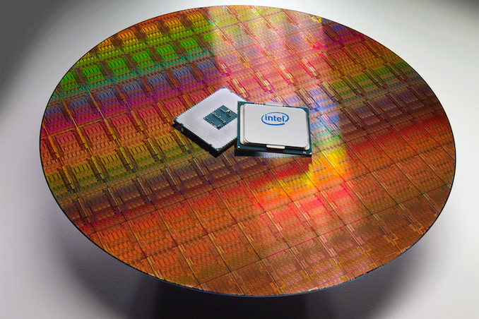
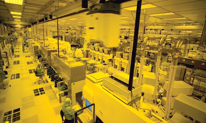
Intel’s business strategy has always relied on building leading-edge and producing the world’s most advanced chips on the most sophisticated production nodes to depreciate fabs while earning hefty margins quickly. As costs of modern fabs got inherently higher than they used to be and R&D costs of process technologies were consistently increasing, Intel needed to expand its production volumes to retain profitability, and offering foundry services was an excellent way to do so. 


Since Intel has historically only produced chips for itself, it tailored its process technologies solely for its CPU products. It had to outsource its own GPU and FPGA products manufacturing to TSMC or GlobalFoundries as their technologies were better fit for these types of devices. As a foundry, Intel needed to tailor its nodes for a broader range of applications (which it presumably did with 20A and 18A) and ensure compatibility of its process technologies with commercially available electronic design automation (EDA) and verification tools. But Intel also needed to offer something more than just leading-edge nodes for the most sophisticated chips on the planet.


So, it decided to acquire another contracted chip maker, and Tower Semiconductor seemed like a good fit. Tower’s expertise lies in manufacturing specialized chips, such as mixed-signal, RFCMOS, silicon photonics, PMICs, and more, using specialty and mature process technologies like BiCMOS, SiGe, and SOI at its seven fabs in Israel, the U.S., and Japan. These technologies might not be at the forefront of innovation. Still, they are crucial for applications that are made in huge volumes, have very long lifecycles, and are always in high demand. Therefore, the deal would significantly expand IFS’s client base in the foundry sector and bring onboard experts with vast experience in contract chipmaking.


Re-Focusing Solely to Leading-Edge Nodes


Without Tower, IFS will need to focus on making chips on just a few nodes (Intel 1620A, 18A, and Intel 3) and will compete directly with TSMC and Samsung Foundry using only these process technologies. Instead of gaining dozens of customers overnight, IFS will have to work hard to land orders and grow its customer base. Still, the company says it is not dropping its plan to become the world’s second-largest foundry by 2030, thus replacing Samsung from the No. 2 spot.


Since its launch in 2021, Intel Foundry Services has gained traction with customers and partners, and we have made significant advancements toward our goal of becoming the second-largest global external foundry by the end of the decade,” said Stuart Pann, senior vice president and general manager of Intel Foundry Services (IFS). 


This is not going to be particularly easy. IFS’s journey has been filled with ups and downs. IFS’s partnerships with Arm, MediaTek, and the U.S. Department of Defense highlight its growing influence in the sector. Furthermore, Intel’s commitment to building leading-edge fabs and advanced packaging facilities in different parts of the world (Europe, Middle East, North America) emphasizes that the company is looking for clients across the globe and is no longer focused entirely on its own products.


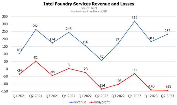
However, the financial side tells a different story. In 2021, Intel’s foundry unit reported revenues of $786 million but faced a loss of $23 million. The following year it reported revenues of $703 million (after adjusting its financial statements for the first two quarters of 2022) and a loss of $291 million. In 2023, IFS has seen revenues of $415 million, marking a 13% increase from the first half of 2021 and a 94% jump from the first half of 2022, but it also reported a loss of $283 million. 


By contrast, Tower Semiconductor reported revenue of $1.68 billion in 2022, up from $1.51 billion in 2021. The company’s net profit for 2022 reached $265 million, a 76% surge compared to the $150 million recorded in 2021.


Furthermore, two years since the formal establishment of IFS, only MediaTek has officially committed to using Intel’s advanced fabrication technologies. Large fabless clients tend not to make loud announcements regarding their foundry deals, so IFS may have many high-profile clients waiting to adopt its upcoming nodes but being mum about it to not spoil their current relationships with TSMC and Samsung Foundry. 


Key Pillars


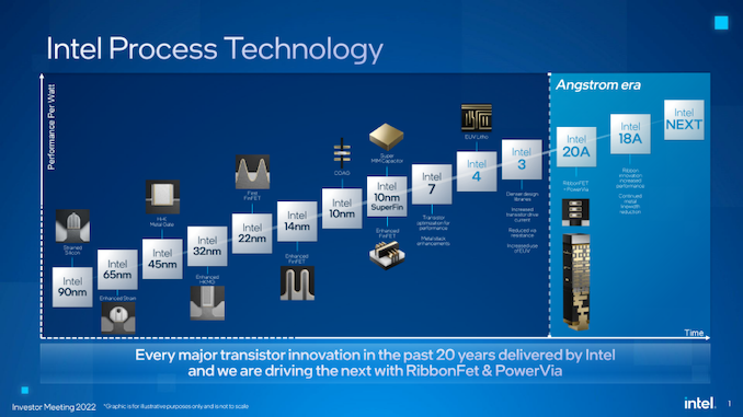
But without Tower Semiconductor, its customer base, and experienced management, the mid-term success of IFS will rely on several pillars: Intel 16 fabrication technology aimed at inexpensive chips, Intel 3 manufacturing process that looks to be optimized primarily for datacenter-bound processors, leading-edge 20A and 18A production nodes that promise to be more innovative than competitors, and Intel’s advanced packaging technologies coupled with vast packaging capacities. Intel’s ability to offer vertically integrated services that include wafer processing and chip packaging will also play an essential role in the success of its IFS division.  


We are building a differentiated customer value proposition as the world’s first open system foundry, with the technology portfolio and manufacturing expertise that includes packaging, chiplet standards and software, going beyond traditional wafer manufacturing,” said Pann.


Source: Intel


Source: AnandTech – Intel Calls Off Tower Acquisition, Forced to Focus Solely on Leading-Edge Nodes

AI Server Market to Reach $150 Billion by 2027 – Foxconn

Demand for generative AI services is skyrocketing and driving the need for AI servers and machines that are substantially different from traditional servers. The category is growing so quickly that sales of AI servers are set to reach $150 billion in 2027, according to Liu Yangwei, the chairman of Foxconn, the world’s largest electronics manufacturing service (EMS) provider.


AI servers are a relatively new category of data center-grade products that use compute GPUs or specialized processors equipped with fast memory, so they tend to be considerably more expensive than traditional servers for data center and enterprise workloads. Demand for various generative AI applications is driving demand for such machines so rapidly that the AI server market will grow from $30 billion in 2023 to a staggering $150 billion by 2027, said Liu Yangwei at the earnings call with analysts and investors this week, reports Commercial Times.


To put the $150 billion number into context, the total server market value reached $123 billion in 2022 and is poised to grow to $186 billion in 2027, according to IDC. If estimates by the Foxconn chairman turn out to be correct, then the market of AI servers will be comparable to the market of traditional servers in four years. This fourfold increase in just four years underscores the explosive demand and the vast opportunities it presents for industry players, including Foxconn.


Foxconn identified cloud service providers (CSPs) as the main clients for AI servers. Cloud giants like Amazon Web Services, Google, and Microsoft Azure continuously seek advanced server solutions to enhance their service offerings and cater to the growing AI needs of their customers. While branded server makers contribute to the demand, CSPs remain the dominant force driving the growth of the AI server market.


The chairman of Foxconn revealed that the company holds over 70% of the market share in the AI server industry’s front-end GPU modules and boards and that it has long-standing relationships with North American CSPs. Since Foxconn has production facilities in the U.S., including the well-known factory in Wisconsin, it can offer localized services to customers like AWS, Google, and Microsoft, a distinct competitive advantage. 


Source: Commercial Times (via Dan Nystedt)


Source: AnandTech – AI Server Market to Reach 0 Billion by 2027 – Foxconn

OWC Teams Up with Frore for 32TB and 64TB SSD Devices

OWC and Frore Systems demonstrated silent 32 TB and 64 TB solid-state storage devices that use Frore’s AirJet Mini coolers at the Flash Memory Summit 2023. Both devices promise consistently high performance while remaining completely quiet. Furthermore, using Frore’s AirJet cooling systems opens doors to high-capacity SSD storage solutions that do not use fans.


OWC demonstrated its 64 TB Mercury Pro U.2 Dual with eight 8 TB M.2-2280 SSDs inside and its 32 TB U2 Shuttle with four 8 TB M.2 drives inside at the show. The peripherals maker said that with the AirJet Mini technology, its 64 TB OWC Mercury Pro U.2 Dual achieves consistent sequential write speeds of 2200 MB/s to 2600 MB/s. However, it does not disclose how fast such a configuration is when only an internal fan is used. OWC says on its website that the enclosure can saturate a Thunderbolt 3 interconnection with up to 2800 MB/s read/write speed when equipped with multiple drives.


OWC’s Mercury Pro U.2 Dual and U2 Shuttle are essentially PCIe 3.0 SSD carriers, and such drives do not tend to get very hot, so applying Frore’s premium AirJet cooling technology to them sounds overkill. But there are two things to note here. First, OWC’s Mercury Pro U.2 Dual comes with a 3,000-rpm fan, and the device is not completely quiet out-of-box, so using AirJets removes the fan and makes it utterly quiet. Secondly, by using Frore’s AirJets with existing carriers, OWC sets the stage for subsequent generations of Mercury Pro U.2 Dual and U2 Shuttle that will house faster and hotter SSDs requiring decent cooling to ensure consistent performance.


Frore’s thin membrane-based AirJet Mini measures 41.5 mm × 27.5 mm × 2.8mm and weighs 11 grams; it is designed to dissipate 5W of heat, and integrating multiple chips amplifies the heat removal capacity proportionally. Modern PCIe Gen5 drives can dissipate considerably more than 5W under high load so they will need more than one AirJet Mini.


It is very exciting to see the application and benefits for our solutions that the Frore Airjet system presents,” said Larry O’Conner, CEO of OWC. “I look forward to taking our solutions further and farther in partnership with Frore. The many ways this technology allows us to increase capacity, long term level up design, improve customer experience and application suitability has opportunities that are endless.


Source: AnandTech – OWC Teams Up with Frore for 32TB and 64TB SSD Devices

Intel and Synopsys Ink Deal to Develop IP for Intel's 3 and 18A Nodes

Intel and Synopsys this week signed an agreement under which Synopsys will develop a portfolio of various IP offerings for Intel 3 and 18A fabrication technologies for Intel Foundry Services (IFS) customers. The availability of industry-standard IP from Synopsys will significantly simplify the development of chips for both current and potential IFS customers. A noteworthy thing about the announcement is that Intel now positions its 3 nm-class node for external clients.


Under this agreement, Synopsys will adapt a variety of its standardized interface IP to Intel’s 3 nm and 1.8 nm-class manufacturing technologies. The availability of standard IP designed specifically for Intel 3 and Intel 18 production nodes will facilitate faster design execution and project timelines for system-on-chips (SoCs). The companies already have an agreement in place under which Synopsys develops electronic design automation (EDA) tools for Intel’s fabrication processes to maximize power, performance, and area scaling for Intel’s upcoming technologies.


The readiness of EDA software and IP is crucial for the adoption of process technology by fabless chip designers, and it is hard to overestimate the importance of the collaboration between Intel and Synopsys. But while the development of IP for the Intel 18A node is something expected, the inclusion of Intel 3 into the deal is a bit surprising since the company has never positioned this manufacturing process for external customers.


The Intel 3 manufacturing technology (previously known as Intel 5 nm) is the company’s 2nd generation node to use extreme ultraviolet lithography. Offering an 18% improvement in performance per watt, a denser library, reduced resistance, and increased drive current, Intel 3 is ideal for data center-grade products. Intel has introduced two data center processors, Granite Rapids and Sierra Forest, using this technology. IFS will build a custom data center product for a cloud service provided with this process. Intel’s client roadmap does not contain any products to use Intel 3, but it looks like it wants to make it available to a broader range of IFS customers.


Marking another important step in our IDM 2.0 strategy, this transaction will foster a vibrant foundry ecosystem by allowing designers to fully realize the advantages of Intel 3 and Intel 18A process technologies and quickly bring differentiated products to market,” said Stuart Pann, senior vice president and general manager of IFS. “Synopsys brings a strong track record of delivering high-quality IP to a broad customer base, and this agreement will help accelerate the availability of IP on advanced IFS nodes for mutual customers.


Source: AnandTech – Intel and Synopsys Ink Deal to Develop IP for Intel’s 3 and 18A Nodes

Samsung, MemVerge, and H3 Build 2TB CXL Memory Pool

Samsung, MemVerge, H3 Platform, and XConn have jointly unveiled their 2 TB Pooled CXL Memory System at the Flash Memory Summit. The device can be connected to up to eight hosts, allowing them to use its memory when needed. The 2 TB Pooled CXL Memory system has software enabling it to visualize, pool, tier, and dynamically allocate memory to connected hosts.


The 2 TB Pooled CXL Memory system is a 2U rack-mountable machine built by H3 with eight 256 GB Samsung CXL memory modules connected using XConn’s XC50256 CXL 2.0 switch supporting 256 PCIe Gen5 lanes and 32 ports. The firmware of the 2 TB Pooled CXL Memory system allows you to connect it to up to eight hosts that can dynamically use CXL memory when they need it, thanks to software by MemVerge.


The Pooled CXL Memory system was developed to overcome limitations in memory capacity and composability in today’s system architecture, which involves tight coupling between CPU and DRAM. Such architecture leads to performance challenges in highly distributed AI/ML applications, such as spilling memory to slow storage, excessive memory copying, I/O to storage, serialization/deserialization, and Out-of-Memory errors that can crash applications.


Attaching 2 TB of fast, low-latency memory using a PCIe 5.0 interface with the CXL 2.0 protocol on top to eight host systems and using it dynamically between eight hosts saves a lot of money while providing loads of performance benefits. According to companies, the initiative represents a significant step towards creating a more robust and flexible memory-centric data infrastructure for modern AI applications.


Modern AI applications require a new memory-centric data infrastructure that can meet the performance and cost requirements of its data pipeline,” said Charles Fan, CEO and co-founder of MemVerge. “Hardware and software vendors in the CXL Community are co-engineering such memory-centric solutions that will deeply impact our future.


The jointly developed demonstration system can be pooled, tiered with main memory, and dynamically provisioned to applications with Memory Machine X software from MemVerge and its elastic memory service. Viewer service showcases the system’s physical layout and provides a heat map indicating memory capacity and bandwidth consumption per application. 


The concept system unveiled at Flash Memory Summit is an example of how we are aggressively expanding its usage in next-generation memory architectures,” said JS Choi, Vice President of New Business Planning Team at Samsung Electronics. “Samsung will continue to collaborate across the industry to develop and standardize CXL memory solutions, while fostering an increasingly solid ecosystem.


Source: AnandTech – Samsung, MemVerge, and H3 Build 2TB CXL Memory Pool

SK Hynix Launches 24GB LPDDR5X-8500 Stacks for Smartphones, PCs, and HPC

On Friday, SK Hynix said it had started mass production of 24 GB LPDDR5X memory stacks that can be used for ultra-high-end smartphones and PCs. The company’s LPDDR5X-8500 devices combine ultra-high-performance with high density, thus enabling fast systems with sufficient memory capacity. SK Hynix says such modules could be used well beyond smartphones, PCs, and even servers.


SK Hynix’s 24 GB LPDDR5X package features an 8500 MT/s data transfer rate and a wide 64-bit interface, thus offering a peak bandwidth of 68 GB/s in the ultra-low voltage range of 1.01 to 1.12V. From a typical PC perspective, this is comparable to bandwidth provided by a dual-channel DDR5-4800 memory subsystem (76.8 GB/s), but at considerably lower power and an orders of magnitude smaller footprint.


An interesting wrinkle of the SK Hynix’s announcement is that the company started to supply these 24 GB LPDDR5X modules well before the announcement as the devices are already used in Oppo’s Oneplus Ace 2 Pro smartphone launched on August 10, 2023.


Oppo is not the only maker of high-end Android smartphones out there, so I would expect more companies to follow suit in the coming months as they roll out handsets based on the Qualcomm Snapdragon 8 Gen 2 system-on-chip.


But SK Hynix envisions its LPDDR5X devices to be used beyond smartphones, so think PCs. Apple was the first company to use LPDDR for desktops and laptops. Still, now that PC SoCs from AMD and Intel support LPDDR5X expect other leading makers of notebooks to adopt LPDDR5X in general and SK Hynix’s 24 GB packages in particular.


Meanwhile, 64-bit LPDDR5X-8500 devices look particularly compelling for the automotive industry, combining performance, capacity, and a very compact form factor. Given the fact that modern infotainment systems require high memory bandwidth, such memory devices will be pretty beneficial. SK Hynix says these memory stacks could be used for servers and even high-performance computing (HPC) applications.


Along with a faster advancement in broader IT industry, our LPDDR products will be able to support a growing list of applications such as PC, server, high-performance computing (HPC) and automotive vehicles,” said Myoungsoo Park, Vice President and Head of DRAM Marketing at SK Hynix. “The company will cement our leadership in the premium memory market by providing the highest performance products that meet customers’ needs.


Source: SK Hynix


Source: AnandTech – SK Hynix Launches 24GB LPDDR5X-8500 Stacks for Smartphones, PCs, and HPC

Samsung Teases 256 TB SSD: 3D QLC NAND at Its Best

Samsung teased the industry’s first 256 TB solid-state drive at the Flash Memory Summit 2023. The new drive features unprecedented storage density and is aimed primarily at hyper-scale data centers where storage density and reduced power consumption matter the most.


Samsung’s 256 TB SSD is based on 3D QLC NAND memory and probably uses innovative packaging to cram multiple 3D QLC NAND devices into stacks. The company does not disclose which form factor the drive uses. Still, because the unit is aimed mainly at hyper scalers, we expect Samsung to offer them in one of the emerging ESDFF form factors or Samsung’s proprietary NGSFF form factor. For now, the only thing that Samsung discloses about its 256 TB SSD is that it is several times more energy efficient than existing drives that carry 32 TB of raw NAND.


Compared to stacking eight 32 TB SSDs, one 256 TB SSD consumes approximately seven times less power, despite storing the same amount of data,” a statement by Samsung reads.


In addition to teasing its 256 TB SSD, Samsung formally announced its next-generation datacenter PM9A3a family of drives with a PCIe 5.0 x4 interface that is expected to offer serious performance and high power efficiency. 


Samsung says that its new PM9A3a SSDs increase sequential read performance by up to 2.3 times (i.e., to 14.95 GB/s) and random write performance by more than 2x compared to the previous generation PM9A3, which uses a PCIe 4.0 x4 interface. In addition, these new drives promise a 60% power efficiency improvement (presumably compared to predecessors) and enhanced Telemetry and Debug functions. 


Samsung’s PM9A3a SSDs will be available in various form factors in the first half of 2024, featuring capacities from 3.84 TB all the way up to 30.72 TB.


Source: Samsung


Source: AnandTech – Samsung Teases 256 TB SSD: 3D QLC NAND at Its Best

Memory Makers on Track to Double HBM Output in 2023

TrendForce projects a remarkable 105% increase in annual bit shipments of high-bandwidth memory (HBM) this year. This boost comes in response to soaring demands from AI and high-performance computing processor developers, notably Nvidia, and cloud service providers (CSPs). To fulfill demand, Micron, Samsung, and SK Hynix are reportedly increasing their HBM capacities, but new production lines will likely start operations only in Q2 2022.


More HBM Is Needed


Memory makers managed to more or less match the supply and demand of HBM in 2022, a rare occurrence in the market of DRAM. However, an unprecedented demand spike for AI servers in 2023 forced developers of appropriate processors (most notably Nvidia) and CSPs to place additional orders for HBM2E and HBM3 memory. This made DRAM makers use all of their available capacity and start placing orders for additional tools to expand their HBM production lines to meet the demand for HBM2E, HBM3, and HBM3E memory in the future.


However, meeting this HBM demand is not something straightforward. In addition to making more DRAM devices in their cleanrooms, DRAM manufacturers need to assemble these memory devices into intricate 8-Hi or 12-Hi stacks, and here they seem to have a bottleneck since they do not have enough TSV production tools, according to TrendForce. To produce enough HBM2, HBM2E, and HBM3 memory, leading DRAM producers have to procure new equipment, which takes 9 to 12 months to be made and installed into their fabs. As a result, a substantial hike in HBM production is anticipated around Q2 2024, the analysts claim.


A noteworthy trend pinpointed by TrendForce analysts is the shifting preference from HBM2e (Used by AMD’s Instinct MI210/MI250/MI250X, Intel’s Sapphire Rapids HBM and Ponte Vecchio, and Nvidia’s H100/H800 cards) to HBM3 (incorporated in Nvidia’s H100 SXM and GH200 supercomputer platform and AMD’s forthcoming Instinct MI300-series APUs and GPUs). TrendForce believes that HBM3 will account for 50% of all HBM memory shipped in 2023, whereas HBM2E will account for 39%. In 2024, HBM3 is poised to account for 60% of all HBM shipments. This growing demand, when combined with its higher price point, promises to boost HBM revenue in the near future.


Just yesterday, Nvidia launched a new version of its GH200 Grace Hopper platform for AI and HPC that uses HBM3E memory instead of HBM3. The new platform consisting of a 72-core Grace CPU and GH100 compute GPU, boasts higher memory bandwidth for the GPU, and it carries 144 GB of HBM3E memory, up from 96 GB of HBM3 in the case of the original GH200. Considering the immense demand for Nvidia’s offerings for AI, Micron — which will be the only supplier of HBM3E in 1H 2024 — stands a high chance to benefit significantly from the freshly released hardware that HBM3E powers.


HBM Is Getting Cheaper, Kind Of


TrendForce also noted a consistent decline in HBM product ASPs each year. To invigorate interest and offset decreasing demand for older HBM models, prices for HBM2e and HBM2 are set to drop in 2023, according to the market tracking firm. With 2024 pricing still undecided, further reductions for HBM2 and HBM2e are expected due to increased HBM production and manufacturers’ growth aspirations.


In contrast, HBM3 prices are predicted to remain stable, perhaps because, at present, it is exclusively available from SK Hynix, and it will take some time for Samsung to catch up. Given its higher price compared to HBM2e and HBM2, HBM3 could push HBM revenue to an impressive $8.9 billion by 2024, marking a 127% YoY increase, according to TrendForce.


SK Hynix Leading the Pack


SK Hynix commanded 50% of the HBM memory market in 2022, followed by Samsung with 40% and Micron with a 10% share. Between 2023 and 2024, Samsung and SK Hynix will continue to dominate the market, holding nearly identical stakes that sum up to about 95%, TrendForce projects. On the other hand, Micron’s market share is expected to hover between 3% and 6%.


Meanwhile, (for now) SK Hynix seems to have an edge over its rivals. SK Hynix is the primary producer of HBM3, the only company to supply memory for Nvidia’s H100 and GH200 products. In comparison, Samsung predominantly manufactures HBM2E, catering to other chip makers and CSPs, and is gearing up to start making HBM3. Micron, which does not have HBM3 in the roadmap,  produces HBM2E (which Intel reportedly uses for its Sapphire Rapids HBM CPU) and is getting ready to ramp up production of HBM3E in 1H 2024, which will give it a significant competitive advantage over its rivals that are expected to start making HBM3E only in 2H 2024.


Source: AnandTech – Memory Makers on Track to Double HBM Output in 2023

Silicon Motion Readies PCIe Gen5 SSDs with 3.5W Power Consumption

Virtually all PCIe Gen5 SSDs released to date are relatively power-hungry and require a massive cooling system, effectively preventing their installation into compact desktops and notebooks. But Silicon Motion’s next-generation SM2508 SSD platform promises to change that and enable ultra-high-performance drives with a PCIe 5.0 interface and power consumption as low as 3.5W. The company is showcasing prototypes of its PCIe Gen5 client drives at the Flash Memory Summit 2023.


The Silicon Motion SM2508 SSD controller features eight NAND channels supporting interface speed of up to 3600 MT/s per channel and capable of delivering sequential read and write speeds of up to 14 GB/s as well random read and write speeds of up to 2.5 million IOPS, which is comparable to capabilities of enterprise-grade SSDs with a PCIe 5.0 x4 interface. 


Perhaps the most critical aspect of the SM2508 is its reduced power consumption, which is around 3.5W, according to Silicon Motion. SMI does not disclose whether 3.5W is idle, average, or peak power consumption, but 3.5W seems to be too high for peak, and even if it is average power consumption, it is considerably lower when compared to the average power consumption of PCIe Gen5 SSDs based on the Phison PS5026-E26 controller (around 10W).


The fastest 3D NAND flash memory devices currently feature a 2400 MT/s interface. Using such memory is crucial to fully saturate a PCIe 5.0 x4 interface and deliver sequential read/write performance of 13 – 14 GB/s. Support for a 3600 MT/s ONFI/Toggle DDR interface will allow the building of ultra-fast SSDs without using many memory devices, which is essential as next-generation 3D TLC devices are expected to have capacities of 1 Tb and larger.


Silicon Motion does not disclose many details about its SM2508, but we know from unofficial sources that the chip is made on TSCM’s 12FFC (12 nm-class, compact low-power production node) and has been sampling since January 2023. Meanwhile, the company has targeted late 2023 – early 2024 as the launch timeframe for its consumer PCIe Gen5 SSD platform.


In addition to demonstrating its first client PC-bound SM2508-based SSDs at the FMS 2023, Silicon Motion is showcasing its MonTitan turnkey enterprise PCIe Gen5 x5 SSD solutions based on its SM8366 controller introduced last year. The SM8366 controller features 16 NAND channels at 2400 MT/s and can enable SSDs with capacities of up to 128 TB that offer up to 14 GB/s sequential read/write performance and up to 3M/2.8M random read/write performance. Samples of MonTitan SSDs will be demonstrated at the FMS 2023.


Source: Silicon Motion


Source: AnandTech – Silicon Motion Readies PCIe Gen5 SSDs with 3.5W Power Consumption

SK Hynix Shows Off 321-Layer 3D TLC NAND Device

SK Hynix showcased its 321-layer TLC NAND memory at the Flash Memory Summit 2023. The South Korean company is the first NAND maker to publicly demonstrate 3D NAND with over 300 layers. Although such memory is expected in mass production in 2025, the demonstration is meant to showcase SK Hynix’s preparedness for the next wave of non-volatile memory technology.


This showcased 321-layer 3D NAND memory device boasts a 1 Tb (128 GB) capacity with TLC architecture, but SK Hynix refrained from revealing other details about it, such as interface speed. Meanwhile, the company mentioned that the chip features a 59% improvement in productivity compared to a 512 Gb 238-layer 3D TLC device, highlighting a significant improvement in per-wafer storage density. Whether or not the new production technology significantly reduces the cost-per-bit of 3D NAND is unclear.


SK Hynix using a 1 Tb 3D TLC device to demonstrate the prowess of its 321-layer 3D NAND process technology may be a good sign, and the company intends to build high-capacity 3D devices on this node. The potential means reduced cost-per-bit compared to existing process nodes. This sets the stage for higher-capacity SSDs and other 3D NAND flash-bases storage devices.


While SK Hynix has yet to reveal the specifics of building 321 active layers, it is safe to assume that the manufacturer used string stacking technology, just like the industry uses it for 200+ layer 3D NAND. However, it is unclear whether SK Hynix stacked two ~160-layer stacks on top of each other or managed to put three ~100+ stacks together.


SK Hynix’s 321-layer 3D TLC NAND device continues to use the company’s CMOS-under-array architecture that puts NAND logic below memory cells to save die space, which is why SK Hynix refers to it as 4D NAND, which is essentially a marketing term.


With another breakthrough to address stacking limitations, SK Hynix will open the era of NAND with more than 300 layers and lead the market,” said Jungdal Choi, head of NAND development at SK Hynix, during a keynote speech. “With timely introduction of the high-performance and high-capacity NAND, we will strive to meet the requirements of the AI era and continue to lead innovation.


Source: SK Hynix


Source: AnandTech – SK Hynix Shows Off 321-Layer 3D TLC NAND Device

Micron's CZ120 CXL Memory Expansion Modules Unveiled: 128GB and 256GB

This week, Micron announced the sample availability of its first CXL 2.0 memory expansion modules for servers that promise easy and cheap DRAM subsystem expansions. 


Modern server platforms from AMD and Intel boast formidable 12- and 8-channel DDR5 memory subsystems offering bandwidth of up to 460.8 – 370.2 GB/s and capacities of up to 6 – 4 TB per socket. But some applications consume all DRAM they can get and demand more. To satisfy the needs of such applications, Micron has developed its CZ120 CXL 2.0 memory expansion modules that carry 128 GB and 256 GB of DRAM and connect to a CPU using a PCIe 5.0 x8 interface.


Micron is advancing the adoption of CXL memory with this CZ120 sampling milestone to key customers,” said Siva Makineni, vice president of the Micron Advanced Memory Systems Group.


Micron’s CZ120 memory expansion modules use Microchip’s SMC 2000-series smart memory controller that supports two 64-bit DDR4/DDR5 channels as well as Micron’s DRAM chips made on the company’s 1α (1-alpha) memory production node. Every CZ120 module delivers bandwidth up to 36 GB/s (measured by running an MLC workload with a 2:1 read/write ratio on a single module), putting it only slightly behind a DDR5-4800 RDIMM (38.4 GB/s) but orders of magnitude ahead of a NAND-based storage device.


Micron asserts that adding four of its 256 GB CZ120 CXL 2.0 Type 3 expansion modules to a server running 12 64GB DDR5 RDIMMs can increase memory bandwidth by 24%, which is significant. Perhaps more significant is that adding an extra 1 TB of memory enables such a server to handle nearly double the number of database queries daily.


Of course, such an expansion means using PCIe lanes and thus reducing the number of SSDs that can be installed into such a machine. But the reward seems quite noticeable, especially if Micron’s CZ120 memory expansion modules are cheaper than actual RDIMMs or have comparable costs.


For now, Micron has announced sample availability, and it is unclear when the company will start to ship its CZ120 memory expansion modules commercially. Micron claims that it has already tested its modules with major server platform developers, so right now, its customers are probably validating and qualifying the modules with their machines and workloads, so it is reasonable to expect CZ120 to be deployed already in 2024.


We have been developing and testing our CZ120 memory expansion modules utilizing both Intel and AMD platforms capable of supporting the CXL standard,” added Makineni. “Our product innovation coupled with our collaborative efforts with the CXL ecosystem will enable faster acceptance of this new standard, as we work collectively to meet the ever-growing demands of data centers and their memory-intensive workloads.


Source: AnandTech – Micron’s CZ120 CXL Memory Expansion Modules Unveiled: 128GB and 256GB

NVIDIA Completes ProViz Ada Lovelace Lineup with Three New Graphics Cards

When NVIDIA began to roll out their Ada Lovelace architecture to the workstation market, the company introduced its new flagship RTX 6000 Ada graphics card meant to offer the highest performance possible as well as its quite spectacular RTX 4000 SFF board that delivers formidable performance in a tiny package. The gap between the two solutions is vast, and on Tuesday, the company finally unveiled new products that fill it.


NVIDIA’s Ada Lovelace-based RTX-series professional graphics cards — the workstation-oriented RTX 4000 20GB, RTX 4500 24GB, RTX 5000 32GB, and the datacenter-bound L40S — graphics are designed for demanding graphics and artificial intelligence workloads, such as computer-aided design, digital content creation, real-time rendering, and basic simulations that are fine with FP32 precision. The new graphics solutions complement NVIDIA’s Ada Lovelace-based workstation boards that have been announced: the midrange RTX 4000 SFF and the ultra-high-end RTX 6000 Ada. Meanwhile, NVIDIA’s previous-generation offerings will continue to serve entry-level workstations based on its Ampere and Turing architectures.


Now, let us cover the new graphics boards in more detail.


NVIDIA’s RTX 4000 20GB is powered by the AD104 graphics processor with 6,144 CUDA cores that promises a peak performance of 26.7 FP32 TFLOPS, which is considerably higher than 19.2 FP32 TFLOPS delivered by the RTX 4000 SFF that features the same GPU with the same configuration albeit working at lower clocks and therefore consuming up to 130W. Unlike the small form-factor board, this uses a full-height PCB but a single-slot cooling system. The novelty is slated for a September release with an MSRP of $1,250.


The more powerful Ada Lovelace-based workstation board is called the RTX 4500, and it uses the AD104 GPU with 7,680 CUDA cores to deliver a compute performance of up to 39.6 FP32 TFLOPS at up to 210W. The board employs a dual-slot cooling system and will be available for $2,250 sometime in October.


Finally, NVIDIA is introducing its RTX 5000 professional graphics card that utilizes the AD102 graphics processor with 12,800 CUDA cores (i.e., a very significant cut down) to achieve a compute performance of 65.3 FP32 TFLOPS at 250W. This board is set to hit the market now for $4,000, which is significantly lower compared to $6,800 for NVIDIA’s flagship RTX 6000 Ada product.


NVIDIA Ada Lovelace Professional Graphics Cards
  RTX 4000 SFF RTX 4000 RTX 4500 RTX 5000 RTX 6000 L40S Ada
GPU AD104 AD104 AD104 AD102 AD102 AD102
CUDA Cores 6,144 6,144 7,680 1,2800 1,8176 1,8176
Memory 20 GB 24 GB 32 GB 48 GB
Power 70W 130W 210W 250W 300W ?
Cooling dual-slot, blower single-slot, blower dual-slot, blower passive
MSRP $1,250 $1,250 $2,250 $4,000 $6,800 ?


NVIDIA’s latest ProViz graphics boards are set to be integrated into the upcoming workstation lineups of renowned companies, including Boxx, Dell, HP, Lambda, and Lenovo. Additionally, the graphics cards will be available for purchase from select graphics card makers like Leadtek, PNY, and Ryoyo, as well as major resellers like Arrow and Ingram. Meanwhile, there will be an Ada Lovelace professional graphics board that will unlikely be available separately.


Catering to the needs of professionals using remote workstations, NVIDIA is launching the L40S Ada datacenter card. The board carries the AD102 graphics processor with 18,176 active CUDA cores, delivering a staggering 91.6 FP32 TFLOPS performance. The product is initially set for NVIDIA’s OVX servers that can be used to enable cloud AI and virtual desktop infrastructure. Still, it is reasonable to expect other AI and VDI infrastructure makers to adopt the L40S Ada board. Interestingly, despite being a data center-oriented product with passive cooling, the L40S Ada includes display outputs, making it suitable for workstations given adequate airflow inside or an attached blower. NVIDIA does not publish the pricing of its OVX machine or the L40S Ada card.


“OVX systems with NVIDIA L40S GPUs accelerate AI, graphics, and video processing workloads and meet the demanding performance requirements of an ever-increasing set of complex and diverse applications,” said Bob Pette, vice president of professional visualization at NVIDIA


Source: AnandTech – NVIDIA Completes ProViz Ada Lovelace Lineup with Three New Graphics Cards

NVIDIA Unveils GH200 'Grace Hopper' GPU with HBM3e Memory

At SIGGRAPH in Los Angeles, NVIDIA unveiled a new variant of their GH200′ superchip,’ which is set to be the world’s first GPU chip to be equipped with HBM3e memory. Designed to crunch the world’s most complex generative AI workloads, the NVIDIA GH200 platform is designed to push the envelope of accelerated computing. Pooling their strengths in both the GPU space and growing efforts in the CPU space, NVIDIA is looking to deliver a semi-integrated design to conquer the highly competitive and complicated high-performance computing (HPC) market.


Although we’ve covered some of the finer details of NVIDIA’s Grace Hopper-related announcements, including their disclosure that GH200 has entered into full production, NVIDIA’s latest announcement is a new GH200 variant with HBM3e memory is coming later, in Q2 of 2024, to be exact. This is in addition to the GH200 with HBM3 already announced and due to land later this year. This means NVIDIA has two versions of the same product, with GH200 incorporating HBM3 incoming and GH200 with HBM3e set to come later.


During their keynote at SIGGRAPH 2023, President and CEO of NVIDIA, Jensen Huang, said, “To meet surging demand for generative AI, data centers require accelerated computing platforms with specialized needs.” Jensen also went on to say, “The new GH200 Grace Hopper Superchip platform delivers this with exceptional memory technology and bandwidth to improve throughput, the ability to connect GPUs to aggregate performance without compromise, and a server design that can be easily deployed across the entire data center.” 


NVIDIA’s GH200 GPU is set to be the world’s first chip, complete with HBM3e memory. In a dual configuration setup, it will be available with up to 282 GB of HBM3e memory, which NVIDIA states “delivers up to 3.5 x more memory capacity and 3 x more bandwidth than the current generation offering.”


Perhaps one of the most notable details NVIDIA shares is that the incoming GH200 GPU with HBM3e is ‘fully’ compatible with the already announced NVIDIA MGX server specification, unveiled at Computex. This allows system manufacturers to have over 100 different variations of servers that can be deployed and is designed to offer a quick and cost-effective upgrade method.


NVIDIA claims that the GH200 GPU with HBM3e provides up to 50% faster memory performance than the current HBM3 memory and delivers up to 10 TB/s of bandwidth, with up to 5 TB/s per chip.


We’ve already covered the announced DGX GH200 AI Supercomputer built around NVIDIA’s Grace Hopper platform. The DGX GH200 is a 24-rack cluster fully built on NVIDIA’s architecture, with each a single DGX GH200 combining 256 chips and offering 120 TB of CPU-attached memory. These are connected using NVIDIA’s NVLink, which has up to 96 local L1 switches providing immediate and instantaneous communications between GH200 blades. NVIDIA’s NVLink allows the deployments to work together with a high-speed and coherent interconnect, giving the GH200 full access to CPU memory and allowing access for up to 1.2 TB of memory when in a dual configuration.


NVIDIA states that leading system manufacturers are expected to deliver GH200-based systems with HBM3e memory sometime in Q2 of 2024. It should also be noted that GH200 with HBM3 memory is currently in full production and is set to be launched by the end of this year. We expect to hear more about GH200 with HBM3e memory from NVIDIA in the coming months


Source: NVIDIA


Source: AnandTech – NVIDIA Unveils GH200 ‘Grace Hopper’ GPU with HBM3e Memory

TSMC Establishes Joint Venture to Build 12nm/16nm Fab in Europe

TSMC on Tuesday announced plans to establish a European Semiconductor Manufacturing Company (ESMC) joint venture with its partners Bosch, Infineon, and NXP to build a fab near Dresden, Germany. The new 300-mm fab will produce chips on TSMC’s 28/22 nm and 16/12 nm-class process technologies, primarily for automotive and industrial sectors. As the project is planned under the European Chips Act framework, TSMC is set to get subsidies to build it.


The proposed ESMC fab will be located near Dresden, Germany, and is slated to have a monthly production capacity of 40,000 300mm wafer starts per month. The fab is set to use TSMC’s 28 nm family of production nodes, which includes several specialty manufacturing technologies and a 22 nm low-power fabrication process with planar transistors and 16 nm and 12 nm production technologies featuring FinFETs. The fab, which TSMC will operate, will employ about 2,000 workers and engineers.


ESMC intends to start fab construction in the latter half of 2024 and start making its first products there by the end of 2027. As TSMC planned, the proposed fab will mainly serve automakers based in Germany and Austria, ensuring a steady supply of chips to these companies in the latter half of the decade. 


This investment in Dresden demonstrates TSMC’s commitment to serving our customer’s strategic capacity and technology needs, and we are excited at this opportunity to deepen our long-standing partnership with Bosch, Infineon, and NXP,” said Dr. CC Wei, Chief Executive Officer of TSMC.


Meanwhile, since the fab will only make chips on mature 12/16 nm and 22/28 nm process technologies, automakers will still need to source advanced processors required for self-driving and sophisticated infotainment systems from TSMC’s fabs in Taiwan and the U.S. Therefore, companies like Bosch, BMW, Infineon, Mercedes Benz Group, NXP, Stellantis, and Volkswagen Group will be able to get various microcontrollers and sensors from ESMC, their most advanced proprietary components that will define capabilities of their software-defined vehicles will be built in Taiwan or the USA. 


Yet, mature process technologies are required not only for automotive and industrial sectors, but also for various emerging applications that fall under the Internet-of-Things umbrella. These will benefit significantly from TSMC’s low-power 22 nm production node and N12e process technology.


Infineon will use the new capacity to serve the growing demand particularly of its European customers, especially in automotive and IoT,” said Jochen Hanebeck, CEO of Infineon Technologies. “The advanced capabilities will provide a basis for developing innovative technologies, products and solutions to address the global challenges of decarbonization and digitalisation.


Financially, the venture is structured such that TSMC will have a 70% stake, with the remaining partners each holding a 10% equity stake. The collective investments for this initiative are forecasted to surpass €10 billion. ESMC is expected to get around €5 billion in subsidies under the Europen Chips Act and from the German government. 


Source: TSMC


Source: AnandTech – TSMC Establishes Joint Venture to Build 12nm/16nm Fab in Europe

Colorful Reveals Mini-ITX GeForce RTX 4060 Ti

Colorful has quietly introduced GeForce RTX 4060 Ti graphics cards in Mini-ITX form-factor that combine compact dimensions and performance of Nvidia’s latest Ada Lovelace GPUs. In fact, with the boosted performance of 22 FP32 TFLOPS, Colorful’s iGame GeForce RTX 4060 Ti Mini OC is likely the highest-performing Mini-ITX graphics card that has been launched to date.


Looking at the options, Colorful has two iGame GeForce RTX 4060 Ti Mini graphics cards in Mini-ITX form-factor: one with 8 GB of GDDR6 memory and another with 16 GB of GDDR6 SGRAM. Both boards are naturally based on Nvidia’s AD106 GPU with 4352 CUDA cores running at 2310 MHz – 2580 MHz, which is slightly higher than Nvidia’s recommended 2540 MHz. The board has four display outputs (four DisplayPort, one HDMI), like fully-fledged GeForce RTX 4060 Ti boards.


Since the boards have a relatively simplistic 6+2-phase voltage regulating module (VRM), it is unlikely that the cards were designed with overclocking in mind, so it is doubtful that these devices can be overclocked significantly. Furthermore, they are equipped with a dual-slot single-fan cooling system with four heat pipes, good enough to dissipate 160W ~ 165W of heat generated by Colorful’s iGame GeForce RTX 4060 Ti Mini. Still, I doubt this cooler will enable great overclocking potential.


Colorful’s iGame GeForce RTX 4060 Ti Mini graphics cards are said to be 199.5 mm long, which is somewhat longer than typical Mini-ITX motherboards, so owners will probably have to ensure compatibility of these AIBs with the chassis.


Compact Mini-ITX PCs are rather popular among gamers these days, but due to the high power consumption of Nvidia’s previous-generation graphics processors did not allow makers of add-in-boards to make Mini-ITX versions of their midrange products. With Ada Lovelace, Nvidia opted to reduce the power consumption of its GeForce RTX 4060-series, which enabled makers of AIBs to experiment with form factors and come up with Mini-ITX versions of GeForce RTX 4060 Ti.


Unfortunately, Colorful’s graphics cards are rare guests in North American and European retailers, so those interested in the company’s iGame GeForce RTX 4060 Ti Mini graphics cards should probably buy directly or from retailers like JD.com.


Given that Nvidia’s GeForce RTX 4060 Ti GPU is readily available from the green company, other makers of graphics cards may follow Colorful with their Mini-ITX versions at some point.


Source: AnandTech – Colorful Reveals Mini-ITX GeForce RTX 4060 Ti

The Be Quiet! Pure Rock 2 FX CPU Cooler Review: For Quiet Contemplation

Today we are taking a look at the Pure Rock 2 FX CPU cooler from the aptly-named and acoustics-focused Be Quiet! One of the company’s latest CPU air coolers, the Pure Rock 2 FX is intended to compete in the packed mainstream cooler market as a competitively priced all-rounder. Always a careful balancing act for cooler vendors, the mainstream market lives up to its name by being where the bulk of sales are, but it’s also the most competitive segment of the market, with numerous competing vendors all chasing the same market with their own idea of what a well-balanced cooler should be. So a successful cooler needs to stand out from the crowd in some fashion – something that’s no easy task when all of them are beholden to the same laws of physics.

So does Be Quiet’s latest cooler have that exceptional factor to make it memorable? We will see where the Pure Rock 2 FX stands in this review.


Source: AnandTech – The Be Quiet! Pure Rock 2 FX CPU Cooler Review: For Quiet Contemplation

Kioxia's CD8P SSD Unveiled: Up to 30.72 TB, PCI 5.0 x4 Interface

Hyperscale data centers have very specific requirements for different tiers of storage devices: some tiers need maximum performance, and others demand maximum storage density. Kioxia’s new CD8P drives for data centers seem to combine both high storage capacity of up to 30.72 TB and high sequential read performance of up to 12,000 MB/s and up to 2 million random read IOPS, which somewhat blurs the lines between storage tiers and provides new opportunities.


Kioxia’s CD8P single-port drives are based on the company’s proprietary controller, firmware, and time-proven 112-layer BICS 5 3D TLC NAND memory. The NVMe 2.0-compliant controller and firmware fully support enterprise-grade features like the company’s exclusive flash die failure protection, power loss protection, end-to-end data protection, sanitize instant erase (SIE), and self-encrypting drive (SED). Since the new SSDs are designed for hyperscale data centers, they come in E3.S and U.2 form factors.


Regarding performance, Kioxia’s new CD8P SSDs offer up to 12,000/5,500 MB/s sequential/write speed and up to 2,000,000/400,000 random read/write 4K IOPS. Meanwhile, there will be two versions of CD8P: CD8P-V for mixed-use applications with up to three drive writes per day with capacities up to 12.8 TB and CD8P-R for read-intensive workloads with up to one drive writes per day capacities of 30.72 TB.


An avid reader will undoubtedly notice that the CD8P family of SSDs is not Kioxia’s first lineup of high-capacity drives with a PCIe Gen5 x4 interface, as the company has been shipping its CM7-series SSDs for about a year now. This is, of course, correct, but Kioxia’s CM7 is designed for enterprise environments, which is why they support dual-port for extended availability, FIPS SED capability, and maximized performance (up to 14 GB/s and 2.7 million 4K IOPS). Hyperscalers barely need such functionality, and the lack of it will probably make CD8Ps slightly cheaper than CM7 drives.


Kioxia positions its CD-series SSDs for s broad range of scale-out and cloud workloads, and indeed, these applications will benefit from their extended performance and capacity. In addition, these new drives could be used for various AI-oriented workloads (particularly on the edge) that can take advantage of high storage density, high performance, and prices that promise to be below those of enterprise-oriented CM7.


Kioxia has not decided when it plans to start shipping its CD8P SSD lineup of SSDs. Still, since hyper scalers need some time to validate and qualify the new storage devices, these new drives will take some time to leave assembly factories. Meanwhile, companies that will use CD8P drives for things like edge AI deployments may deploy these new SSDs somewhat faster if they find them suitable for their workloads.


Source: AnandTech – Kioxia’s CD8P SSD Unveiled: Up to 30.72 TB, PCI 5.0 x4 Interface

Gigabyte Launches Low-Profile GeForce RTX 4060 Graphics Card

The relatively low power consumption of Nvidia’s GeForce RTX 4060 graphics processor allows graphics card makers to experiment with the form factors of their products. We have already seen Mini-ITX GeForce RTX 4060 graphics cards, and late last week, Gigabyte introduced a low-profile GeForce RTX 4060 that can fit into miniature desktops and provide decent performance in games.


The Gigabyte GeForce RTX 4060 OC Low Profile 8G is based on NVIDIA’s AD107 GPU with 3072 CUDA cores that are paired with 8 GB of 17 GT/s GDDR6 memory using a 128-but interface. To justify the OC (overclocked) moniker in the product name, Gigabyte even clocked the graphics processor at 2475 MHz, which is 15 MHz higher than Nvidia’s recommendations for the RTX 4060 model.


Using a graphics board that requires an eight-pin auxiliary PCIe power connector, it is equipped with a dual-slot triple-fan cooling system featuring dozens of thin aluminum. We can only guess whether the cooler is quiet and whether it is good enough to enable further overclocking, but at least Gigabyte guarantees a GPU boost clock of up to 2475 MHz.


Touching more on the cooler, it is longer than the printed circuit board itself, making the graphics card 182 mm long, so owners of compact systems should measure their chassis to ensure compatibility. Most low-profile PC cases are pretty long, but there are also tiny chassis that may be too small for this card.


Despite being low profile, Gigabyte’s GV-N4060OC-8GL has four display outputs: two DisplayPort 1.4a (up to 4Kp120 or up to 5Kp60) and two HDMI 2.1a (up to 5Kp60 or up to 8Kp60 with DSC), so it can be used for rather serious PCs with up to four monitors.


Gigabyte has not disclosed the recommended pricing of their GeForce RTX 4060 OC Low Profile 8G graphics card. Considering that prices of most GeForce RTX products are hovering around recommended $299 price point, it is unlikely that Gigabyte will attempt to charge a huge premium for the unique form factor of its low-profile GeForce RTX 4060. Still, the compact dimensions are undoubtedly a significant differentiator of this product, and GIGABYTE will likely try to earn something extra from it.


Source: Gigabyte


Source: AnandTech – Gigabyte Launches Low-Profile GeForce RTX 4060 Graphics Card