Samsung T9 Portable SSD Review: A 20 Gbps PSSD for Prosumer Workloads

Samsung’s portable SSD lineup has enjoyed significant market success since the launch of the T1 back in 2015. Despite the release of the Thunderbolt-capable X5 PSSD in 2018, the company has been focusing on the mainstream market. Multiple T series drives have made it to the market over the last 8 years. The product line made the transition to NVMe and USB 3.2 Gen 2 only in 2020 with the launch of the T7 Touch. Today, the company unveiled its first USB 3.2 Gen 2×2 (20 Gbps) PSSD – the Samsung T9. Read on for an in-depth investigation into the design and performance profile of the T9’s 4 TB version.


Source: AnandTech – Samsung T9 Portable SSD Review: A 20 Gbps PSSD for Prosumer Workloads

Asus Formally Completes Acquisition of Intel's NUC Business

ASUS has formally acquired Intel’s Next Unit of Computing (NUC) products based on Intel’s 10th to 13th Generation Core processors. Asus is set to continue building and supporting Intel’s existing NUCs and will, over time, roll out its own compact NUC systems for office, entertainment, gaming, and many other applications.


I am confident that this collaboration will enhance and accelerate our vision for the mini PC,” said Jackie Hsu, Asus senior vice president and co-head of OP & AIoT business groups, at the signing ceremony. “Adding the Intel NUC product line to our portfolio will extend ASUS’s AI and IoT R&D capabilities and technology solutions, especially in three key markets – industrial, commercial, and prosumer.


Asus held a formal handover ceremony in Taipei and took control of the NUC product lines that span from business applications to gaming. With the acquisition, Asus instantly commenced business processes for the NUC range, ensuring a hassle-free transition for existing customers. Under the terms of the agreement, Asus obtained licenses for both Intel’s hardware designs and software. This move widens Asus’s operational scope in R&D and extends its reach in logistics, tech support, and numerous application areas. 


Asus envisions broadening its NUC product line and distribution channels. The focus will remain on offering high-quality compact PCs with robust security and advanced technologies, which NUC is known for. ASUS also aims to produce eco-friendly NUC products while emphasizing impeccable service for its customer base.


This is an exciting time for both Intel and Asus as we move forward with the next chapter in NUC’s story,” said Michelle Johnston Holthaus, Executive Vice President and General Manager of the Client Computing Group at Intel, who also attended the event. “Today’s signing ceremony signifies more than just a business deal. It signifies ASUS’ dedication to enhancing the lives of NUC customers and partners around the world. I look forward to seeing NUC thrive as part of the ASUS family.


It should be noted that Asus’s Intel NUC license is not exclusive, so Intel may eventually enable other PC makers to build its NUCs and, therefore, compete against Apple.


Source: Asus


Source: AnandTech – Asus Formally Completes Acquisition of Intel’s NUC Business

Micron to Ship HBM3E Memory to NVIDIA in Early 2024

Micron has reaffirmed plans to start shipments of its HBM3E memory in high volume in early 2024, while also revealing that NVIDIA is one of its primary customers for the new RAM. Meanwhile, the company stressed that its new product has been received with great interest by the industry at large, hinting that NVIDIA will likely not be the only customer to end up using Micron’s HBM3E.


“The introduction of our HBM3E product offering has been met with strong customer interest and enthusiasm,” said Sanjay Mehrotra, president and chief executive of Micron, at the company’s earnings call.


Introducing HBM3E, which the company also calls HBM3 Gen2, ahead of its rivals Samsung and SK Hynix is a big deal for Micron, which is an underdog on the HBM market with a 10% market share. The company obviously pins a lot of hopes on its HBM3E since this will likely enable it to offer a premium product (to drive up its revenue and margins) ahead of its rivals (to win market share).


Typically, memory makers tend not to reveal names of their customers, but this time around Micron emphasized that its HBM3E is a part of its customer’s roadmap, and specifically mentioned NVIDIA as its ally. Meanwhile, the only HBM3E-supporting product that NVIDIA has announced so far is its Grace Hopper GH200 compute platform, which features an H100 compute GPU and a Grace CPU.


“We have been working closely with our customers throughout the development process and are becoming a closely integrated partner in their AI roadmaps,” said Mehrotra. “Micron HBM3E is currently in qualification for NVIDIA compute products, which will drive HBM3E-powered AI solutions.”


Micron’s 24 GB HBM3E modules are based on eight stacked 24Gbit memory dies made using the company’s 1β (1-beta) fabrication process. These modules can hit date rates as high as 9.2 GT/second, enabling a peak bandwidth of 1.2 TB/s per stack, which is a 44% increase over the fastest HBM3 modules available. Meanwhile, the company is not going to stop with its 8-Hi 24 Gbit-based HBM3E assemblies. The company has announced plans to launch superior capacity 36 GB 12-Hi HBM3E stacks in 2024 after it initiates mass production of 8-Hi 24GB stacks.


“We expect to begin the production ramp of HBM3E in early calendar 2024 and to achieve meaningful revenues in fiscal 2024,” added chief executive of Micron.


Source: AnandTech – Micron to Ship HBM3E Memory to NVIDIA in Early 2024

Micron Samples 128 GB Modules Based on 32 Gb DDR5 ICs

Micron is sampling 128 GB DDR5 memory modules based on monolithic dies, the company said at its earnings call this week. The modules are based on monolithic 32 Gb DDR5 memory devices that the company announced earlier this summer and which will eventually open doors for 1 TB memory modules for servers.


We expanded our high-capacity D5 DRAM module portfolio with a monolithic die-based 128 GB module, and we have started shipping samples to customers to help support their AI application needs,” said Sanjay Mehrotra, president and chief executive of Micron. “We expect revenue from this product in Q2 of calendar 2024.”


Micron’s monolithic 32 Gb DDR5 dies are made on the company’s 1β (1-beta) manufacturing process, which is the last production node that solely relies on multi-patterning using deep ultraviolet (DUV) lithography and does not use extreme ultraviolet (EUV) lithography tools. This is all that we know about Micron’s 32 Gb DDR5 ICs at this point, though: the company does not disclose its maximum speed bin, though we can expect a drop in power consumption compared to two 16 Gb DDR5 ICs operating at the same voltage and data transfer rate.


Micron’s new 32 Gb memory chips pave the way for creating a standard 32 GB module for personal computers with just eight individual memory chips and a server-oriented 128 GB module based on 32 of such ICs. Moreover, these chips make producing memory modules with a 1 TB capacity feasible, deemed unattainable today. These 1 TB modules might seem excessive for now, but they benefit fields like artificial intelligence, Big Data, and server databases. Such modules can enable servers to support up to 12 TB of DDR5 memory per socket (in the case of a 12-channel memory subsystem).


Speaking of DDR5 memory in general, it is noteworthy that the company expects that its bit production of DDR5 will exceed that of DDR4 in early 2024, placing it a bit ahead of the industry.


Micron also has a strong position in the industry transition to D5,” said Mehrotra. “We expect Micron D5 volume to cross over D4 in early calendar 2024, ahead of the industry.” 


Source: Micron


Source: AnandTech – Micron Samples 128 GB Modules Based on 32 Gb DDR5 ICs

Intel Meteor Lake SoC is NOT Coming to Desktops: Well, Not Technically

Over the last couple of days, numerous reports have revealed that Intel’s recently announced Meteor Lake SoC, primarily a mobile platform, would be coming to desktop PCs. Intel has further clarified that while their Meteor Lake processors will be featured in desktop systems next year, they won’t power traditional socketed desktop PCs. Instead, these CPUs, primarily crafted for laptops, will be packaged in ball grid array (BGA) formats, making them suitable for compact desktops and all-in-one (AIO) devices.


Intel’s statement, as reported by ComputerBase, emphasizes, “Meteor Lake is a power efficient architecture that will power innovative mobile and desktop designs, including desktop form factors such as All-in-One (AIO). We will have more product details to share in the future.” 


A senior Intel official recently mentioned that Meteor Lake processors are slated for desktop release in 2024. However, they won’t be available in Intel’s LGA1851 form factor, which caters to gaming rigs, client workstations, and conventional desktop systems. The practice of integrating laptop CPUs into compact PCs, such as NUCs and all-in-one PCs, isn’t a novel one. Manufacturers have been doing this for years, and the intriguing aspect will be observing the performance and efficiency metrics of these high-end Meteor Lake laptop CPUs, especially when juxtaposed against the existing Raptor Lake processors designed for both desktops and laptops.


The rationale behind Intel’s decision to exclude Meteor Lake processors from socketed desktops remains ambiguous. The CPU employs a multi-tile structure, with its compute tile being developed on the Intel 4 process technology. This technology marks Intel’s inaugural use of extreme ultraviolet lithography (EUV), while the graphics tile and SoC leverage TSMC’s fabrication methods. Both production techniques are poised to deliver commendable performance and efficiency, but Meteor Lake is not designed as a pure desktop product.


Current indications suggest that the Arrow Lake-S series will be aimed at LGA1851 motherboards, but this is anticipated for the latter half of 2024. While Q3/Q4 of 2024 is still a while away, Intel’s motherboard partners, such as GIGABYTE and MSI, have been readying up new refreshed Z790 motherboards, with features such as Wi-Fi 7 set to come to Intel’s impending Raptor Lake refresh platform which is due sometime before the end of the year.


Source: ComputerBase


Source: AnandTech – Intel Meteor Lake SoC is NOT Coming to Desktops: Well, Not Technically

eMMC Destined Live A Bit Longer: KIOXIA Releases New Generation of eMMC Modules

While the tech industry as a whole is well in the middle of transitioning to UFS and NVMe storage for portable devices, it would seem that the sun won’t be setting on eMMC quite yet. This week Kioxia has introduced a new generation of eMMC 5.1 modules, based around a newer generation of their 3D NAND and aimed at those final, low-budget devices that are still using the older storage technology.


Kioxia’s new storage modules are compliant with the eMMC 5.1 standard, offering sequential read performance that tops out at 250 MB/s – the best that this technology can provide. But the internal upgrade to a newer generation of Kioxia’s 3D NAND can still provide some benefits over older modules, including 2.5x higher sequential and random write performance as well as 2.7x higher random read performance. Also, the new eMMC modules are spec’d to be more durable, with an up to 3.3 higher TBW rating over predecessors.


“e-MMC remains a popular embedded memory solution for a wide range of applications,” said said Maitry Dholakia, vice president, Memory Business Unit, for Kioxia America. “Kioxia remains steadfast in its commitment to delivering the latest in flash technology for these applications. Our new generation brings new performance features which address end user demands – and create a better user experience.”


Given that the remaining devices using eMMC storage fall into the simplistic and inexpensive category, the new lineup of Kioxia’s eMMC modules only includes packages offering 64GB and 128GB of storage. Which, in the big picture, is a small amount of storage – but it’s suitable for budget devices, as well as for electronics with limited storage needs, such as drones, digital signage, smart speakers, and TVs.


But the main idea behind the new eMMC modules from Kioxia is perhaps not to improve their performance and user experience, but rather use newer and cheaper 3D NAND memory with them. This enables Kioxia to address inexpensive applications more cost efficiently, which ensures that the company will continue doing it going forward.


Kioxia expects to start mass production of its new 64 GB and 128 GB eMMC 5.1 storage modules in 2024. The company is sampling the new devices with its partners at present.


Source: AnandTech – eMMC Destined Live A Bit Longer: KIOXIA Releases New Generation of eMMC Modules

Crucial Unveils X9 Portable SSD: QLC for the Cost-Conscious Consumer

Crucial entered the portable SSD market relatively late, with their X6 and X8 PSSDs being the mainstay for many years. Based on QLC NAND, they were marketed for read-intensive use-cases, though the generous amount of SLC cache ended up delivering good write performance too for mainstream consumers – particularly in the X8. Recently, the company also started focusing on the prosumer / power users market with the launch of the X9 Pro and X10 Pro. Based on Micron’s 176L 3D TLC NAND, these drives came with guaranteed write speeds.


Earlier this week, the company launched a successor to the Crucial X8 in the same form-factor as that of the recently launched X9 Pro and X10 Pro. The new USB 3.2 Gen 2 Crucial X9 PSSD takes on the same 65 x 50mm dimensions, but opts for an ABS plastic enclosure instead of the metal one used in the Pro units. Similar to the X8 that is being replaced, the X9 also doesn’t advertise write speeds and there is no hardware encryption available. The lanyard hole is retained from the Pro design, but the LED indicator has been dropped. While the X9 is drop-proof up to 2m, the water- and dust-resistance features are not included.


The Crucial X9 PSSD utilizes Micron’s 176L 3D QLC NAND and retains the Phison U17 native flash controller. The 1TB, 2TB, and 4TB capacity points are being introduced at $80, $120, and $250, though Amazon currently lists them at $90, $140, and $280 respectively. It is no secret that there is a glut in the flash market currently, resulting in very attractive (P)SSD price points for consumers. However, it is also well-known that it is a cyclic trend. Industry observers expect prices to go up sometime next year, and based on inventory levels of various models with different retailers, we might see strange pricing swings.


The Crucial X9 PSSD is a much-needed upgrade to the aging X8, and we are glad that Crucial has decided to release a new model instead of silently updating the NAND in the older version. The new form-factor and design for this product class is also a welcome change. Crucial’s expanded product lineup ensures that it is competitive against established players like Samsung and Western Digital across all high-volume PSSD market segments. The only missing part is a Thunderbolt / USB4 model, and we hope Crucial will address that in the near future.


Source: AnandTech – Crucial Unveils X9 Portable SSD: QLC for the Cost-Conscious Consumer

Corsair's Dominator Titanium Memory Now Available, Unveils Plans for Beyond 8000 MT/s

Corsair has started sales of its Dominator Titanium memory modules that were formally introduced this May. The new modules bring together luxurious look, customizable design, and extreme data transfer rates of up to 8000 MT/s. Speaking of performance, the company implied that it intends to introduce Dominator Titanium with speed bins beyond DDR5-8000 when the right platform arrives.


Corsair’s Dominator Titanium family is based around 16 GB, 24 GB, 32 GB, and 48 GB memory modules that come in kits ranging from 32GB (2 x 16GB) up to 192GB (4x 48GB). As for performance, the lineup listed at the company’s website includes DDR5-6000 CL30, DDR5-6400 CL32, DDR5-6600 CL32, DDR5-7000 CL34, DDR5-7000 CL36, DDR5-7200 CL34, and DDR5-7200 CL36 with voltages of 1.40 V – 1.45V.


Although Corsair claims that Dominator Titanium with data transfer speeds beyond 8000 MT/s are coming, it is necessary to note that they will be supported by next generation platforms from AMD and Intel. For now, the company only offers 500 First Edition Dominator Titanium kits rated for DDR5-8266 mode for its loyal fans.


To address demand from different types of users, Corsair offers Dominator Titanium with XMP 3.0 SPD settings for Intel’s 12th and 13th Generation Core CPUs with black and white heat spreaders as well as with AMD EXPO SPD profiles for AMD’s Ryzen processors with grey finish on heat spreaders.


In terms of design of heat spreaders, Corsair remained true to aesthetics. The modules are equipped with 11 customizable Capellix RGB LEDs, offering users a personalized touch. This can be easily adjusted using Corsair’s proprietary software. For enthusiasts who lean towards a more traditional aesthetic, Corsair provides an alternative design with fins, reminiscent of their classic memory modules.


Speaking of heat spreaders, it is necessary to note that despite the name of the modules, they do not come with titanium radiators and keep using aluminum, which is a good thing since titanium has a rather low thermal conductivity of 11.4 W/mK and will therefore heat up memory chips rather than distribute heat away from them. Traditionally, Corsair’s Dominator memory modules use cherry-picked DRAM chips and the company’s proprietary printed circuit boards enhanced with internal cooling planes and external thermal pads to improve cooling.


Corsair’s Dominator Titanium memory products are now available both directly from the company and from its resellers. The cheapest Dominator Titanium DDR5-6000 CL30 32 GB kit (2 x 16 GB) costs $175, whereas faster and higher-capacity kits are priced higher.


Source: AnandTech – Corsair’s Dominator Titanium Memory Now Available, Unveils Plans for Beyond 8000 MT/s

GlobalFoundries Applies for CHIPS Money to Expand U.S. Fabs

GlobalFoundries has applied for financial support from the U.S. CHIPS and Science Act to expand its American manufacturing sites, the company said this week. The company intends to get federal grants and investment tax credits to upgrade facilities used to build chips for various applications, including automotive, aerospace, defense, and many other industries.


GlobalFoundries’s initiative is in line with the provisions of the U.S. CHIPS and Science Act, which aims to strengthen the nation’s semiconductor production capabilities. The act has set aside a substantial amount, $52.7 billion, to support semiconductor research, production, and workforce development. Additionally, it offers a 25% investment tax incentive for the construction of chip plants, estimated to be worth around $24 billion, Reuters reminded.


This expansion is beneficial for the company and essential for enhancing the U.S.’s economic stability, supply chain robustness, and defense mechanisms, the company said.


As the leading manufacturer of essential semiconductors for the U.S. government, and a vital supplier to the automotive, aerospace and defense, IoT and other markets, GF has submitted our applications to the CHIPS Program Office to participate in the federal grants and investment tax credits enabled by the U.S. CHIPS and Science Act,” said Steven Grasso, senior director of global government affairs at GF. “This federal support is critical for GF to continue growing its U.S. manufacturing footprint, strengthening U.S economic security, supply chain resiliency, and national defense.


GlobalFoundries is not alone in getting money from the CHIPS fund. The U.S. Department of Commerce said over 460 companies would get these semiconductor subsidies in August. The subsidies aim to foster innovation and ensure the U.S. remains at the forefront of semiconductor technology.


Sources: GlobalFoundriesReuters


Source: AnandTech – GlobalFoundries Applies for CHIPS Money to Expand U.S. Fabs

Modular LPDDR Memory Becomes A Reality: Samsung Introduces LPCAMM Memory Modules

Although Low Power DDR(LPDDR) memory has played a pivotal role in reducing PC laptop power usage, the drawback to the mobile-focused memory has always been its tight signaling and power delivery requirements. Designed to be placed close to its host CPU in order to minimize power expenditures and maximize clockspeeds, LPDDR memory is unsuitable for use in traditional DIMMs and SO-DIMMs – instead requiring that it be soldered down on a device in advance. But it looks like the days of soldered-down LPDDR memory are soon at an end, as this evening Samsung is announcing a new standard for removable and modular LPDDR memory: LPCAMM.


Source: AnandTech – Modular LPDDR Memory Becomes A Reality: Samsung Introduces LPCAMM Memory Modules

Solidigm Introduces D7-P5810: 144L SLC NVMe Drive for Write-Intensive Workloads

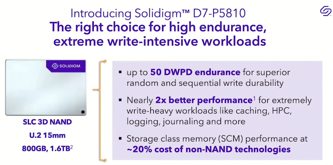
Solidigm’s datacenter SSD offerings have been clearly delineated into different categories – the D3- SATA offerings for legacy servers, the D5- QLC-based offerings (with different models offering different tradeoffs between cost and endurance), and the D7- NVMe drives for the best performance and endurance ratings. The company has been using TLC NAND in the D7 drives so far. Last week, the company introduced a new member in their D7 lineup for extremely write-intensive workloads – the D7-P5810 using their mature 144L SLC 3D NAND.


Storage-class memory (SCM) options such as Optane have been used by hyperscalers for a variety of use-cases such as write-caching, HPC applications, journaling, online transaction processing (OLTP), etc. With the winding down of the Optane product line, many opportunities have opened up for SSD vendors to bring near-SCM type products into the market. We saw Micron introducing their XTR NVMe SSDs earlier this year using their 176L 3D NAND in SLC mode. The company had optimized the firmware on the drives and drawn up specifications for near-Optane performance in Microsoft SQL Server analytics workloads. Solidigm is taking a similar approach with the D7-P5810, albeit with optimizations for a different use-case.


Solidigm took a look at the requirements satisfied by Optane drives in Alibaba’s (Optane + QLC) deployment for local disks in their cloud servers, and figured out that the Optane drives were greatly over-engineered for them. As an example, Alibaba’s workload only demanded 37 DWPD, while Optane provided 100. The 4K random write requirements was also only 8K IOPS per tenant, while Alibaba’s configuration resulted in the Optane drive providing 20K IOPS per tenant. Solidigm has optimized the firmware of the D7-P5810 to meet these requirements by providing 50 DWPD worst-case endurance, and 10K IOPS per tenant at capacities similar to the Optane drives used by Alibaba.


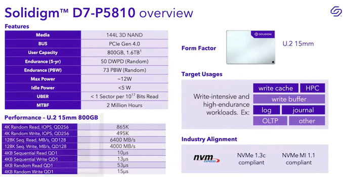
The specifications of the D7-P5810 are summarized below. The 800 GB version of the drive is in mass production, while the 1.6 TB version is expected to make an appearance in the first half of 2024.


The company had a few interesting presentations at Storage Field Day 26, and in one of those, the company put out a slide comparing the D7-P5810 against the competition.


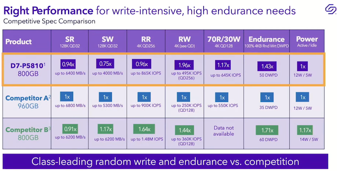
It is not difficult to figure out that Competitor A in the above slide is Micron’s XTR NVMe SSD, while Competitor B is Kioxia’s FL6 Series. Different enterprise SSD use-cases have different requirements in terms of sequential speeds, random access IOPS, endurance, and power consumption. As a result, we are starting to see vendors offer specialized drives with firmware optimized for a particular use-case. The differences in the above comparison can be attributed to the vendor optimizing for different use-cases. Fundamental differences in the flash packages apart (176L in Micron’s XTR vs. 96L BiCS in Kioxia’s FL6 vs. 144L in Solidigm’s D7-P5810), it is likely that these vendors can achieve different tradeoffs with their drive’s firmware if required.


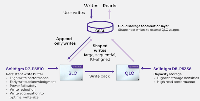
Solidigm acquired Intel’s Cloud Storage Acceleration Layer (CSAL) team earlier this year. At Intel, the group (which had open-sourced its work in the Storage Performance Development Kit) had been working on Optane as an accompanying drive for other slower media. After joining Solidigm, the company has shifted focus from Optane to SLC, with a focus on using drives such as the D7-P5810 as a complement to their high-density QLC drives.


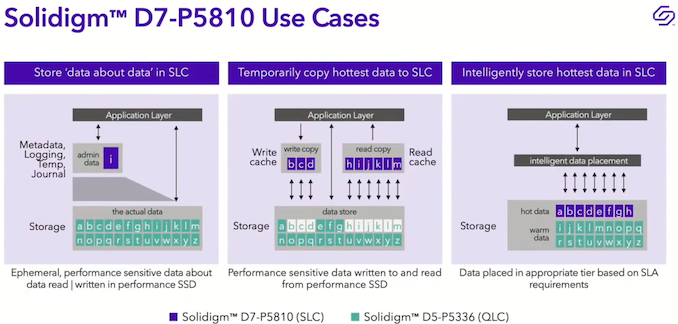
Other than the above use-case in deployment at Alibaba, the D7-P5810 can also be used in a wide variety of scenarios such as metadata storage, caching, and data placement based on service-level agreement (SLA) requirements.


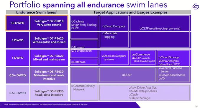
With the inclusion of the D7-P5810, the Solidigm enterprise SSD product line has a product portfolio encompassing a wide range of endurance ratings with suitability for different applications and use-cases.


Optane may be winding down soon, but it is heartening to see vendors like Micron and Solidigm stepping up to provide SLC-based alternatives. By avoiding over-engineering for specific use-cases that are currently being served by Optane drives, the vendors are also able to present enterprise SSD users with a cost-effective solution.


Source: AnandTech – Solidigm Introduces D7-P5810: 144L SLC NVMe Drive for Write-Intensive Workloads

Sabrent Ships 8TB SSD for PlayStation 5: High Capacity for a High Price

Although Sony’s PlayStation 5 game console fully supports off-the-shelf PCIe 4.0 solid-state drives, Sony initially limited the maximum capacity to 4 TB. Recently the company removed that cap as part of the PS5 8.00 firmware update, and now the system can support drives with up to 8 TB. Sabrent, in turn, is among the first SSD makers to offer an 8 TB drive specifically marketed for the PS5.


“PC and PS5 enthusiasts have long anticipated the expansion of internal storage capacity, and now, this dream has become a reality with the introduction of the Sabrent 8TB Rocket 4 Plus SSD,” a statement by Sabrent reads.


Sabrent’s Rocket 4 Plus 8 TB is based on a Phison platform and is actually a bit faster than the rest of the drives in the series. The manufacturer says that the SSD offers an up to 7,100 MB/s sequential write and up to 6,000 MB/s sequential write speeds. In order to keep the drive properly cooled under high loads, the drive comes equipped with a PS5-compatible aluminum heatsink that also doubles as a replacement for the drive bay’s metal cover plate.


Sabrent’s 8 TB Rocket 4 Plus drive (SB-RKT4P-PSHS-8TB) can now be purchased from Amazon for $1,009.99, which is twice the price of Sony’s PlayStation 5 console, and a $10 premium over a bare 8TB Rocket 4 Plus.


This is of course a huge investment, but PS5’s 825 GB of capacity available to end users is a fraction of what modern SSDs can provide 3 years later – and whose small capacity is quickly being consumed by modern, high-end games. For example, Call Of Duty: Black Ops Cold War takes up over 300 GB and Gran Turismo 7 nears 200 GB.


Now that Sony’s PlayStation 5 supports 8 TB SSDs, the console gets a yet another advantage over Microsoft’s Xbox Series X|S consoles, which only support proprietary drives with an up to 2 TB capacity. Since these drives are essentially M.2-2230 SSDs encapsulated into a plastic case, it remains to be seen when an 8 TB drive will come to the latest generation of Xbox consoles.


Source: AnandTech – Sabrent Ships 8TB SSD for PlayStation 5: High Capacity for a High Price

ECS LIVA Q3D and ACEMAGIC T8 Plus micro-PCs Review: Jasper Lake and Alder Lake-N in a Smaller-than-UCFF Package

Compact computing systems have gained significant market share over the last decade. Improvements in the performance per watt metric of processors have enabled the replacement of bulky desktop PCs by ultra-compact form-factor (UCFF) machines with a 4 in. x 4 in. footprint. Motivated by IoT applications at the edge, some companies started creating x86 systems in sub-4×4 form-factors using Intel’s Apollo Lake processors. ECS was one of the first mainstream vendors to pay attention to this segment with their LIVA Q Series using Intel’s Atom series and AMD’s first-generation Ryzen Embedded SoCs. With the introduction of more power-efficient platforms, Asian manufacturers such as ACEMAGIC, GMKtec, and MinisForum have also entered this micro-PC market with a wider range of processor choices.


Intel introduced the Alder Lake-N (ADL-N) product family to take over Jasper Lake’s role in the cost-conscious low-power PC market. As ADL-N ramps up and Jasper Lake winds down, we are seeing products based on both families being actively sold in the market. We took advantage of this opportunity to source two micro-PCs – the LIVA Q3D from ECS, and the T8 Plus from ACEMAGIC – and put them through our evaluation routine to study the benefits of ADL-N’s Gracemont microarchitecture over Jasper Lake’s Tremont. Read on for a detailed look at the results along with a discussion of the tradeoffs involved in pursuing a smaller-than-UCFF footprint.


Source: AnandTech – ECS LIVA Q3D and ACEMAGIC T8 Plus micro-PCs Review: Jasper Lake and Alder Lake-N in a Smaller-than-UCFF Package

Asus Launches ROG Matrix GeForce RTX 4090: All a 4090 Can Be, For $3200

When Asus teased its ROG Matrix GeForce RTX 4090 graphics card back at Computex, it was clear that the company’s ambitions were to develop no less than the world’s fastest graphics card. The company meticulously described the card’s advanced printed circuit board design, voltage regulating module, and cooling system, but it never revealed two important details: actual clocks and price. This week it disclosed both: the board will clock the GPU at 2.70 GHz out-of-box and will cost $3,199, twice the price of a reference GeForce RTX 4090.


An Overclocker’s Dream Comes True


Asus proudly states that the ROG Matrix GeForce RTX 4090 is ideal for overclocking enthusiasts. The board used the AD102 GPU equipped with 16,384 CUDA cores that has a peak frequency of 2700 MHz, surpassing NVIDIA’s reference boost clock of 2520 MHz. In a physically unmodified (but LN cooled) state, an extreme overclocked ROG Matrix GeForce RTX 4090 surpassed the 4 GHz GPU clock threshold earlier this year, an achievement that underscores its potential for overclocking.


Since its debut at Computex, the card has secured three World Records and five top spots, totaling seven overclocking achievements in various benchmarks, Asus says.


NVIDIA has dozens of add-in-board (AIB) partners producing factory overclocked graphics cards. But with EVGA and its Kingpin-edition graphics cards gone, there are not so many brands left which cater to demands of extreme enthusiasts. Asus is certainly one of them and with its range-topping ROG Matrix RTX 4090, the company went above and beyond with enhancements beyond reference designs.


Through Hardware and Software


The card employs a custom circuit board featuring a 24-phase VRM and a 12VHPWR connector, ensuring up to 600W of power for the GPU. This board is equipped with multiple sensors to oversee temperatures of various components (and even create a temperature map) and even measure currents on the card’s 12VHPWR connector (more on this later).


The ROG Matrix GeForce RTX 4090 comes with a comprehensive closed-loop hybrid liquid cooling solution with a 360-mm radiator, magnetically connected fans, and RGB illumination. In a bid to improve efficiency of the cooler, Asus used a liquid metal thermal compound, which it uses for its gaming laptops and which is particularly hard to use for desktop PC components (marking a first in the GPU industry for Asus) since they tend to be located under a different angle.


The ROG Matrix RTX 4090’s strengths are not solely in its hardware though. Asus has enhanced its GPU Tweak III software, adding more monitoring and overclocking capabilities that leverage the card’s advanced features and sensors. Users can customize various settings, including power targets, GPU voltage, and fan speed. The software also offers real-time temperature insights and tracks the card’s performance at varying power settings.


Another notable aspect is the card’s Power Detector+ feature. This function examines the 12VHPWR connector, monitoring currents across all power rails to identify any irregularities, then recommends customers to reconnect the notorious plug if needed.


A Niche Product


Meanwhile, performance of the ROG Matrix RTX 4090 comes at a cost as the product’s price doubles that of a standard GeForce RTX 4090. This greatly devalues the product in the eyes of average people. But the Asus ROG Matrix RTX 4090 is a niche product. It targets hardcore overclocking enthusiasts eager to maximize their hardware’s performance. This card is for those who relish fine-tuning their systems for minor benchmarking improvements, making it a trophy piece for tech enthusiasts.


Source: AnandTech – Asus Launches ROG Matrix GeForce RTX 4090: All a 4090 Can Be, For 00

Intel High-NA Lithography Update: Dev Work On Intel 18A, Production On Future Node

As part of Intel’s suite of hardware announcements at this year’s Intel Innovation 2023 conference, the company offered a brief update on their plans for High-NA EUV machines, which will become a cornerstone of future Intel process nodes. Following some changes in Intel’s process roadmap – in particular Intel 18A being pulled in because it was ahead of schedule – Intel’s plans for the next-generation EUV machines. Intel will now only be using the machines with their 18A node as part of their development and validation work of the new machines; production use of High-NA machines will now come on Intel’s post-18A node.


High Numerical Aperture (High-NA) machines are the next generation of EUV photolithography machines. The massive scanners incorporate 0.55 numerical aperture optics, significantly larger than the 0.33 NA optics used in first-generation production EUV machines, which will ultimately allow for higher/finer quality lines to be etched. Ultimately, High-NA machines are going to be a critical component to enabling nodes below 2nm/20 angstroms.


At the time that Intel laid out their “5 nodes in 4 years” roadmap in 2021, the company announced that they were going to be the lead customer for ASML’s High-NA machines, and would be receiving the first production machine. High-NA, in turn, was slated to be a major part of Intel’s 18A node.


Size Comparison: ASML Normal & High NA EUV Machines


But since 2021, plans have changed for Intel, seeming in a good way. Progress on 18A has been ahead of schedule, such that, in 2022, Intel announced they were pulling in 18A manufacturing from 2025 to H2’2024. Given that the release date of ASML’s High-NA machines has not changed, however, that announcement from Intel left open some questions about how High-NA would fit into their 18A node. And now we finally have some clarification on the matter from Intel.


High-NA machines are no longer a part of Intel’s production plans for 18A. With the node now arriving before production-grade High-NA machines, Intel will be producing 18A with the tools they have, such as ASML’s NXE 3000 series EUV scanners. Instead, the intersection between 18A and High-NA will be that Intel using the 18A line to develop and validate the use of High-NA scanners for future production. After which, Intel will finally use High-NA machines as part of the production process for their next-generation, post-18A node, which is simply being called “Intel Next” right now.


As for the first High-NA development machine, Intel also confirmed this week that their schedule for development remains on track. Intel is slated to receive their first High-NA machine late this year – which as Pat Gelsinger put it in his keynote, is his Christmas present to Dr. Ann Kelleher, Intel’s EVP and GM of technology development.


Finally, back on the subject of the Intel 18A process, Intel says that they are progressing well on their second-generation angstrom node. The 0.9 PDK, which should be the final pre-production PDK, is nearly done, and should enable Intel’s teams to ramp up designing chips for the process. Intel, for its part, intends to start 18A silicon fab work on Q1’2024. Based on Intel’s roadmaps thus far, that is most likely going to be the first revision of one of the dies on Panther Lake, Intel’s first 18A client platform.


Source: AnandTech – Intel High-NA Lithography Update: Dev Work On Intel 18A, Production On Future Node

Intel Confirms Panther Lake on Track for 2025 at Intel Innovation 2023

While the primary focus has been on Intel’s impending Meteor Lake SoC due by the end of the year, Intel CEO Pat Gelsinger unveiled more about their current client processor roadmap. Aside from a demo showing off a ‘Lunar Lake’ test box, Pat Gelsinger also announced that Panther Lake is on track for a release sometime in 2025.


Intel’s updated roadmap has given the industry a glimpse into what lies ahead. Following the much-anticipated Lunar Lake processors set for 2024, Panther Lake is expected to be a desktop-based retrograde platform (much like Arrow Lake will be to Meteor Lake), which is set to bring all the technological advancements of Intel’s 18A node to the party. As part of Intel’s goal of ‘5 nodes in 4 years’, Lunar Lake looks to be the first to integrate specialized AI accelerators with compute tiles on Intel’s 20A node.


As mentioned, Intel demoed Lunar Lake’s AI capabilities with a live demo at Intel Innovation 2023. This included a pair of demos, one running an AI plugin called Riffusion within the Audacity software, which can generate music. The second was a demo running Stable Diffusion using a text-to-image generation model; it was a giraffe in a cowboy hat for reference. This was all done using a working Lunar Lake test box, which seamlessly looked to run the two demos with ease.


Intel Client Processor Roadmap
Name P-Core uArch E-Core uArch Process Node

(Compute Tile)
Release Year
Meteor Lake Redwood Cove Crestmont Intel 4 2023 (December)
Arrow Lake Lion Cove? Crestmont? Intel 20A 2024
Lunar Lake Lion Cove? Skymont? Intel 20A 2024?
Panther Lake ? ? Intel 18A 2025


Pivoting to the Panther Lake, Intel, via CEO Pat Gelsinger during Intel Innovation 2023, said that it’s on track for release in 2025; we also know that Intel is sending it to fabs in Q1 of 2024. This means we’re getting Meteor, Arrow, Lunar, and then Panther Lake (in that order) by the end of 2025. Panther Lake aims to build on Lunar Lake with all its tiles fabricated on the advanced 18A node. While (understandably) details are thin, we don’t know what P-core or E-core architectures Panther Lake will use. 


Intel’s Innovation 2023 event was a starting point for Intel CEO Pat Gelsinger to elaborate on a comprehensive processor roadmap beyond the much anticipated Meteor Lake SoC, with the first Ultra SKU set to launch on December 14th; this about counts as a launch this year, barring any unexpected foibles. With Panther Lake on track for a 2025 release and set to go to fabs in Q1 of 2024, Intel’s ambitious “5 nodes in 4 years” strategy is in full swing. While Lunar Lake paves the way with advanced on-chip AI capabilities on the 20A node, Panther Lake aims to build upon this foundation using the more advanced 18A node.


Although specific architectural details remain scant, the sequential release of Meteor, Arrow, Lunar, and Panther Lake by the end of 2025 underscores Intel’s aggressive push to redefine the client processor landscape.


Source: AnandTech – Intel Confirms Panther Lake on Track for 2025 at Intel Innovation 2023

Asus Quietly Begins to Sell Cheap ROG Ally Console with Non-Extreme CPU

With a plethora of news coming from Intel early this week, it went almost unnoticed that Asus has begun to sell an inexpensive version of its ROG Ally portable game console. Unlike the original one, this unit carries AMD’s Ryzen Z1 non-extreme accelerated processing unit that offers tangibly lower performance, which makes the gaming systems considerably less capable.


The original Asus ROG Ally portable game console for $699 is based on the AMD Ryzen Z1 Extreme system-on-chip featuring eight Zen 4 general-purpose cores and a Radeon GPU featuring 12 RDNA 3 compute units (768 stream processors). By contrast, the cheaper Asus ROG Ally is powered by the vanilla AMD Ryzen Z1 that has six Zen 4 cores and a Radeon GPU with four RDNA 3 compute units (256 stream processors), which translates into a 25% lower general-purpose performance and a whopping 67% lower graphics performance.


While a 20% lower CPU performance will inevitably affect game performance, it will not be a substantial performance drop; a 66% lower GPU performance will however dramatically drop framerates. Those gamers accustomed to the original ROG Ally performance based on the Ryzen Z1 Extreme SoC will probably find framerates on the cheaper model in demanding games unplayable.


The cheaper version of the ROG Ally (RC71L-ALLY.Z1_512) is priced at $599 and can be ordered directly from Asus and Best Buy. By contrast, the higher-end version of the ROG Ally is officially priced at $699, and the unit is listed by virtually all retailers, including Amazon and Newegg. Whether $100 justifies up to 66% graphics performance degradation or not is something for everyone to decide, but it should be noted that getting an ROG Ally with Ryzen Z1 Extreme at its MSRP is pretty hard.


Asus says that the only difference between $699 and $599 ROG Ally is the SoC, so the cheaper model still has a 7-inch display with a resolution of 1920×1080 and a 120 Hz refresh rate, 16 GB of LPDDR-6400 memory, a 512 GB SSD, and similar controls. Unfortunately, it is impossible to upgrade the handheld game console, and the only way to improve its performance if it is not enough is to attach an external GPU using the company’s proprietary ROG XG Mobile connector, which will cost well over $1000.


Source: AnandTech – Asus Quietly Begins to Sell Cheap ROG Ally Console with Non-Extreme CPU

Intel Demos Lunar Lake Client Processor In Action, Silicon Pulled In To Intel 20A?

As part of Intel’s Innovation 2023 conference, the company is not only showing off their current and soon-to-be-current products like Meteor Lake, but the forward-looking keynote by CEO Pat Gelsinger was also used to showcase future generations of Intel products. Perhaps the biggest surprise this year being Intel’s Lunar Lake platform, which is already up and running to the point where Intel can do demos on it.


Lunar Lake is Intel’s 2025 client platform, which is scheduled to arrive after Meteor Lake (very late 2023) and Arrow Lake (2024). At last disclosure from Intel, it is going to be a brand-new platform, replacing the shared Meteor/Arrow platform. At this point, confirmed details are few and far between, other than that it will be bigger and better than Meteor Lake.


Intel Client Processor Roadmap
Name P-Core uArch E-Core uArch Process Node

(Compute Tile)
Release Year
Meteor Lake Redwood Cove Crestmont Intel 4 2023 (December)
Arrow Lake Lion Cove? Crestmont? Intel 20A 2024
Lunar Lake Lion Cove? Skymont? Intel 20A 2024?
Panther Lake ? ? Intel 18A 2025


In any case, as part of this year’s Innovation keynote, Gelsinger & co ran a pair of AI demos on their Lunar Lake test box. The first was Riffusion, an AI music generation plugin for Audacity that can generate music based on the style of another artist. The second demo was the now classic Stable Diffusion text-to-image generation model. Both demos were able to leverage the chip’s NPU, which is a new processing block for Intel client chips starting with the impending Meteor Lake.


And while the demo was brief, it served its purpose: to show that Lunar Lake was back from the fab, and was already in good enough shape not just to boot and OS, but to show off controlled demos. Intel has made it clear over the past few years that they intend to move fast to make up for lost time and recapture leadership of the client market (both in terms of architecture and fabs), so they are eager to show off their progress here.


Perhaps the most interesting thing about the demo was what wasn’t said, however: the process node used for Lunar Lake’s compute (CPU) tile. In Intel’s earliest (and still most recent) public roadmap, Lunar Lake was listed to be built on the Intel 18A process. However, other disclosures from Intel today indicate that they’re only going to be starting risk production of 18A silicon in Q1’2024. Which means that for Lunar Lake to be working today, it can’t be on 18A.


Old Intel Client Roadmap, Circa 2022


That leaves 20A as by far the most likely alternative, which is due sooner and is already turning out working wafers. Which means that Intel is planning on using 20A over two generations of client processors: Arrow Lake and Lunar Lake. We’re still waiting on confirmation of this, of course, but all signs currently point to Lunar Lake having shifted to 20A since Intel’s previous update.


Source: AnandTech – Intel Demos Lunar Lake Client Processor In Action, Silicon Pulled In To Intel 20A?

Intel Unveils Meteor Lake Architecture: Intel 4 Heralds the Disaggregated Future of Mobile CPUs

During the opening keynote at Intel’s Innovation event in San Jose, Chief Executive Officer Pat Gelsinger unveiled a score of details about the upcoming Meteor Lake client platform. Intel’s Meteor Lake marks the beginning of a new era for the chipmaker, as they move away from the chaotic Intel 7 node and go into a rollout of their Foveros 3D packaging with EUV lithography for their upcoming client mobile platform. Meteor Lake uses a tiled, disaggregated chiplet architecture for its client-centric processors for the first time, changing the very nature of Intel’s consumer chips going forward. And, according to Intel, all of these changes have allowed them to bring some significant advancements to the mobile market.


Intel’s first chiplet-based consumer CPU breaks up the common functions of a modern CPU into four individual tiles: compute, graphics, SoC, and an I/O tile. Within the makeup of the compute tile is a new pair of cores, a P-core named Redwood Cove and a new E-core called Crestmont. Both these cores promise IPC gains over their previous counterparts, but perhaps the most interesting inclusion is a new type of E-core embedded directly into the SoC tile, which Intel calls ‘Low Power Island.’ These new LP E-cores are designed with the idea that light workloads and processes can be taken off the more power-hungry compute tile and offloaded onto a more efficient and lower-powered tile altogether. Other major additions include a first-for-Intel Neural Processing Unit (NPU), which sits within the SoC tile and is designed to bring on-chip AI capabilities for workloads and inferencing, paving the way for the future.


With Meteor Lake, Intel is aiming to put themselves in a more competitive position within the mobile market, with notable improvements to compute core hierarchy, Intel’s Xe LPG Arc-based graphics tile looking to bolster integrated graphics capabilities, and an NPU that adds various AI advantages. Meteor Lake also sets the scene for Intel and modular disaggregation, with Foveros 3D packaging set to become a mainstay of Intel’s processor roadmap for the future, with the Intel 4 process making its debut and acting as a stepping stone to what will become Intel’s next mainstay node throughout its fabs, Intel 3.


Source: AnandTech – Intel Unveils Meteor Lake Architecture: Intel 4 Heralds the Disaggregated Future of Mobile CPUs

The Intel Innovation 2023 Keynote Live Blog (8:30am PT, 15:30 UTC)

Kicking off this morning is Intel’s annual technology conference, Innovation. The second year of the revived show once again has Intel’s CEO Pat Gelsinger leading things off, with what’s scheduled to be a 90 minute keynote.


Intel has four major themes for this year’s show:


  • Accelerating the AI Era
  • Transformative Innovation for the Future of Computing
  • Hype vs. Reality: Bringing Modern Applications to Market Faster (Edge to Cloud)
  • Building and Scaling Industry-Leading Next-Generation Systems and Platforms


Expect to see AI everywhere – both in regards to silicon and promotional efforts. AI is the golden goose of the tech industry at the moment, and everyone is either making massive profits off of AI harfdware (NVIDIA), or wants to be (more or less everyone else, including Intel).


Meanwhile, on the product front, this is the year that Intel’s Meteor Lake client platform is scheduled to launch. The first Intel CPU built on their EUV-enabled Intel 4 process, Meteor Lake is also Intel’s first disaggregated CPU, breaking up what would be a monolithic CPU into several chiplets. Coupled with a new VPU/NPU for AI, Meteor Lake will be a chip of several firsts for Intel when it arrives.


The live blog will start with the opening keynote from Intel Innovation at 8:30am PT / 15:30 UTC / 17:30 CEST. So please join us for what should be an informative keynote.


Source: AnandTech – The Intel Innovation 2023 Keynote Live Blog (8:30am PT, 15:30 UTC)