VIA To Offload Parts of x86 Subsidiary Centaur to Intel For $125 Million

As part of their third quarter earnings release, VIA Technologies has announced this morning that the company is entering into an unusual agreement with Intel to offload parts of VIA’s x86 R&D subsidiary, Centaur Technology. Under the terms of the murky deal, Intel will be paying Centaur $125 million to pick up part of the engineering staff – or, as the announcement from VIA more peculiarly puts it “recruit some of Centaur’s employees to join Intel,” Despite the hefty 9-digit price tag, the deal makes no mention of Centaur’s business, designs, or patents, nor has an expected closing date been announced.


A subsidiary of VIA since 1999, the Austin-based Centaur is responsible for developing x86 core designs for other parts of VIA, as well as developing their own ancillary IP such as deep learning accelerators. Via Centaur, VIA Technologies is the largely aloof third member of the x86 triumvirate, joining Intel and AMD as the three x86 license holders. Centaur’s designs have never seen widescale adoption to the extent that AMD or Intel’s have, but the company has remained a presence in the x86 market since the 90s, spending the vast majority of that time under VIA.


Centaur’s most recent development was the CNS x86 core, which the company announced in late 2019. Aimed at server-class workloads, the processor design is said to offer Haswell-like general CPU performance, which is combined with AVX-512 support (executed over 2 rounds via a 256-bit SIMD). CNS, in turn, would be combined into a product Centaur called CHA, which added fabric and I/O, as well as an integrated proprietary deep learning accelerator. The first silicon based on CHA was originally expected in the second half of 2020, but at this point we haven’t heard anything (though that’s not unusual for VIA).


As for the deal at hand, VIA’s announcement leaves more questions than answers. The official announcement from VIA comes with very few details other than the price tag and the information that Intel is essentially paying Centaur for the right to try to recruit staff members to join Intel. Despite being the buyer in this deal – and buyers typically being the ones to announce acquisitions – Intel has not said anything about the deal from their end.


We’ve reached out to both Intel and Centaur for more information, but we’re not expecting to hear from them until later this morning given the significant time zone gap between Taiwan and the US. In the meantime, local media reports are equally as puzzling, as language barriers aside, apparently even the local press isn’t being given much in the way of concrete details. None the less, local media such as United Daily News is reporting that the Intel deal is indeed not a wholesale sale of Centaur’s team, and that VIA is retaining the Centaur business. So what Intel is getting out of this that’s worth $125 million is, for the moment, a mystery.


Adding an extra wrinkle to matters, the Centaur website has been scrubbed clean. Active as recently as the end of last week, the site’s contents have been replaced with an “under construction” message. In which case it would seem that, even if VIA is retaining Centaur and its IP, the company no longer has a need for a public face for the group.


Meanwhile, given the overall lack of details, news of the acquisition raises a number of questions about the future of VIA’s x86 efforts, as well as just what Intel is getting out of this. If VIA isn’t selling the Centaur business, then does that mean they’re retaining their x86 license? And if Intel isn’t getting any IP, then what do they need with Centaur’s engineering staff? Does Intel want to make their own take on the CNS x86 core?


Overall, it’s not too surprising to see Intel make a play for the far-flung third member of the x86 ecosystem, especially as the combination of AMD and Arm-based processors is proving to be stiff competition for Intel, dampening the need for a third x86 vendor. Still, this isn’t what we envisioned for Intel buying out Centaur.


As always, we’ll have more details on this bizarre story as they become available.


Source: AnandTech – VIA To Offload Parts of x86 Subsidiary Centaur to Intel For 5 Million

The Intel 12th Gen Core i9-12900K Review: Hybrid Performance Brings Hybrid Complexity

Today marks the official retail availability of Intel’s 12th Generation Core processors, starting with the overclockable versions this side of the New Year, and the rest in 2022. These new processors are the first widescale launch of a hybrid processor design for mainstream Windows-based desktops using the underlying x86 architecture: Intel has created two types of core, a performance core and an efficiency core, to work together and provide the best of performance and low power in a singular package. This hybrid design and new platform however has a number of rocks in the river to navigate: adapting Windows 10, Windows 11, and all sorts of software to work properly, but also introduction of DDR5 at a time when DDR5 is still not widely available. There are so many potential pitfalls for this product, and we’re testing the flagship Core i9-12900K in a few key areas to see how it tackles them.


Source: AnandTech – The Intel 12th Gen Core i9-12900K Review: Hybrid Performance Brings Hybrid Complexity

Google's Tensor inside of Pixel 6, Pixel 6 Pro: A Look into Performance & Efficiency

Today, we’re giving the Tensor SoC a closer look. This includes trying to document what exactly it’s composed of, showcasing the differences or similarities between other SoCs in the market, and better understanding what kind of IPs Google has integrated into the chip to make it unique and warrant calling it a Google SoC.


Source: AnandTech – Google’s Tensor inside of Pixel 6, Pixel 6 Pro: A Look into Performance & Efficiency

Bringing Geek Back: Q&A with Intel CEO Pat Gelsinger

One of the overriding key themes of Pat Gelsinger’s ten-month tenure at Intel has been the eponymous will to ‘bring geek back’ to the company, implying a return to Intel’s competitive past which relied on the expertise of its engineers to develop market-leading products. During this time, Pat has showcased Intel’s IDM 2.0 strategy, leveraging internal production, external production, and an update to Intel’s foundry offering, making it a cornerstone of Intel’s next decade of growth. The first major launch of this decade happened this week, at Intel’s Innovation event, with the announcement of 12th Gen Core, as well as updates to Intel’s software strategy up and down the company.

After the event, Intel invited several media and an analyst or two onto a group session with CEO Pat, along with CTO Greg Lavender, a recent new CTO hire coming from Pat’s old stomping ground at VMWare. In light of the announcements made at Intel Innovation, as well as the financial quarterly results released just the week prior, and the state of the semiconductor supply globally, everyone had Intel at the forefront of their minds, ready to ask for details on Intel’s plan. 


Source: AnandTech – Bringing Geek Back: Q&A with Intel CEO Pat Gelsinger

Intel Cans Xe-HP Server GPU Products, Shifts Focus To Xe-HPC and Xe-HPG

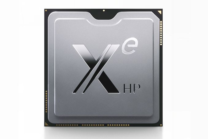
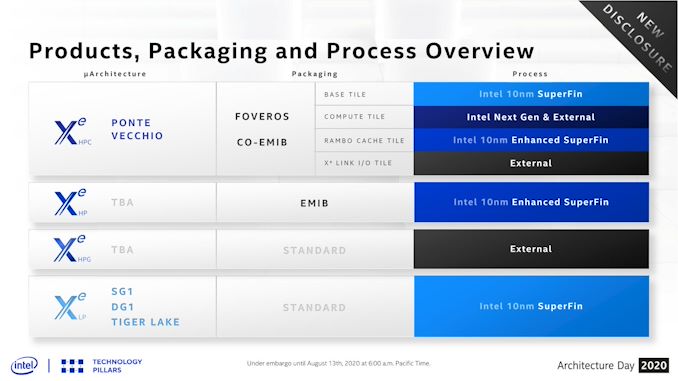
In a tweet published yesterday afternoon by Raja Koduri, Intel’s SVP and GM of the Accelerated Computing Systems and Graphics (AXG) Group, the GPU frontman revealed that Intel has dropped their plans to bring their Xe-HP series of server GPUs to the commercial market. Citing that Xe-HP has evolved into the Xe-HPC (Ponte Vecchio) and Xe-HPG (Intel Arc) families within Intel’s GPU group, the company seemingly no longer sees a need to release a second set of server GPUs – at least, not something based on Xe-HP as we know it.


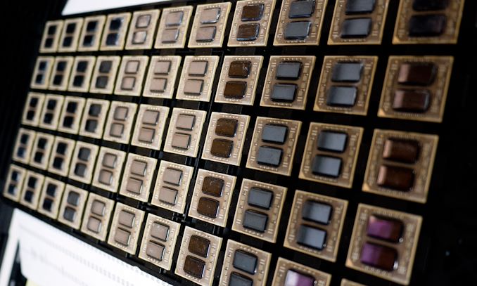
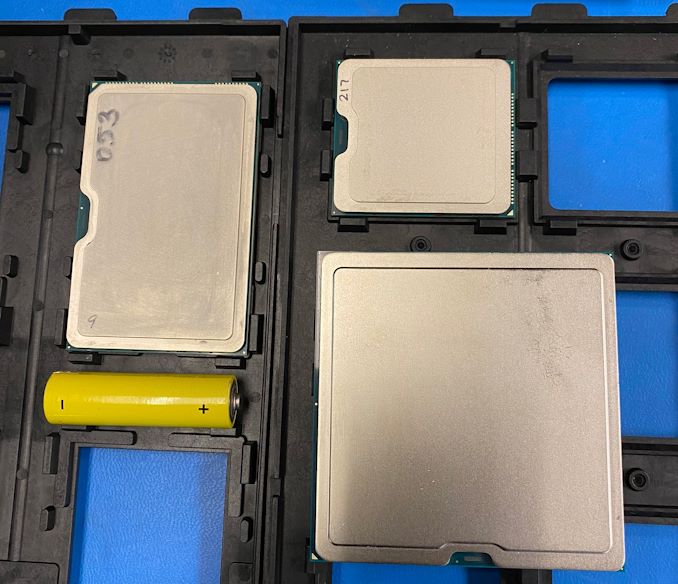
Also known by the codename Arctic Sound, Intel’s initial family of server GPUs has been the most visible product under development from Intel’s reborn GPU group. Koduri frequently showed off chips housing the silicon as it was brought-up in Intel’s labs. And, Xe-LP/DG1 excepted, this was the first high-performance Xe silicon that Intel developed. Notably, it was also the only high-performance Xe silicon slated to be manufactured by Intel; Xe-HPC’s compute tiles and Xe-HPG dies are both being built by TSMC.


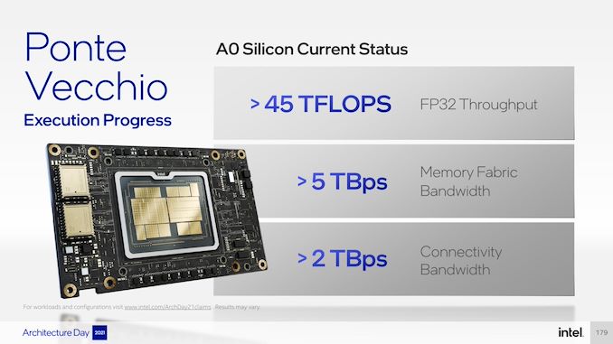
We haven’t heard much of Xe-HP this year, and in retrospect that was a sign that something was amiss. Still, as of year Intel had been showing off Xe-HP demos with performance as high as 42 TFLOPS of FP32 throughput. And in November the company announced that Xe-HP was sampling to select customers.


But, as it would seem, Xe-HP just isn’t meant to be. For 2021 Intel has been focused on getting Ponte Vecchio assembled for the Aurora supercomputer (and eventually other customers), as well as bringing up the Xe-HPG Alchemist GPU family for Q1 of 2022. According to Koduri, Xe-HP has been leveraged as a development vehicle for Aurora and Intel’s oneAPI – so it hasn’t gone unused – but that’s as far as Xe-HP has made it.


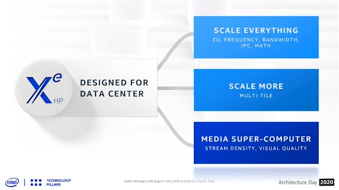
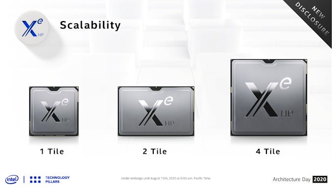
For now, the cancellation of Xe-HP raises some big questions about Intel’s server GPU plans. Xe-HP was intended to be the backbone of their server efforts, utilizing a scalable design that could range from one to four cores to serve datacenter needs ranging from compute to media processing. Between Xe-HP and Ponte Vecchio covering the very high end of the market (e.g. HPC), Intel was slated to develop a potent slate of parallel processors to compete with market-leader NVIDIA, and offer traditional Intel customers a GPU option that let them stay in Intel’s ecosystem.


At this point it’s not clear what will fill the void left by Xe-HP in Intel’s product stack. Ponte Vecchio is in production now, and judging from Intel’s revised Aurora figures, is performing better than expected. But the massive chip is expensive to build – at least in its current configuration. And while Xe-HPG could be called up for server use next year, unless Intel is able to tile it like Xe-HP, they won’t be able to offer the kind of performance that Xe-HP was slated to deliver.


Equally nebulous is a full understanding of why Intel opted to cancel Xe-HP. With the silicon already up and running, canceling it certainly sets back their server GPU plans. But as AMD has already begun rolling out their new CDNA2 architecture-based server GPU products, and NVIDIA is likely aiming for some kind of refresh of their own in 2022, there’s certainly the question of whether Xe-HP was simply too late and/or too slow to compete in the server market. Coupled with that, it’s the only lineup of high-performance Xe parts that Intel was fabbing themselves, using the 10nm Enhanced Superfin process (now referred to as Intel 7).


In any case, Intel is clearly not giving up on their plans to break into the server GPU market, even if pieces of that plan now need to be rewritten. We’ve reached out to Intel for additional details, and we’ll update this story further if Intel releases a more detailed statement on their server GPU plans.


Source: AnandTech – Intel Cans Xe-HP Server GPU Products, Shifts Focus To Xe-HPC and Xe-HPG

OWC Envoy Pro Elektron Rugged IP67 Portable SSD Review

The market for portable SSDs has expanded significantly over the past few years. With USB 3.2 Gen 2 (10 Gbps) becoming the de-facto standard for USB ports even in entry-level systems, external storage devices using the interface have flooded the market.

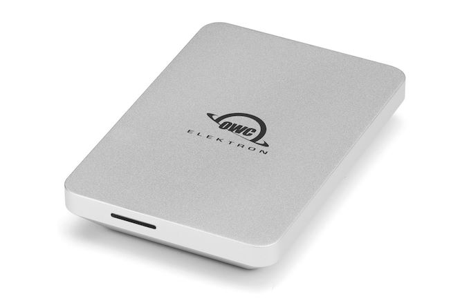
OWC has established itself as vendor of computing peripherals and upgrade components (primarily for the Apple market) over the last 30 years. Their portable SSDs lineup, under the Envoy brand, includes both Thunderbolt and USB-C offerings. The Envoy Pro EX Thunderbolt 3 and the Envoy Pro EX USB-C coupled leading performance numbers with a sleek and stylish industrial design. Late last year, the company introduced the OWC Envoy Pro Elektron – a portable flash drive similar to the Envoy Pro EX USB-C in performance, albeit in a much smaller form-factor.

Read on for our hands-on review of the Envoy Pro Elektron to check out how it fares in our updated test suite for direct-attached storage devices.


Source: AnandTech – OWC Envoy Pro Elektron Rugged IP67 Portable SSD Review

European Union Regulators Open Probe Into NVIDIA-Arm Acquisition

Following an extended period of regulatory uncertainly regarding NVIDIA’s planned acquisition of Arm, the European Union executive branch, the European Commission, has announced that they have opened up a formal probe into the deal. Citing concerns about competition and the importance of Arm’s IP, the Commission has kicked off a 90 day review process for the merger to determine if those concerns are warranted, and thus whether the merger should be modified or blocked entirely. Given the 90 day window, the Commission has until March 15th of 2022 to publish a decision.


At a high level, the EC’s concerns hinge around the fact that Arm is an IP supplier for both NVIDIA and its competitors. Which has led the EC to be concerned about whether NVIDIA would use its ownership of Arm to limit or otherwise degrade competitors’ access to Arm’s IP. This is seen as an especially concerning scenario given the breadth of device categories that Arm chips are in – everything from toasters to datacenters. As well, the EC will also be examining whether the merger could lead to NVIDIA prioritizing the R&D of IP that NVIDIA makes heavy use of (e.g. datacenter CPUs) to the detriment of other types of IP that are used by other customers.


It is worth noting that this is going to be a slightly different kind of review than usual for the EC. Since NVIDIA and Arm aren’t competitors – something even the EC notes – this isn’t a typical competitive merger. Instead, the investigation is going to be all about the downstream effects of a major supplier also becoming a competitor.


Overall, the need for a review is not terribly surprising. Given the scope of the $40 billion deal, the number of Arm customers (pretty much everyone), and the number of countries involved (pretty much everyone again), there was always a good chance that the deal could be investigated by one or more nations. Still, the EC’s investigation means that, even if approved, the deal will almost certainly not close by March as previously planned.

“Semiconductors are everywhere in products and devices that we use everyday as well as in infrastructure such as datacentres. Whilst Arm and NVIDIA do not directly compete, Arm’s IP is an important input in products competing with those of NVIDIA, for example in datacentres, automotive and in Internet of Things. Our analysis shows that the acquisition of Arm by NVIDIA could lead to restricted or degraded access to Arm’s IP, with distortive effects in many markets where semiconductors are used. Our investigation aims to ensure that companies active in Europe continue having effective access to the technology that is necessary to produce state-of-the-art semiconductor products at competitive prices.”

Executive Vice-President Margrethe Vestager


Source: AnandTech – European Union Regulators Open Probe Into NVIDIA-Arm Acquisition

Intel's Aurora Supercomputer Now Expected to Exceed 2 ExaFLOPS Performance

As part of Intel’s 2021 Innovation event, the company offered a brief update on the Aurora supercomputer, which Intel is building for Argonne National Laboratory. The first of the US’s two under-construction exascale supercomputers, Aurora and its critical processors are finally coming together, allowing Intel to finally narrow its performance projections. As it turns out, the 1-and-change exaFLOPS system is going to be more like a 2 exaFLOPS system – Aurora’s performance is coming in high enough that Intel now expects the system to exceed 2 exaFLOPS of double precision compute performance.


Planned to be the first of the US’s two public exascale systems, the Aurora supercomputer has been through a tumultuous development process. The contract was initially awarded to Intel and Cray back in 2015 for a pre-exascale system based on Intel’s Xeon Phi accelerators, a plan that went out the window when Intel discontinued Xeon Phi development. In its place, the Aurora contract was renegotiated to become an exascale system based on a combination of Intel’s Xeon CPUs and what became their Ponte Vecchio Xe-HPC GPUs. Since then, Intel has been working down to the wire on getting the necessary silicon built in order to make a delivery window that’s already shifted from 2020 to 2021 to 2022(ish), going as far as fabbing parts of Ponte Vecchio on rival TSMC’s 5nm process.


But there is finally light at the end of the tunnel, it would seem. As Intel pushes to complete the system, its performance is coming in ahead of expectations. According to the chip company, they now expect that the assembled supercomputer will be able to deliver over 2 exaFLOPS of double precision (FP64) performance. The system previously didn’t have a specific performance figure attached to it, beyond the fact that it would be over 1 exaFLOPS in FP64 throughput.


This higher performance figure for Aurora comes courtesy of Ponte Vecchio, which according to CEO Pat Gelsinger is overdelivering on performance. Gelsinger hasn’t gone into additional detail in how Ponte Vecchio is overdelivering, but given that IPC and overall efficiency tends to be relatively easy to nail down during simulations, the most likely candidate here is that Ponte Vecchio’s is clocking higher than Intel’s previous projections. Ponte Vecchio is one of the first HPC chips (and the first Intel GPU) built on TSMC’s N5 process, so there have been a lot of unknowns going into this project.


For Intel, this is no doubt a welcome bit of good luck for a project that has seen many hurdles. The repeated delays have already allowed rival AMD to get the honors of delivering the first exascale system with Frontier, which is currently being installed and is expected to offer 1.5 exaFLOPS in performance. So while Intel no longer gets to be first, once Aurora does come online next year, it will be the faster of the two systems.


Source: AnandTech – Intel’s Aurora Supercomputer Now Expected to Exceed 2 ExaFLOPS Performance

Intel 12th Gen Core Alder Lake for Desktops: Top SKUs Only, Coming November 4th

Over the past few months, Intel has been drip-feeding information about its next-generation processor family. Alder Lake, commercially known as Intel’s 12th Generation Core architecture, is officially being announced today for a November 4th launch. Alder Lake contains Intel’s latest generation high-performance cores combined with new high-efficiency cores for a new hybrid design, along with updates to Windows 11 to improve performance with the new heterogeneous layout. Only the six high-performance K and KF processor variants are coming this side of the New Year, with the rest due for Q1. We have specifications, details, and insights ahead of the product reviews on November 4th.


Source: AnandTech – Intel 12th Gen Core Alder Lake for Desktops: Top SKUs Only, Coming November 4th

AMD Reports Q3 2021 Earnings: Records All Around

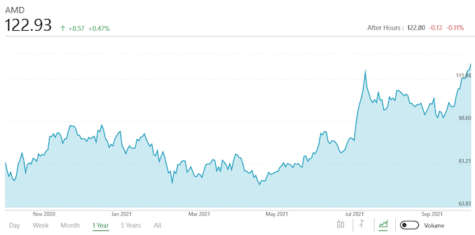
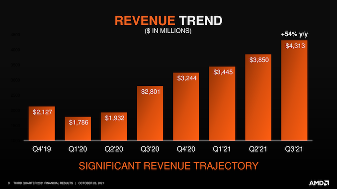
Continuing our earnings season coverage for Q3’21, today we have the yin to Intel’s yang, AMD. The number-two x86 chip and discrete GPU maker has been enjoying explosive growth ever since AMD kicked off its renaissance of sorts a couple of years ago, and that trend has been continuing unabated – AMD is now pulling in more revenue in a single quarter than they did in all of 2016. Consequently, AMD has been setting various records for several quarters now, and their latest quarter is no exception, with AMD setting new high water marks for revenue and profitability.


For the third quarter of 2021, AMD reported $4.3B in revenue, making a massive 54% jump over a year-ago quarter for AMD, when the company made just $2.8B in a then-record quarter. That makes Q3’21 both the best Q3 and the best quarter ever for the company, continuing a trend that has seen the company’s revenue grow for the last 6 quarters straight – and this despite a pandemic and seasonal fluctuations.


As always, AMD’s growing revenues have paid off handsomely for the company’s profitability. For the quarter, the company booked $923M in net income – coming within striking distance of their first $1B-in-profit quarter. This is a 137% increase over the year-ago quarter, underscoring how AMD’s profitability has been growing even faster than their rapidly rising revenues. Helping AMD out has been a strong gross margin for the company, which has been holding at 48% over the last two quarters.


AMD Q3 2021 Financial Results (GAAP)
  Q3’2021 Q3’2020 Q2’2021 Y/Y
Revenue $4.3B $2.8B $3.45B +54%
Gross Margin 48% 44% 48% +4pp
Operating Income $948M $449M $831M +111%
Net Income $923M $390M $710M +137%
Earnings Per Share $0.75 $0.32 $0.58 +134%


Breaking down AMD’s results by segment, we start with Computing and Graphics, which encompasses their desktop and notebook CPU sales, as well as their GPU sales. That division booked $2.4B in revenue for the quarter, $731M (44%) more than Q2 2021. Accordingly, the segment’s operating income is up quite a bit as well, going from $384M a year ago to $513M this year. Though, in a mild surprise, it is down on a quarterly basis, which AMD is ascribing to higher operating expenses.


As always, AMD doesn’t provide a detailed breakout of information from this segment, but they have provided some selective information on revenue and average selling prices (ASPs). Overall, client CPU sales have remained strong; client CPU ASPs are up on both a quarterly and yearly basis, indicating that AMD has been selling a larger share of high-end (high-margin) parts – or as AMD likes to call it, a “richer mix of Ryzen processor sales”. For their earnings release AMD isn’t offering much commentary on laptop versus desktop sales, but it’s noteworthy that the bulk of the company’s new consumer product releases in the quarter were desktop-focused, with the Radeon RX 6600 XT and Ryzen 5000G-series APUs.


Speaking of GPUs, AMD’s graphics and compute processor business is booming as well. As with CPUs, ASPs for AMD’s GPU business as up on both a yearly and quarterly basis, with graphics revenue more than doubling over the year-ago quarter. According to the company this is being driven by both high-end Radeon sales as well as AMD Instinct sales, with data center graphics revenue more than doubling on both a yearly and quarterly basis. AMD began shipping their first CDNA2-based accelerators in Q2, so for Q3 AMD has been enjoying that ramp-up as they ship out the high-margin chips for the Frontier supercomputer.


AMD Q3 2021 Reporting Segments
  Q3’2021 Q3’2020 Q2’2021

Computing and Graphics

Revenue $2398M $1667M $2250M
Operating Income $513M $384M $526M

Enterprise, Embedded and Semi-Custom

Revenue $1915M $1134M $1600M
Operating Income $542M $141M $398M


Moving on, AMD’s Enterprise, Embedded, and Semi-Custom segment has yet again experienced a quarter of rapid growth, thanks to the success of AMD’s EPYC processors and demand for the 9th generation consoles. This segment of the company booked $1.9B in revenue, $781M (69%) more than what they pulled in for Q3’20, and 20% ahead of an already impressive Q2’21. The gap between the CG and EESC groups has also further closed – the latter is now only behind AMD’s leading group by $483M in revenue.


And while AMD intentionally doesn’t separate server sales from console sales in their reporting here, the company has confirmed that both are up. AMD’s Milan server CPUs, which were launched earlier this quarter, have become the majority of AMD’s server revenue, pushing them to their 6th straight quarter of record server processor revenue. And semi-custom revenue – which is primarily the game consoles – is up not only on a yearly basis, but on a quarterly basis as well, with AMD confirming that they have been able to further expand their console APU production.


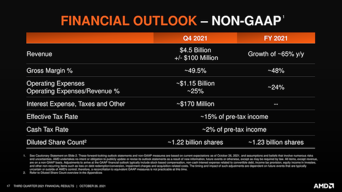
Looking forward, AMD’s expectations for the fourth quarter and for the rest of the year have been bumped up yet again. For Q4 the company expects to book a record $4.5B (+/- $100M) in revenue, which if it comes to pass will be 41% growth over Q4’20. AMD is also projecting a 49.5% gross margin for Q4, which if they exceed it even slightly, would be enough to push them to their first 50% gross margin quarter in company history. Meanwhile AMD’s full year 2021 projection now stands at a 65% year-over-year increase in revenue versus their $9.8B FY2020, which is 5 percentage points higher than their forecast from the end of Q2.


As for AMD’s ongoing Xilinx acquisition, while the company doesn’t have any major updates on the subject, they are confirming that they’re making “good progress” towards securing the necessary regulatory approvals. To that they, they are reiterating that it remains on-track to close by the end of this year.


Finally, taking a break from growing the company by 50% every year, AMD is scheduled to hold their AMD Accelerated Data Center Premiere event on Monday, November 8th. While AMD isn’t giving up too much information in advance, the company is confirming that we’ll hear more about their CDNA2 accelerator architecture, which along with the current Frontier supercomputer, will be going into their next generation Radeon Instinct products. As well, the company will also be delivering news on their EPYC server processors, which were just recently updated back in March with the launch of the 3rd generation Milan parts. As always, AnandTech will be virtually there, covering AMD’s announcements in detail, so be sure to drop by for that.


Source: AnandTech – AMD Reports Q3 2021 Earnings: Records All Around

AnandTech Interviews Mike Clark, AMD’s Chief Architect of Zen

AMD is calling this time of the year as its ‘5 years of Zen’ time, indicating that back in 2016, it was starting to give the press the first taste of its new microarchitecture which, in hindsight, ultimately saved the company. How exactly Zen came to fruition has been slyly hidden from view all these years, with some of the key people popping up from time to time: Jim Keller, Mike Clark, and Suzanne Plummer hitting the headlines more often than most. But at the time AMD started to disclose details about the design, it was Mike Clark front and center in front of those slides. At the time I remember asking him for all the details, but as part of the 5 Year messaging, offered Mike for a formal interview on the topic.


Source: AnandTech – AnandTech Interviews Mike Clark, AMD’s Chief Architect of Zen

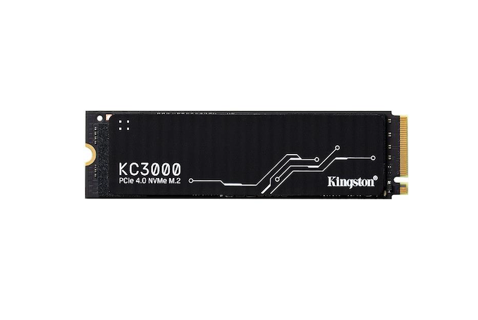
Kingston KC3000 PCIe 4.0 NVMe Flagship SSD Hits Retail

Kingston had previewed their 2021 flagship PCIe 4.0 x 4 M.2 NVMe SSD (codename “Ghost Tree”) at CES earlier this year. Not much was divulged other than the use of the Phison E18 controller at that time. The product is hitting retail shelves today as the KC3000. The M.2 2280 SSD will be available in four capacities ranging from 512GB to 4TB. Kingston also provided us with detailed specifications.


Kingston KC3000 SSD Specifications
Capacity 512 GB 1024 GB 2048 GB 4096 GB
Controller Phison E18
NAND Flash Micron 176L 3D TLC NAND
Form-Factor, Interface Single-Sided M.2-2280, PCIe 4.0 x4, NVMe 1.4 Double-Sided M.2-2280, PCIe 4.0 x4, NVMe 1.4
DRAM 512 MB DDR4 1 GB DDR4 2 GB DDR4 4 GB DDR4
Sequential Read 7000 MB/s
Sequential Write 3900 MB/s 6000 MB/s 7000 MB/s
Random Read IOPS 450K 900K 1M
Random Write IOPS 900K 1M
Avg. Power Consumption 0.34 W 0.33 W 0.36 W
Max. Power Consumption 2.7 W (R)

4.1 W (W)
2.8 W (R)

6.3 W (W)
2.8 W (R)

9.9 W (W)
2.7 W (R)

10.2 W (W)
SLC Caching Yes
TCG Opal Encryption No
Warranty 5 years
Write Endurance 400 TBW

0.44 DWPD
800 TBW

0.44 DWPD
1600 TBW

0.44 DWPD
3200 TBW

0.44 DWPD
MSRP ? (?¢/GB) ? (?¢/GB) ? (?¢/GB) ? (?¢/GB)


SSDs based on Phison’s E18 controller have been entering the market steadily over the last few months. While early ones like the Sabrent Rocket 4 Plus and Mushkin Gamma Gen 4 came with Micron’s 96L flash, the newer ones such as the Corsair MP600 PRO XT and the Kingston’s KC3000 are using 176L NAND. The KC3000’s 0.44 DWPD endurance rating slightly edges ahead of the MP600 PRO XT’s 0.38 DWPD despite similar component choices. Claimed performance numbers are similar to ones achieved by other E18 SSDs with similar NAND configuration – 7GBps for sequential accesses, and up to 1M IOPS for random accesses. The thermal solution involves an overlaid graphene aluminum heat-spreader that still keeps the thickness down to 2.21mm for the single-sided SKUs, and 3.5mm for the double-sided ones. On the power consumption side, the 4TB version can consume as much as 10.2W. On the positive side, all SKUs support a 5mW deep sleep mode.


Kingston is targeting the KC3000 towards both desktops and notebooks. Primary storage-intensive use-cases include 3D rendering and 4K content creation. In this market, the drive is going up against established competition like the Samsung 980 PRO, and Western Digital’s SN850. Both of these SSDs have lower endurance numbers and don’t have 4TB options, giving the KC3000 an edge for consumers looking at those aspects specifically.


Source: AnandTech – Kingston KC3000 PCIe 4.0 NVMe Flagship SSD Hits Retail

Apple's M1 Pro, M1 Max SoCs Investigated: New Performance and Efficiency Heights

Last week, Apple had unveiled their new generation MacBook Pro laptop series, a new range of flagship devices that bring with them significant updates to the company’s professional and power-user oriented user-base. The new devices particularly differentiate themselves in that they’re now powered by two new additional entries in Apple’s own silicon line-up, the M1 Pro and the M1 Max. We’ve covered the initial reveal in last week’s overview article of the two new chips, and today we’re getting the first glimpses of the performance we’re expected to see off the new silicon.


Source: AnandTech – Apple’s M1 Pro, M1 Max SoCs Investigated: New Performance and Efficiency Heights

The ASRock X570S PG Riptide Motherboard Review: A Wave of PCIe 4.0 Support on A Budget

Officially announced at Computex 2021, AMD and its vendors unveiled a new series of AM4 based motherboards for Ryzen 5000 processors. The new X570S chipset is, really, not that different from the previous version launched back in 2019 from a technical standpoint. The main user difference is that all of the X570S models now feature a passively cooled chipset. Some vendors have opted to either refresh existing models, or others are releasing completely new variants, such as the ASRock X570S PG Riptide we are reviewing today. Aimed at the entry-level extreme chipset, the X570S PG Riptide features a Killer-based 2.5 GbE controller, dual PCIe 4.0 x4 M.2 slots, and support for up to 128 GB of DDR4-5000.


Source: AnandTech – The ASRock X570S PG Riptide Motherboard Review: A Wave of PCIe 4.0 Support on A Budget

Intel Reports Q3 2021 Earnings: Client Down, Data Center and IoT Up

Kicking off another earnings season, Intel is once again leading the pack of semiconductor companies in reporting their earnings for the most recent quarter. As the company gets ready to go into the holiday quarter, they are coming off what’s largely been a quiet quarter for the chip maker, as Intel didn’t launch any major products in Q3. Instead, Intel’s most recent quarter has been driven by ongoing sales of existing products, with most of Intel’s business segments seeing broad recoveries or other forms of growth in the last year.


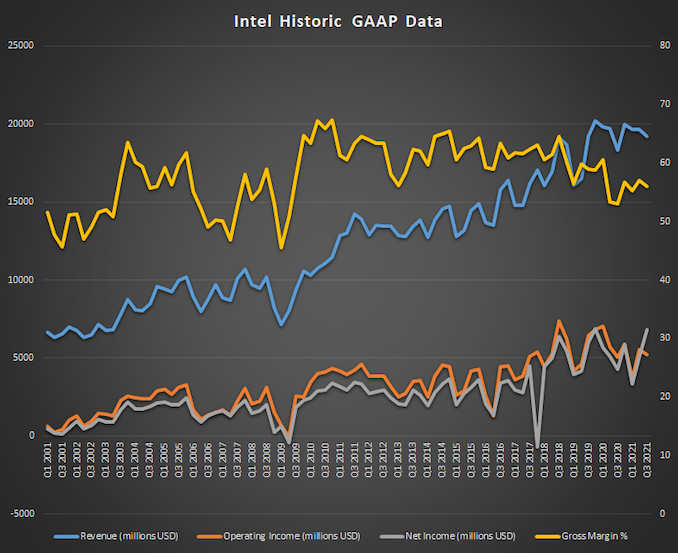
For the third quarter of 2021, Intel reported $19.2B in revenue, a $900M improvement over the year-ago quarter. Intel’s profitability has also continued to grow – even faster than overall revenues – with Intel booking $6.8B in net income for the quarter, dwarfing Q3’2020’s “mere” $4.3B. Unsurprisingly, that net income growth has been fueled in part by higher gross margins; Intel’s overall gross margin for the quarter was 56%, up nearly 3 percentage points from last year.


Intel Q3 2021 Financial Results (GAAP)
  Q3’2021 Q2’2021 Q3’2020
Revenue $19.2B $19.7B $18.3B
Operating Income $5.2B $5.7B $5.1B
Net Income $6.8B $5.1B $4.3B
Gross Margin 56.0% 53.3% 53.1%
Client Computing Group Revenue $9.7B -4% -2%
Data Center Group Revenue $6.5B flat +10%
Internet of Things Group Revenue $1.0B +2% +54%
Mobileye Revenue $326M flat +39%
Non-Volatile Memory Solutions Group $1.1B flat -4%
Programmable Solutions Group $478M -2% +16%


Breaking things down by Intel’s individual business groups, most of Intel’s groups have enjoyed significant growth over the year-ago quarter. The only groups not to report gains are Intel’s Client Computing Group (though this is their largest group) and their Non-Volatile Memory Solutions Group, which Intel is in the process of selling to SK Hynix.


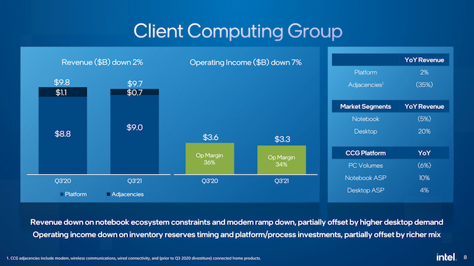
Starting with the CCG then, Intel’s core group is unfortunately also the only one struggling to grow right now. With $9.7B in revenue, it’s down just 2% from Q3’2020, but that’s something that stands out when Intel’s other groups are doing so well. Further breaking down the numbers, platform revenue overall is actually up 2% on the year, but non-platform revenue – “adjacencies” as Intel terms them, such as their modem and wireless communications product lines – are down significantly. On the whole this isn’t too surprising since Intel is in the process of winding down its modem business anyhow as part of that sale to Apple, but it’s an extra drag that Intel could do without.


The bigger thorn in Intel’s side at the moment, according to the company, is the ongoing chip crunch, which has limited laptop sales. With Intel’s OEM partners unable to source enough components to build as many laptops as they’d like, it has the knock-on effect of reducing their CPU orders, even though Intel itself doesn’t seem to be having production issues. The upshot, at least, is that desktop sales are up significantly versus the year-ago quarter, and that average selling prices (ASPs) for both desktop and notebook chips are up.


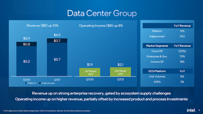
Meanwhile, Intel’s Data Center Group is enjoying a recovery in enterprise spending, pushing revenues higher. DCG’s revenue grew 10% year-over-year, with both sales volume and ASPs increasing by several percent on the back of their Ice Lake Xeon processors. A bit more surprising here is that Intel believes they could be doing even better if not for the chip crunch; higher margin products like servers are typically not impacted as much by these sorts of shortages, since server makers have the means to pay for priority.


Unfortunately, unlike Q2 Intel isn’t providing a quarter-over-quarter (i.e. vs the previous quarter) figures for their breakdowns. So while overall DCG revenue is flat on a quarterly basis, it sounds like Intel hasn’t really recovered from the hit they took in Q2. Meanwhile, commerntary on Intel’s earnings call suggests the sales of the largest (XCC) Ice Lake Xeons has been softer than Intel first expected, which has kept ASP growth down in an otherwise DCG-centric quarter.


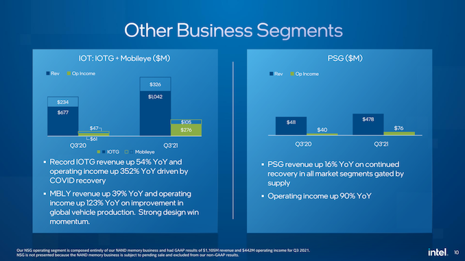
The third quarter was also kind to Intel’s IoT groups and their Programmable Solutions Group. All three groups are up by double-digit percentages on a YoY basis, particularly the Internet of Things Group (IoTG), which is up 54%. According to Intel, that IOTG growth is largely due to businesses recovering from the pandemic, with a similar story for the Mobileye group thanks to automotive production having ramped back up versus its 2020 lows.


Otherwise, Intel’s final group, the Non-Volatile Memory Solutions Group, was the other declining group for the quarter. At this point Intel has officially excised the group’s figures from their non-GAAP reporting, and while they’re still required to report those figures in GAAP reports, they aren’t further commenting on a business that will soon no longer be theirs.


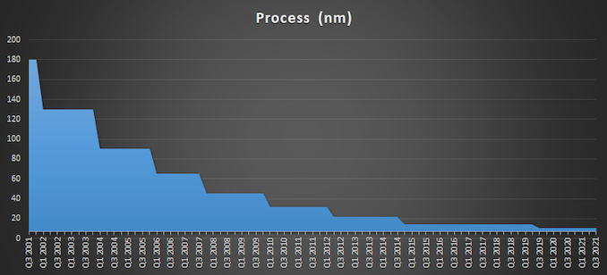
Finally, tucked inside Intel’s presentation deck is an interesting note: Intel Foundry Services (IFS) has shipped its first revenue wafers. Intel is, of course, betting heavily on IFS becoming a cornerstone of its overall chip-making business in the future as part of its IDM 2.0 strategy, so shipping customers’ chips for revenue is an important first step in that process. Intel has laid out a very aggressive process roadmap leading up to 20A in 2024, and IFS’s success will hinge on whether they can hit those manufacture ring technology targets.


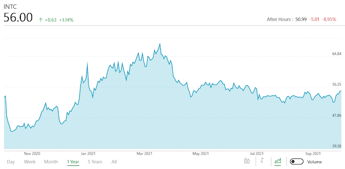
For Intel, Q3’2021 was overall a decent quarter for the group – though what’s decent is relative. With the DCG, IOTG, and Mobileye groups all setting revenue records for the quarter (and for IOTG, overall records), Intel continues to grow. On the flip side, however, Intel missed their own revenue projections for the quarter by around $100M, so in that respect they’ve come in below where they intended to be. And judging from the 7% drop in the stock price during after-hours trading, investors are taking note.


Looking forward, Intel is going into the all-important Q4 holiday sales period, typically their biggest quarter of the year. At this point the company is projecting that it will book $18.3B in non-GAAP revenue (excluding NSG), which would be a decline of 5% versus Q4’2020. Similarly, the company is expecting gross margins to come back down a bit, forecasting a 53.5% margin for the quarter. On the product front, Q4 will see the launch of the company’s Alder Lake family of processors, though initial CPU launches and their relatively low volumes tend not to move the needle too much.


On that note, Intel’s Innovation event is scheduled to take place next week, on the 27th and 28th. The two day event is a successor-of-sorts to Intel’s IDF program, and we should find out more about the Alder Lake architecture and Intel’s specific product plans at that time.


Source: AnandTech – Intel Reports Q3 2021 Earnings: Client Down, Data Center and IoT Up

Intel Reaffirms: Our Discrete GPUs Will Be On Shelves in Q1 2022

Today is when Intel does its third-quarter 2021 financial disclosures, and there’s one little tidbit in the earnings presentation about its upcoming new discrete GPU offerings. The earnings are usually a chance to wave the flag of innovation about what’s to come, and this time around Intel is confirming that its first-generation discrete graphics with the Xe-HPG architecture will be on shelves in Q1 2022.


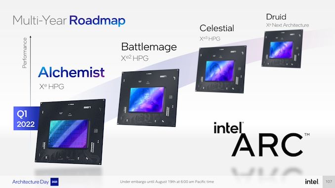
Intel has slowly been disclosing the features for its discrete gaming graphics offerings. Earlier this year, the company announced the branding for its next-gen graphics, called Arc, and with that the first four generations of products: Alchemist, Battlemage, Celestial, and Druid. It’s easy to see that we’re going ABCD here. Technically at that disclosure, in August 2021, Intel did state that Alchemist will be coming in Q1, the reaffirmation of the date today in the financial disclosures indicates that they’re staying as close to this date as possible.


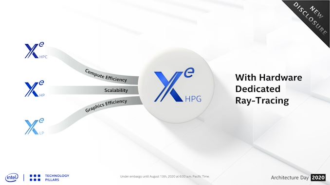
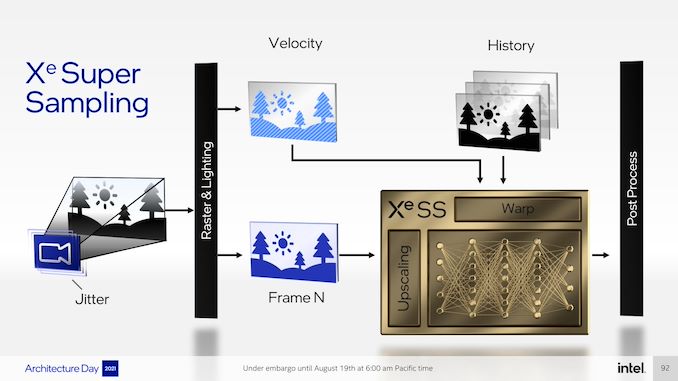
Intel has previously confirmed that Alchemist will be fully DirectX 12 Ultimate compliant – meaning that alongside RT, it will offer variable-rate shading, mesh shaders, and sampler feedback. This will make it comparable in core graphics features to current-generation AMD and NVIDIA hardware. Although it has taken a few years now to come to fruition, Intel has made it clear for a while now that the company has intended to become a viable third player in the discrete graphics space. Intel’s odyssey, as previous marketing efforts have dubbed it, has been driven primarily by developing the Xe family of GPU microarchitectures, as well as the GPUs based on those architectures. Xe-LP was the first out the door last year, as part of the Tiger Lake family of CPUs and the DG1 discrete GPU. Other Xe family architectures include Xe-HP for servers and Xe-HPC for supercomputers and other high-performance compute environments.


The fundamental building block of Alchemist is the Xe Core. For manufacturing, Intel is turning to TSMC’s N6 process to do it. Given Intel’s Q1’22 release timeframe, Intel’s Alchemist GPUs will almost certainly be the most advanced consumer GPUs on the market with respect to manufacturing technology. Alchemist will be going up against AMD’s Navi 2x chips built on N7, and NVIDIA’s Ampere GA10x chips built on Samsung 8LPP. That said, as AMD can attest to, there’s more to being competitive in the consumer GPU market than just having a better process node. In conjunction with the use of TSMC’s N6 process, Intel is reporting that they’ve improved both their power efficiency (performance-per-watt) and their clockspeeds at a given voltage by 50% compared to Xe-LP. Note that this is the sum total of all of their improvements – process, logic, circuit, and architecture – so it’s not clear how much of this comes from the jump to TSMC N6 from Intel 10SF, and how much comes from other optimizations.


Exactly what performance level and pricing Intel will be pitching its discrete graphics to is currently unknown. The Q1 launch window puts CES (held the first week of January) as a good spot to say something more.


Related Reading


Source: AnandTech – Intel Reaffirms: Our Discrete GPUs Will Be On Shelves in Q1 2022

SK Hynix Announces Its First HBM3 Memory: 24GB Stacks, Clocked at up to 6.4Gbps

Though the formal specification has yet to be ratified by JEDEC, the memory industry as a whole is already gearing up for the upcoming launch of the next generation of High Bandwidth Memory, HBM3. Following announcements earlier this summer from controller IP vendors like Synopsys and Rambus, this morning SK Hynix is announcing that it has finished development of its HBM3 memory technology – and according to the company, becoming the first memory vendor to do so. With controller IP and now the memory itself nearing or at completion, the stage is being set for formal ratification of the standard, and eventually for HBM3-equipped devices to start rolling out later in 2022.


Overall, the relatively lightweight press release from SK Hynix is roughly equal parts technical details and boasting. While there are only 3 memory vendors producing HJBM – Samsung, SK Hynix, and Micron – it’s still a technically competitive field due to the challenges involved in making deep-stacked and TSV-connected high-speed memory work, and thus there’s a fair bit of pride in being first. At the same time, HBM commands significant price premiums even with its high production costs, so memory vendors are also eager to be first to market to cash in on their technologies.


In any case, both IP and memory vendors have taken to announcing some of their HBM wares even before the relevant specifications have been announced. We saw both parties get an early start with HBM2E, and now once again with HBM3. This leaves some of the details of HBM3 shrouded in a bit of mystery – mainly that we don’t know what the final, official bandwidth rates are going to be – but announcements like SK Hynix’s help narrow things down. Still, these sorts of early announcements should be taken with a small grain of salt, as memory vendors are fond of quoting in-lab data rates that may be faster than what the spec itself defines (e.g. SK Hynix’s HBM2E).


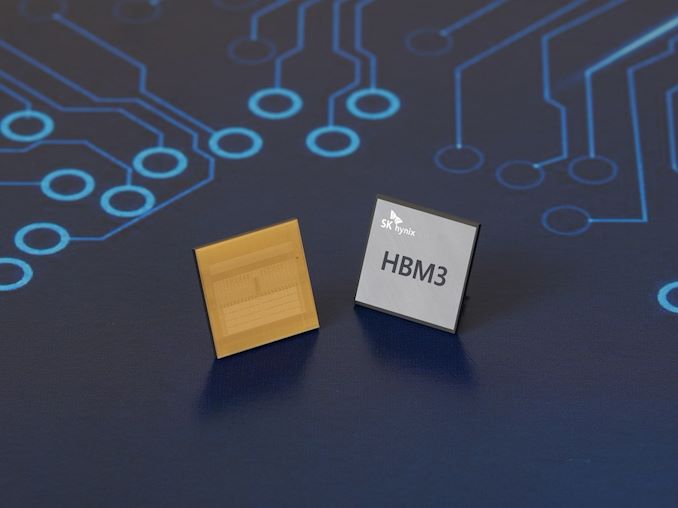
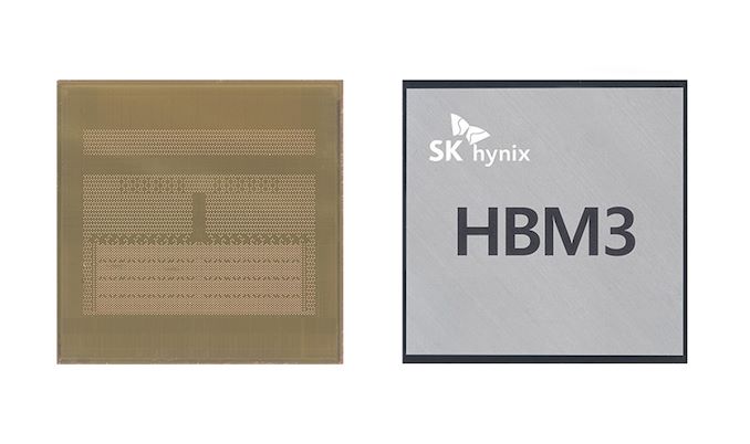
Getting into the technical details, according to SK Hynix their HBM3 memory will be able to run as fast as 6.4Gbps/pin. This would be double the data rate of today’s HBM2E, which formally tops out at 3.2Gbps/pin, or 78% faster than the company’s off-spec 3.6Gbps/pin HBM2E SKUs. SK Hynix’s announcement also indirectly confirms that the basic bus widths for HBM3 remain unchanged, meaning that a single stack of memory is 1024-bits wide. At Hynix’s claimed data rates, this means a single stack of HBM3 will be able to deliver 819GB/second worth of memory bandwidth.


SK Hynix HBM Memory Comparison
  HBM3 HBM2E HBM2
Max Capacity 24 GB 16 GB 8 GB
Max Bandwidth Per Pin 6.4 Gb/s 3.6 Gb/s 2.0 Gb/s
Number of DRAM ICs per Stack 12 8 8
Effective Bus Width 1024-bit
Voltage ? 1.2 V 1.2 V
Bandwidth per Stack 819.2 GB/s 460.8 GB/s 256 GB/s


SK Hynix will be offering their memory in two capacities: 16GB and 24GB. This aligns with 8-Hi and 12-Hi stacks respectively, and means that at least for SK Hynix, their first generation of HBM3 memory is still the same density as their latest-generation HBM2E memory. This means that device vendors looking to increase their total memory capacities for their next-generation parts (e.g. AMD and NVIDIA) will need to use memory with 12 dies/layers, up from the 8 layer stacks they typically use today.


What will be interesting to see in the final version of the HBM3 specification is whether JEDEC sets any height limits for 12-Hi stacks of HBM3. The group punted on the matter with HBM2E, where 8-Hi stacks had a maximum height but 12-Hi stacks did not. That in turn impeded the adoption of 12-Hi stacked HBM2E, since it wasn’t guaranteed to fit in the same space as 8-Hi stacks – or indeed any common size at all.


On that matter, the SK Hynix press release notably calls out the efforts the company put into minimizing the size of their 12-Hi (24GB) HBM3 stacks. According to the company, the dies used in a 12-Hi stack – and apparently just the 12-Hi stack – have been ground to a thickness of just 30 micrometers, minimizing their thickness and allowing SK Hynix to properly place them within the sizable stack. Minimizing stack height is beneficial regardless of standards, but if this means that HBM3 will require 12-Hi stacks to be shorter – and ideally, the same height as 8-Hi stacks for physical compatibility purposes – then all the better for customers, who would be able to more easily offer products with multiple memory capacities.


Past that, the press release also confirms that one of HBM’s core features, integrated ECC support, will be returning. The standard has offered ECC since the very beginning, allowing device manufacturers to get ECC memory “for free”, as opposed to having to lay down extra chips with (G)DDR or using soft-ECC methods.


Finally, it looks like SK Hynix will be going after the same general customer base for HBM3 as they already are for HBM2E. That is to say high-end server products, where the additional bandwidth of HBM3 is essential, as is the density. HBM has of course made a name for itself in server GPUs such as NVIDIA’s A100 and AMD’s M100, but it’s also frequently tapped for high-end machine learning accelerators, and even networking gear.


We’ll have more on this story in the near future once JEDEC formally approves the HBM3 standard. In the meantime, it’s sounding like the first HBM3 products should begin landing in customers’ hands in the later part of next year.


Source: AnandTech – SK Hynix Announces Its First HBM3 Memory: 24GB Stacks, Clocked at up to 6.4Gbps

The Huawei MateBook 16 Review, Powered by AMD Ryzen 7 5800H: Ecosystem Plus

Having very recently reviewed the Matebook X Pro 2021 (13.9-inch), our local PR in the UK offered me a last-minute chance to examine the newest element to their laptop portfolio. The Huawei MateBook 16, on paper at least, comes across as a workhorse machine designed for office and on the go. A powerful CPU that can go into a high-performance mode when plugged in, and sip power when it needs to. No discrete graphics to get in the way, and a massive 84 Wh battery is designed for an all-day workflow. It comes with a color-accurate large 3:2 display, and with direct screen share with a Huawei smartphone/tablet/monitor, it means if you buy into the ecosystem there’s a lot of potential. The question remains – is it any good?


Source: AnandTech – The Huawei MateBook 16 Review, Powered by AMD Ryzen 7 5800H: Ecosystem Plus

Google Announces Pixel 6, Pixel 6 Pro: The New Real Flagship Pixels

Today, after many weeks, even months of leaks and teasers, Google has finally announced the new Pixel 6 and Pixel 6 Pro – their new flagship line-up of phones for 2021 and carrying them over into next year. The two phones had been teased quite on numerous occasions and have probably one of the worst leak records of any phone ever, and today’s event revealed little unknowns, but yet still Google manages to put on the table a pair of very interesting phones, if not, the most interesting Pixel phones the company has ever managed to release.


Source: AnandTech – Google Announces Pixel 6, Pixel 6 Pro: The New Real Flagship Pixels

The Arm DevSummit 2021 Keynote Live Blog: 8am PT (15:00 UTC)

This week seems to be Arm’s week across the tech industry. Following yesterday’s Arm SoC announcements from Apple, today sees Arm kick off their 2021 developer’s summit, aptly named DevSummit. As always, the show is opening up with a keynote being delivered by Arm CEO Simon Segars, who will be using the opportunity to lay out Arm’s vision of the future.


Arm chips are already in everything from toasters to PCs – and Arm isn’t stopping there. So be sure to join us at 8am PT (15:00 UTC) for our live blog coverage of Arm’s keynote.


Source: AnandTech – The Arm DevSummit 2021 Keynote Live Blog: 8am PT (15:00 UTC)