The SilverStone NightJar NJ700 Passive PSU Review: Silent Excellence

In today’s review we are taking a look at a passively cooled power supply, the SilverStone Nightjar NJ700. Despite the lack of active cooling, the NJ700 can continuously output up to 700 Watts, underscoring its very high efficiency as well as the rest of its impressive electrical specifications. Thanks to it’s impeccable design and component selection – courtesy of OEM SeaSonic – the overall performance of the Nightjar NJ700 is world-class, making it more than a match for the even the vast majority of actively cooled 700W PSUs on the market today. Just don’t expect one of the best PSUs we’ve ever reviewed to come cheaply.


Source: AnandTech – The SilverStone NightJar NJ700 Passive PSU Review: Silent Excellence

Texas To Get Multiple New Fabs as Samsung and TI to Spend $47 Billion on New Facilities

After a year of searching for the right place of its new U.S. fab, Samsung this week announced that it would build a fab near Taylor, Texas. The company will invest $17 billion in the new semiconductor fabrication plant and will receive hundreds of millions of dollars in incentives from local and state authorities. Separately, Texas authorities have announced that Texas Instruments intend to spend $30 billion on new fabs in the state, as well.


Samsung to Spend $17 Billion on New Texas Fab


Samsung yet has to disclose all the details about its fab near Taylor, Texas, but for now the company says that the new fab site will occupy an area of over 5 million square meters and will employ 2,000 workers directly and another 7,000 indirectly. To put the number into context, Samsung’s fab near Austin, Texas currently employs about 10,000 of workers. 


Samsung will start construction of the new fab in the first half of 2022 and expects it to be operational in the second half of 2024. It usually takes about a year to construct a building for a semiconductor manufacturing facility and then about a year to install and set up all the necessary equipment.


Samsung has not announced which process technologies will be used at its fab near Taylor, Texas, but says it will produce chips for 5G, artificial intelligence (AI), high-performance computing (HPC), and mobile applications, which implies that the fab will gain fairly advanced technologies. In fact, keeping in mind that all of Samsung’s nodes thinner than 7 nm rely on extreme ultraviolet (EUV) lithography, it is reasonable to expect the new fab to be EUV capable. As a result, Samsung’s customers from the U.S. (such as IBM, Nvidia, and Qualcomm) will be able to produce their chips in the U.S. rather than in South Korea, which might allow their developers to address systems used by the U.S. government. 


“With greater manufacturing capacity, we will be able to better serve the needs of our customers and contribute to the stability of the global semiconductor supply chain,” said Kinam Kim, Vice Chairman and CEO, Samsung Electronics Device Solutions Division. “In addition to our partners in Texas, we are grateful to the Biden Administration for creating an environment that supports companies like Samsung as we work to expand leading-edge semiconductor manufacturing in the U.S. We also thank the administration and Congress for their bipartisan support to swiftly enact federal incentives for domestic chip production and innovation.”


Samsung’s new semiconductor production plant will be located 25 kilometers away from the company’s fab near Austin, Texas, so the facilities will be able to share infrastructure and resources (such as materials and supplies).


Samsung says that it will spend about $6 billion on construction on the building as well as improvements of the local infrastructure. Tools that will be used by the fab will cost another $11 billion. Meanwhile, to build the new plant Samsung will receive hundreds of millions in incentives from the state, the county, and the city, according to media reports. Some of the packages have not been approved yet. 


Texas Instruments to Invest $30 Billion on New U.S. Fabs


Samsung is not the only company to build new fabs in Texas. The Governor of Texas recently announced the Texas Instruments was planning to build several new 300-mm fabs near Sherman. In total, TI intends to build as many as four wafer fabrication facilities in the region over coming decades and the cumulative investments are expected to total $30 billion as fabs will be eventually upgraded.


Texas Instruments itself yet have to formally announce its investments plans, but the announcement by the governor Greg Abbot indicates that the principal decisions have been made and now TI needs to finalize the details. 


Sources: SamsungAustin American-StatesmanTexas.gov


Source: AnandTech – Texas To Get Multiple New Fabs as Samsung and TI to Spend Billion on New Facilities

The Intel Z690 Motherboard Overview (DDR4): Over 30+ New Models

To support the launch of Intel’s latest 12th generation ‘Alder Lake’ processors, Intel has also pulled the trigger on its latest Z690 motherboard chipset. Using a new LGA1700 socket, some of the most significant advancements with Alder Lake and Z690 include PCIe 5.0 support from the processor, as well as a PCIe 4.0 x8 link from the processor to the chipset. In this article, we’re taking a closer look at over 30+ different DDR4 enabled motherboards designed to not only use the processing power of Alder Lake but offer users a myriad of high-class and premium features.


Source: AnandTech – The Intel Z690 Motherboard Overview (DDR4): Over 30+ New Models

Qualcomm x Nuvia: Silicon Sampling in Late 2022, Products in 2023

One of the more curious acquisitions in the last couple of years has been that of Nuvia by Qualcomm. Nuvia was a Silicon Valley start-up founded by the key silicon and design engineers and architects behind both Apple’s and Google’s silicon for the past few years. Qualcomm CEO Cristiano Amon made it crystal clear when Nuvia was acquired that they were going after the high-performance ultraportable laptop market, with both Intel and Apple in the crosshairs.


Nuvia came out of stealth in November 2019, with the three main founders having spent almost a year building the company. Gerard Williams III, John Bruno, and Manu Gulati have collectively driven the silicon design of 20+ chips, have combined over 100 patent, and have been in leadership roles across Google, Apple, Arm, Broadcom, and AMD. Nuvia raised a lot of capital, $300M+ over two rounds of funding and angel investors, and the company hired a lot of impressive staff.


The goal of Nuvia was to build an Arm-based general purpose server chip that would rock the industry. Imagine something similar to what Graviton 2 and Ampere Altra are today, but with a custom microarchitecture on par (or better) with Apple’s current designs. When Nuvia was still on its own in start-up mode, some were heralding the team and the prospect, calling for the downfall of x86 with Nuvia’s approach. However, Qualcomm swept in and acquired the company in March 2021, and repurposed Nuvia’s efforts towards a laptop processor.


It’s been no secret that Qualcomm has been after the laptop and notebook market for some time. Multiple generations of ‘Windows on Snapdragon’ have come to market through Qualcomm’s partners, initially featuring smartphone-class silicon before becoming something more bespoke with the 8cx, 8cx Gen 2, and 7c/7 options in the past couple of years. It has taken several years for Qualcomm to get the silicon and the Windows ecosystem somewhere that makes sense for commercial and consumer use, and with the recent news that Windows 11 on these devices now enabling full x86-64 emulation support, the functional difference between a Qualcomm laptop and an x86 laptop is supposed to be near zero. Qualcomm would argue their proposition is better, allowing for 2 days of use on a single charge, holding charge for weeks, and mobile wireless connectivity with 4G/5G. I’ve tested one of the previous generation S855 Lenovo Yoga devices, and the battery life is insane – but I needed better were functional support (turns out I have an abnormal edge-case work flow…) and more performance. While Qualcomm has been working on the former since my last test, and Nuvia is set to bring the latter.


Image from @anshelsag on Twitter, Used with permission


At Qualcomm’s Investor Day this week, the Qualcomm/Nuvia relationship was mentioned in an update. I had hoped that by the end of this year (and Qualcomm’s Tech Summit in only a couple of weeks) that we might be seeing something regarding details or performance, however Qualcomm is stating that its original schedule is still on track. As announced at the acquisition, the goal is to deliver test silicon into the hands of partners in the second half of 2022.


The goal here is to have laptop silicon that is competitive with Apple’s M-series, but running Windows. This means blowing past Intel and AMD offerings, and coupled with the benefits of better battery life, sustained performance, and mobile connectivity. From the disclosures so far, it’s perhaps no surprise that the Nuvia CPUs will be paired with an Adreno GPU and a Hexagon DSP, although it will be interesting to see if the Nuvia CPU is a single big core paired with regular Arm efficient cores, or everything in the CPU side will be new from the Nuvia team.


I have no doubt that at Qualcomm’s Tech Summit in December 2022 we’ll get a deeper insight into the microarchitecture of the new core. Either that or Qualcomm might surprise us with a Hot Chips presentation in August. With regards to going beyond laptop chips, while Qualcomm is happy to state that Nuvia’s designs will be ‘extended to [other areas] opportunistically’, it’s clear that they’re locking the crosshairs on the laptop market before even considering what else might be in the field of view.


Source: AnandTech – Qualcomm x Nuvia: Silicon Sampling in Late 2022, Products in 2023

AMD’s Instinct MI250X: Ready For Deployment at Supercomputing

One of the big announcements at AMD’s Data Center event a couple of weeks ago was the announcement of its CDNA2 based compute accelerator, the Instinct MI250X. The MI250X uses two MI200 Graphics Compute Dies on TSMC’s N6 manufacturing node, along with four HBM2E modules per die, using a new ‘2.5D’ packaging design that uses a bridge between the die and the substrate for high performance and low power connectivity. This is the GPU going into Frontier, one of the US Exascale systems due for power on very shortly. At the Supercomputing conference this week, HPE, under the HPE Cray brand, had one of those blades on display, along with a full frontal die shot of the MI250X. Many thanks to Patrick Kennedy from ServeTheHome for sharing these images and giving us permission to republish them.


The MI250X chip is a shimmed package in an OAM form factor. OAM stands for OCP Accelerator Module, which was developed by the Open Compute Project (OCP) – an industry standards body for servers and performance computing. And this is the accelerator form factor standard the partners use, especially when you pack a lot of these into a system. Eight of them, to be exact.


This is a 1U half-blade, featuring two nodes. Each node is an AMD EPYC ‘Trento’ CPU (that’s a custom IO version of Milan using the Infinity Fabric) paired with four MI250X accelerators. Everything is liquid cooled. AMD said that the MI250X can go up to 560 W per accelerator, so eight of those plus two CPUs could mean this unit requires 5 kilowatts of power and cooling. If this is only a half-blade, then we’re talking some serious compute and power density here.


Each node seems relatively self-contained – the CPU on the right here isn’t upside down given the socket rear pin outs aren’t visible, but that’s liquid cooled as well. What looks like four copper heatpipes, two on each side of the CPU, is actually a full 8-channel memory configuration. These servers don’t have power supplies, but they get the power from a unified back-plane in the rack.


The back connectors look something like this. Each rack of Frontier nodes will be using HPE’s Slingshot interconnect fabric to scale out across the whole supercomputer.


Systems like this are undoubtedly over-engineered for the sake of sustained reliability – that’s why we have as much cooling as you can get, enough power phases for a 560 W accelerator, and even with this image, you can see those base motherboards the OAM connects into are easily 16 layers, if not 20 or 24. For reference, a budget consumer motherboard today might only have four layers, while enthusiast motherboards have 8 or 10, sometimes 12 for HEDT.


In the global press briefing, Keynote Chair and Professor world renowned HPC Professor Jack Dongarra, suggested that Frontier is very close to being powered up to be one of the first exascale systems in the US. He didn’t outright say it would beat the Aurora supercomputer (Sapphire Rapids + Ponte Vecchio) to the title of first, as he doesn’t have the same insight into that system, but he sounded hopeful that Frontier would submit a 1+ ExaFLOP score to the TOP500 list in June 2021.


Many thanks to Patrick Kennedy and ServeTheHome for permission to share his images.


Source: AnandTech – AMD’s Instinct MI250X: Ready For Deployment at Supercomputing

The Mountain Everest Max Mechanical Keyboard Review: Reaching New Heights in Build Quality

Mountain is a brand that you probably never heard of before in the gaming peripherals industry. The company was founded just a couple of years ago and they currently market only a handful of products. Despite their newcommer status, Mountain went reaching for the top with their first product releases. In today’s review, we are taking a look at their mechanical keyboard, the Everest Max, a product designed to rival the best keyboards ever released.


Source: AnandTech – The Mountain Everest Max Mechanical Keyboard Review: Reaching New Heights in Build Quality

Kioxia Updates M.2 2230 SSD Lineup With BG5 Series: Adding PCIe 4.0 and BiCS5 NAND

Kioxia this morning is updating their BG series of M.2 2230 SSDs for OEMs with the addition of the new BG5 family of drives. The latest in the company’s lineup of postage stamp-sized SSDs, the BG5 series sees Kioxia reworking both the NAND and the underlying controller to use newer technologies. As a result, the latest iteration of the drive is gaining overall higher performance thanks to the combination of PCIe 4.0 support as well as the switch to Kioxia’s latest BiCS5 NAND. However, in an unexpected twist, the BG series is no longer a single-chip design; instead, the NAND and controller on the BG5 are now separate packages.


Long a fixture of pre-built systems, Kioxia’s BG series of SSDs have been a favorite of OEMs for the last several years due to their small size – typically M2. 2230 or smaller – as well as their low cost. In particular, the DRAMless design of the drive keeps the overall component costs down, and it allowed Kioxia to simply stack the NAND dies on top of the controller, giving the SSDs their small footprint. As well, the simple design and tight thermal tolerances of such a stacked design mean that power consumption has been kept quite low, too. The resulting performance of the drives is very much entry-level, and thus rarely noteworthy, but for a drive not much bigger than a postage stamp, it fills a small role.


Coming a bit over two years since the BG4 was introduced, the headlining update to BG5 is the addition of PCIe 4.0 support. Whereas BG4 was a PCIe 3.0 x4 drive, BG5 is PCIe 4.0 x4, which at this point gives the drive more bus bandwidth than it could ever possibly hope to use. Truth be told, I was a bit surprised to see that the BG5 went PCIe 4.0 given the limited performance impact on an entry-level drive and the tight power limits, though there are some second-order benefits from PCIe 4.0. In particular, any OEM who ends up only allocating two lanes to the drive (something that happens now and then) will still get the equivalent of PCIe 3.0 x4 speeds out of the drive, which in turn is still high enough to run the drive at almost full performance. This underscores one of the big improvements offered by higher PCIe speeds: for components that don’t need more bandwidth, integrators can instead cut down on the number of lanes.


Kioxia BG5 SSD Specifications
Capacity 256 GB 512 GB 1 TB
Form Factor M.2 2230 or M.2 2280
Interface PCIe Gen4 x4, NVMe 1.4
NAND Flash 112L BiCS5 3D TLC
Sequential Read 3500 MB/s
Sequential Write 2900 MB/s
Random Read 500k IOPS
Random Write 450k IOPS


Speaking of performance, the BG5 drives are rated for higher throughput than their predecessor. Kioxia’s official press release only offers a single set of figures, so these are almost certainly for the 1TB configuration, but for that drive they are rating it at 2900MB/sec writes and 3500MB/sec reads – the latter just crossing the limits of PCIe  3.0 x4. Random writes and reads are rated at 450K IOPS and 500K IOPS respectively. As always, these figures are against writing to the drive’s SLC cache, so sustained write throughput does eventually taper off.


As this is a DRAMless drive, there is no significant on-package caching/buffer layer to talk about. Instead, like its predecessor, Kioxia is relying on Host Memory Buffer (HMB) tech to improve the performance of their drive. HMB isn’t used to cache user data, but instead is used to cache mapping information about the drive’s contents in order to speed up access. Along with the latest generation of this tech, Kioxia has also updated their controller to support NVMe 1.4.


Backing the new PCIe 4.0 controller is Kioxia’s BiCS5 generation of TLC NAND, which is a 112L design. BiCS5 has been shipping for a while now, so it’s very much a known quantity, but the time has finally come for it to trickle down into the BG series of drives. BiCS5 was a relatively modest increase in density over BiCS4, so it’s not too surprising here that Kioxia is keeping the largest BG5 configuration at 1TB, which would mean stacking 8 of the 1Tbit dies.


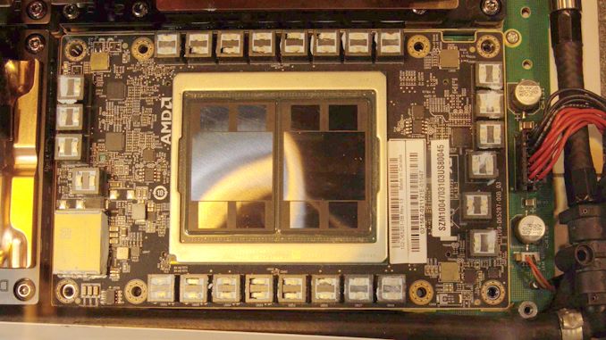
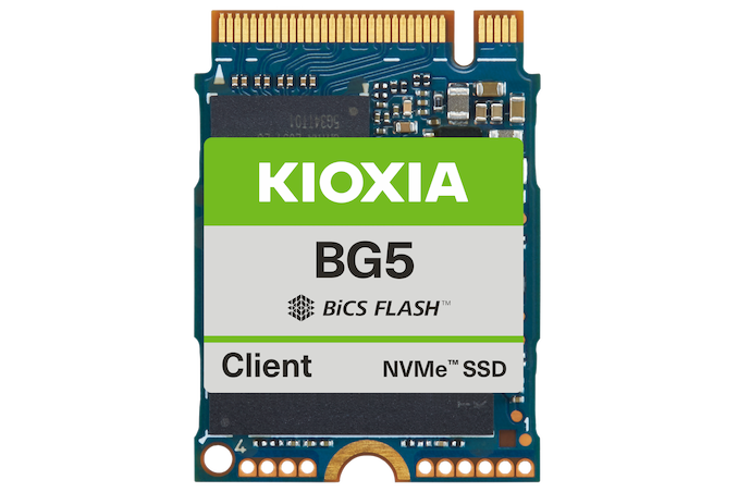
But perhaps the biggest change with the BG5 isn’t the specifications of the controller or the NAND on their own, but rather the fact that the two parts are alone to begin with. A staple of the BG5 series design has been the small package enabled by stacking the memory and controller together into a single package. But from Kioxia’s supplied product photo, we can clearly see that the NAND and the controller are separate packages. Kioxia made no mention of this change, so we can only speculate about whether it’s for simplicity in construction (no TSVs to the controller) or maybe the heat put off by a PCIe 4.0 controller. But one way or another, it’s a big change in how the small drive is assembled.


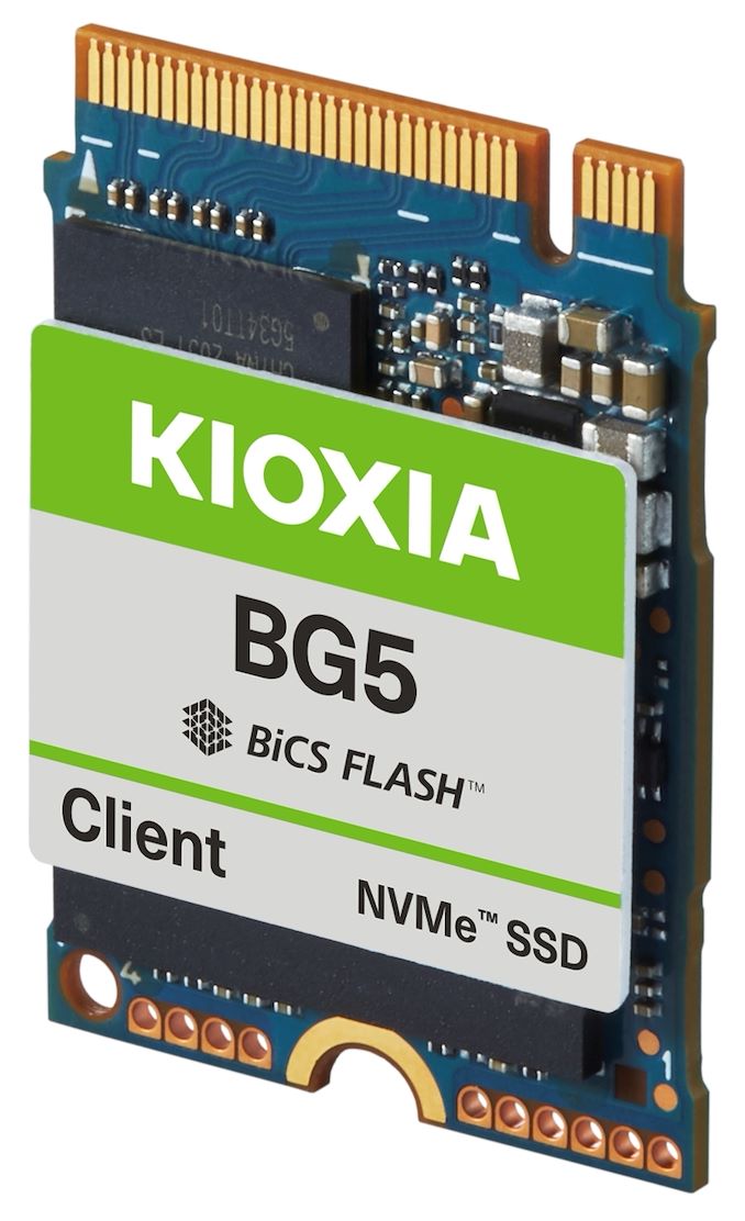
As a result of this change, the BGA M.2 1620 form factor – which supplied the single-chip package in a solder-down package – has gone away. Instead, the smallest form factor is now the removable M.2 2230 version. The postage stamp-sized M.2 2230 form factor has long been the staple of the lineup, as it’s what we’ve seen in Microsoft’s Surface products and other thin and light designs over the years. Since the form factor here isn’t changing, the use of multiple packages shouldn’t alter things much for a lot of OEMs. And for OEMs that need physically larger drives for compatibility reasons, Kioxia is also formally offering a 2280 design as well. A simple two-chip solution on such a large PCB is unremarkable, but it would allow the BG5 to be easily inserted into systems that are designed to take (and typically use) 2280 drives.


As these are OEM drives, no pricing information is available. The drives are currently sampling to Kioxia’s customers, so expect to see them land in commercial products in 2022.


Source: AnandTech – Kioxia Updates M.2 2230 SSD Lineup With BG5 Series: Adding PCIe 4.0 and BiCS5 NAND

Intel: Sapphire Rapids With 64 GB of HBM2e, Ponte Vecchio with 408 MB L2 Cache

This week we have the annual Supercomputing event where all the major High Performance Computing players are putting their cards on the table when it comes to hardware, installations, and design wins. As part of the event Intel is having a presentation on its hardware offerings, which discloses additional details about the next generation hardware going into the Aurora Exascale supercomputer.


Source: AnandTech – Intel: Sapphire Rapids With 64 GB of HBM2e, Ponte Vecchio with 408 MB L2 Cache

Cerebras Completes Series F Funding, Another $250M for $4B Valuation

Every once in a while, a startup comes along with something out of left field. In the AI hardware generation, Cerebras holds that title, with their Wafer Scale Engine. The second generation product, built on TSMC 7nm, is a full wafer packed to the brim with cores, memory, and performance. By using patented manufacturing and packaging techniques, a Cerebras CS-2 features a single chip, bigger than your head, with 2.6 trillion transistors. The cost for a CS-2, with appropriate cooling, power, and connectivity, is ‘a few million’ we are told, and Cerebras has customers that include research, oil and gas, pharmaceuticals, and defense – all after the unique proposition that a wafer scale AI engine provides. Today’s news is that Cerebras is still in full startup mode, finishing a Series F funding round.


Source: AnandTech – Cerebras Completes Series F Funding, Another 0M for B Valuation

Kingston XS2000 Portable SSDs Review: USB 3.2 Gen 2×2 Goes Mainstream

Flash-based portable drives have become popular fast storage options for both content creators and backups-seeking consumers. The advent of high-speed interfaces such as USB 3.2 Gen 2 (10 Gbps) and USB 3.2 Gen 2×2 (20 Gbps) along with Thunderbolt 3 (up to 40 Gbps) have enabled rapid improvements in performance of such portable SSDs over the last few years. While the higher-speed variants have traditionally been premium devices, a push towards lower priced drives was kickstarted by the introduction of native USB flash drive (UFD) controllers. Today, we are taking a look at the performance and value proposition of the complete Kingston XS2000 portable SSD lineup based on the Silicon Motion SM2320 controller.


Source: AnandTech – Kingston XS2000 Portable SSDs Review: USB 3.2 Gen 2×2 Goes Mainstream

The Intel Z690 Motherboard Overview (DDR5): Over 50+ New Models

To support the launch of Intel’s latest 12th generation ‘Alder Lake’ processors, Intel has also pulled the trigger on its latest Z690 motherboard chipset. Using a new LGA1700 socket, some of the most significant advancements with Alder Lake and Z690 include PCIe 5.0 support from the processor, as well as a PCIe 4.0 x8 link from the processor to the chipset. In this article, we’re taking a closer look at over 50+ different DDR5 enabled motherboards designed to not only use the processing power of Alder Lake but offer users a myriad of high-class and premium features.


Source: AnandTech – The Intel Z690 Motherboard Overview (DDR5): Over 50+ New Models

NVIDIA Launches A2 Accelerator: Entry-Level Ampere For Edge Inference

Alongside a slew of software-related announcements this morning from NVIDIA as part of their fall GTC, the company has also quietly announced a new server GPU product for the accelerator market: the NVIDIA A2. The new low-end member of the Ampere-based A-series accelerator family is designed for entry-level inference tasks, and thanks to its relatively small size and low power consumption, is also being aimed at edge computing scenarios as well.


Along with serving as the low-end entry point into NVIDIA’s GPU accelerator product stack, the A2 seems intended to largely replace what was the last remaining member of NVIDIA’s previous generation cards, the T4. Though a bit of a higher-end card, the T4 was designed for many of the same inference workloads, and came in the same HHHL single-slot form factor. So the release of the A2 finishes the Ampere-ficiation of NVIDIA accelerator lineup, giving NVIDIA’s server customers a fresh entry-level card.


NVIDIA ML Accelerator Specification Comparison
  A100 A30 A2
FP32 CUDA Cores 6912 3584 1280
Tensor Cores 432 224 40
Boost Clock 1.41GHz 1.44GHz 1.77GHz
Memory Clock 3.2Gbps HBM2e 2.4Gbps HBM2 12.5Gbps GDDR6
Memory Bus Width 5120-bit 3072-bit 128-bit
Memory Bandwidth 2.0TB/sec 933GB/sec 200GB/sec
VRAM 80GB 24GB 16GB
Single Precision 19.5 TFLOPS 10.3 TFLOPS 4.5 TFLOPS
Double Precision 9.7 TFLOPS 5.2 TFLOPS 0.14 TFLOPS
INT8 Tensor 624 TOPS 330 TOPS 36 TOPS
FP16 Tensor 312 TFLOPS 165 TFLOPS 18 TFLOPS
TF32 Tensor 156 TFLOPS 82 TFLOPS 9 TFLOPS
Interconnect NVLink 3

12 Links
PCIe 4.0 x16 +

NVLink 3 (4 Links)
PCIe 4.0 x8
GPU GA100 GA100 GA107
Transistor Count 54.2B 54.2B ?
TDP 400W 165W 40W-60W
Manufacturing Process TSMC 7N TSMC 7N Samsung 8nm
Form Factor SXM4 SXM4 HHHL-SS PCIe
Architecture Ampere Ampere Ampere


Going by NVIDIA’s official specifications, the A2 appears to be using a heavily cut-down version of their low-end GA107 GPU. With only 1280 CUDA cores (and 40 tensor cores), the A2 is only using about half of GA107’s capacity. But this is consistent with the size and power-optimized goal of the card. A2 only draws 60W out of the box, and can be configured to drop down even further, to 42W.


Compared to its compute cores, NVIDIA is keeping GA107’s full memory bus for the A2 card. The 128-bit memory bus is paired with 16GB of GDDR6, which is clocked at a slightly unusual 12.5Gbps. This works out to a flat 200GB/second of memory bandwidth, so it would seem someone really wanted to have a nice, round number there.


Otherwise, as previously mentioned, this is a PCIe card in a half height, half-length, single-slot (HHHL-SS) form factor. And like all of NVIDIA’s server cards, A2 is passively cooled, relying on airflow from the host chassis. Speaking of the host, GA107 only offers 8 PCIe lanes, so the card gets a PCIe 4.0 x8 connection back to its host CPU.


Wrapping things up, according to NVIDIA the A2 is available immediately. NVIDIA does not provide public pricing for its server cards, but the new accelerator should be available through NVIDIA’s regular OEM partners.


Source: AnandTech – NVIDIA Launches A2 Accelerator: Entry-Level Ampere For Edge Inference

Samsung Announces First LPDDR5X at 8.5Gbps

After the publication of the LPDDR5X memory standard earlier this summer, Samsung has now been the first vendor to announce new modules based on the new technology.


The LPDDR5X standard will start out at speeds of 8533Mbps, a 33% increase over current generation LPDDR5 based products which are running at 6400Mbps.


Source: AnandTech – Samsung Announces First LPDDR5X at 8.5Gbps

NVIDIA Announces Jetson AGX Orin: Modules and Dev Kits Coming In Q1’22

Today as part of NVIDIA’s fall GTC event, the company has announced that the Jetson embedded system kits will be getting a refresh with NVIDIA’s forthcoming Orin SoC. Due early next year, Orin is slated to become NVIDIA’s flagship SoC for automotive and edge computing applications. And, has become customary for NVIDIA, they are also going to be making Orin available to non-automotive customers through their Jetson embedded computing program, which makes the SoC available on a self-contained modular package.


Always a bit of a side project for NVIDIA, the Jetson single-board computers have none the less become an important tool for NVIDIA, serving as both an entry-point for helping bootstrap developers into the NVIDIA ecosystem, and as a embedded computing product in and of itself. Jetson boards are sold as complete single-board systems with an SoC, memory, storage, and the necessary I/O in pin form, allowing them to serve as commercial off the shelf (COTS) systems for use in finished products. Jetson modules are also used as the basis of NVIDIA’s Jetson developer kits, which throw in a breakout board, power supply, and other bits needed to fully interact with Jetson modules.


NVIDIA Jetson Module Specifications
  AGX Orin AGX Xavier Jetson Nano
CPU 12x Cortex-A78AE 8x Carmel

@ 2.26GHz
4x Cortex-A57

@ 1.43GHz
GPU Ampere Volta, 512 Cores

@ 1377MHz
Maxwell, 128 Cores

@ 920MHz
Accelerators Next-Gen NVDLA 2x NVDLA N/A
Memory 32GB LPDDR5, 256-bit bus

(204 GB/sec)
16GB LPDDR4X, 256-bit bus

(137 GB/sec)
4GB LPDDR4, 64-bit bus

(25.6 GB/sec)
Storage ? 32GB eMMC 16GB eMMC
AI Perf. (INT8) 200 TOPS 32 TOPS N/A
Dimensions 100mm x 87mm 100mm x 87mm 45mm x 70mm
TDP 15W-50W 30W 10W
Price ? $999 $129


With NVIDIA’s Orin SoC set to arrive early in 2022, NVIDIA is using this opportunity to announce the next generation of Jetson AGX products. Joining the Jetson AGX Xavier will be the aptly named Jetson AGX Orin, which integrates the Orin SoC.


Featuring 12 Arm Cortex-A78AE “Hercules” CPU cores and an integrated Ampere architecture GPU, and comprised of 17 billion transistors, Orin is slated to be a very powerful SoC once it begins shipping. The SoC also contains the latest generation of NVIDIA’s dedicated Deep Learning Accelerator (DLA), as well as a vision accelerator to further speed up and efficiently process those tasks.


Surprisingly, at this point NVIDIA is still holding back some of the specifications such as clockspeeds and the GPU configuration, so it’s not clear what the final performance figures will be like. But NVIDIA is promising 200 TOPS of performance in INT8 machine learning workloads, which would be a 6x improvement over AGX Xavier. Presumably those performance figures are for the module’s full 50W TDP, while performance is proportionally lower as you move towards the module’s minimum TDP of 15W.


For the AGX Jetson, Orin is being paired with 32GB of LPDDR5 RAM, which is attached to a 256-bit memory bus, allowing for 204GB/second of memory bandwidth. Unfortunately, NVIDIA is not listing how much storage the modules come with, though for reference, AGX Xavier came with 32GB of eMMC storage.


Meanwhile, for this generation NVIDIA will be maintaining pin and form-factor compatibility with Jetson AGX Xavier. So Jetson AGX Orin modules will be the same 100mm x 87mm in size, and use the same edge connector, making Orin modules drop-in compatible with Xavier.


Jetson AGX Oron modules and dev kits are slated to become available in Q1 of 2022. NVIDIA has not announced any pricing information at this time.


Source: AnandTech – NVIDIA Announces Jetson AGX Orin: Modules and Dev Kits Coming In Q1’22

AMD Confirms Milan-X with 768 MB L3 Cache: Coming in Q1 2022

As an industry, we are slowly moving into an era where how we package the small pieces of silicon together is just as important as the silicon itself. New ways to connect all the silicon include side by side, on top of each other, and all sorts of fancy connections that help keep the benefits of chiplet designs but also taking advantage of them. Today, AMD is showcasing its next packaging uplift: stacked L3 cache on its Zen 3 chiplets, bumping each chiplet from 32 MiB to 96 MiB, however this announcement is targeting its large EPYC enterprise processors.


Source: AnandTech – AMD Confirms Milan-X with 768 MB L3 Cache: Coming in Q1 2022

AMD Gives Details on EPYC Zen4: Genoa and Bergamo, up to 96 and 128 Cores

Since AMD’s relaunch into high-performance x86 processor design, one of the fundamental targets for the company was to be a competitive force in the data center. By having a competitive product that customers could trust, the goal has always been to target what the customer wants, and subsequently grow market share and revenue. Since the launch of 3rd Generation EPYC, AMD is growing its enterprise revenue at a good pace, however questions always turn around to what the roadmap might hold. In the past, AMD has disclosed that its 4th Generation EPYC, known as Genoa, would be coming in 2022 with Zen 4 cores built on TSMC 5nm. Today, AMD is expanding the Zen 4 family with another segment of cloud-optimized processors called Bergamo.


Source: AnandTech – AMD Gives Details on EPYC Zen4: Genoa and Bergamo, up to 96 and 128 Cores

AMD Announces Instinct MI200 Accelerator Family: Taking Servers to Exascale and Beyond

AMD today is formally unveiling their AMD Instinct MI200 family of server accelerators. Based on AMD’s new CDNA 2 architecture, the MI200 family is the capstone AMD’s server GPU plans for the last half-decade. By combing their GPU architectural experience with the latest manufacturing technology from TSMC and home-grown technologies such as their chip-to-chip Infinity Fabric, AMD has put together their most potent server GPUs yet. And with MI200 parts already shipping to the US Department of Energy as part of the Frontier exascale supercomputer contract, AMD is hoping that success will open up new avenues into the server market for the company.


Source: AnandTech – AMD Announces Instinct MI200 Accelerator Family: Taking Servers to Exascale and Beyond