Intel Sells SSD Business to SK hynix as new Subsidiary Solidigm

In a brief news release from Intel this afternoon, the chip firm has announced that it has closed on the first stage of its deal to sell its SSD business to SK hynix. As of today, SK hynix has now formally acquired the bulk of Intel’s NAND and SSD businesses, as well as the company’s NAND fab in Dalian, China. Intel will continue to hold a small stake until 2025, and in the meantime Intel’s former SSD assets have been spun-off into a new SK hynix subsidiary, Solidigm.


The Intel-SK hynix deal was first announced in October of 2020, with the two companies inking a deal to transfer over Intel’s NAND and SSD operations over to SK hynix over a several year timeframe. The deal, valued at $9 billion, would see Intel retain all of their Optane/3D XPoint technology and patents, while SK Hynix would receive all of Intel’s NAND-related business, including the Dalian NAND fab and Intel’s SSD business interests.


Now, with approval of the deal from all of the necessary regulatory bodies, the two companies have been able to close on the first part of the deal. The “first closing,” as Intel puts it, has transferred the Dalian fab as well as part of Intel’s SSD IP portfolio to SK hynix. Some employees are also being transferred – essentially all those who aren’t working for the fab or are involved in R&D. In return, SK hynix has paid Intel the first $7 billion of the deal.


The rest of the deal is set to close in three and a half years from now, in or around March of 2025. From now until then, Intel will continue to use the Dalian fab to manufacture NAND wafers. To do so, Intel has held on to some of their NAND-related IP, their R&D employees, and the fab employees. All of those assets will then finally be transferred to SK hynix once the deal fully closes and SK hynix pays Intel the final $2 billion.


Finally, SK hynix is taking the Intel assets they’ve acquired thus far and placing them into a new spin-off company, Solidigm. The standalone subsidiary, whose name is apparently a play on “paradigm” and “solid state storage” has setup shop in San Jose, and is being run by former Intel Non-Volatile Memory Solutions Group SVP and GM, Rob Crooke. Solidigm, in turn, has inherited Intel’s current NAND SSD product lineup; so Intel’s 660p and 670p client SSDs, as well as their D3/D5/D7 data center SSDs, are now in the process of becoming Solidigm products.


Source: AnandTech – Intel Sells SSD Business to SK hynix as new Subsidiary Solidigm

AMD and GlobalFoundries Wafer Supply Agreement Updated Once More: Now $2.1B Through 2025

In a short note published by AMD this afternoon as part of an 8-K filing with the US Securities and Exchange Commission, AMD is disclosing that the company has once again updated its wafer supply agreement with long-time fab partner (and AMD fab spin-off) GlobalFoundries. Under the terms of the latest wafer supply agreement, AMD and GlobalFoundries are now committing to buying and supplying respectively $2.1 billion in wafers for the 2022 through 2025 period, adding an additional year and $500M in wafers to the previous agreement.


As a quick refresher, AMD and GlobalFoundries last inked a new wafer supply agreement (WSA) back in May of this year. That agreement further decoupled the two firms, ending any exclusivity agreements between the two and allowing AMD to use any fab for any node as they see fit. None the less, AMD opted to continue buying 12nm/14nm wafers from GlobalFoundries, with the two firms inking a $1.6 billion agreement to buy wafers for the 2022 through 2024 period.


Officially classified as the First Amendment to the Amended and Restated Seventh Amendment to the Wafer Supply Agreement, the latest amendment is essentially adding another year’s worth of production to the WSA. The updated amendment now goes through 2025, with AMD raising their 12nm/14nm wafer orders by $500 million to $2.1 billion. AMD and GlobalFoundries are not disclosing the specific per-year wafer supply targets, but the agreement essentially binds GlobalFoundries to supply AMD will a bit over $500M in wafers every year for the next 4 years.


Along with yearly spending commitments, the updated agreement also updates the price of said wafers, as well as the pre-payment requirements for 2022/2023. As with the specific number of wafers, AMD isn’t disclosing any further details here.


AMD/GlobalFoundries Wafer Share Agreement History
Amendment Date December 2021 May 2021 January 2019
Total Order Value $2.1B $1.6B N/A
Start Date 2022 2022 2019
End Date 2025 2024 2024
GlobalFoundries Exclusivity? No No Partial

(12nm and larger)


It’s also worth noting that, as with the previous agreement, these targets are binding in both directions. GlobalFoundries is required to allocate a minimum amount of its capacity to orders from AMD, and AMD in turn is required to pay for these wafers, whether they use this capacity or not. Given the ongoing chip crunch, it would seem that AMD is hedging their bets here, and locking in some additional supply a couple of years in advance. Though given the price re-negotiation, it would be interesting to see if AMD had to agree to higher overall prices in order to secure a larger supply of wafers from GlobalFoundries.


Past that, AMD isn’t currently disclosing what they’ll be using the additional wafer capacity for – though they did clarify that it has nothing to do with acquisition target Xilinx. AMD currently uses GlobalFoundries’ 12nm/14nm processes for early-generation Ryzen products as well as the I/O dies for AMD’s current-generation Ryzen and EPYC CPUs. However under normal circumstances, we would expect demand for those products to be tapering off, especially by the 2024/2025 timeframe. The 12nm/14nm processes are already dated and are getting older still, so it’s unclear if this is AMD developing some backup plans to deal with the chip crunch, or if they are expecting demand for current 12/14 products to persist (e.g. if they need to produce their current long-term embedded products in larger numbers).


Baring any further amendments to the WSA, the current agreement between AMD and GlobalFoundries will now expire on December 31st, 2025.


On December 23, 2021, Advanced Micro Devices, Inc. (the “Company”) entered into the First Amendment (the “Amendment”) to its Amended and Restated Seventh Amendment to the Wafer Supply Agreement (the “A&R Seventh Amendment”) with GLOBALFOUNDRIES Inc. (“GF”) to extend GF’s capacity commitment and wafer pricing to the Company.


The Amendment modifies certain terms of the Wafer Supply Agreement applicable to wafer purchases at the 12 nm and 14 nm technology nodes by the Company for the period commencing on December 23, 2021 and continuing through December 31, 2025. GF agreed to increase the minimum annual capacity allocation to the Company for years 2022 through 2025. Further, the parties agreed to new pricing and annual wafer purchase targets for years 2022 through 2025, and modified the pre-payments agreed to by the Company to GF for those wafers in 2022 and 2023. The Amendment does not affect any of the prior exclusivity commitments that were removed under the A&R Seventh Amendment. The Company continues to have full flexibility to contract with any wafer foundry with respect to all products manufactured at any technology node. The Company currently estimates that it will purchase approximately $2.1 billion of wafers in total from GF for years 2022 through 2025 under the Amendment.


Source: AnandTech – AMD and GlobalFoundries Wafer Supply Agreement Updated Once More: Now .1B Through 2025

Intel Alder Lake DDR5 Memory Scaling Analysis With G.Skill Trident Z5

One of the most agonizing elements of Intel’s launch of its latest 12th generation Alder Lake desktop processors is its support of both DDR5 and DDR4 memory. Motherboards are either one or the other, while we wait for DDR5 to take hold in the market. While DDR4 memory isn’t new to us, DDR5 memory is, and as a result, we’ve been reporting on the release of DDR5 since last year. Now that DDR5 is here, albeit difficult to obtain, we know from our Core i9-12900K review that DDR5 performs better at baseline settings when compared to DDR4. To investigate the scalability of DDR5 on Alder Lake, we have used a premium kit of DDR5 memory from G.Skill, the Trident Z5 DDR5-6000. We test the G.Skill Trident Z5 kit from DDR5-4800 to DDR5-6400 at CL36 and DDR5-4800 with as tight timings as we could to see if latency also plays a role in enhancing the performance.


Source: AnandTech – Intel Alder Lake DDR5 Memory Scaling Analysis With G.Skill Trident Z5

Samsung Announces First PCIe 5.0 Enterprise SSD: PM1743, Coming In 2022

Even though CES 2022 is technically still a couple of weeks away, CES-related announcements are already starting to roll in. Among these are Samsung, who is announcing their first PCIe 5.0 SSD for servers, the PM1743. Based around a new, unnamed PCIe controller, Samsung’s latest server SSD is pairing that with the company’s current (sixth) generation V-NAND. Based on their published specifications, Samsung is touting upwards of 70-90% better performance over their previous-generation drive based on the workload. And tying in with CES in a couple of weeks, the new drive has already been awarded a CES 2022 Innovation Award.


At a high level, the PM1743 is the successor to Samsung’s current PM1733 enterprise SSD. Whereas the existing drive is based around a PCIe 4.0 controller and Samsung’s 96L fifth-generation V-NAND, the PM1743 bumps this up to PCIe 5.0 and 128L sixth-generation V-NAND instead. Given the general nature of today’s announcement, the company isn’t offering detailed technical specifications on the drive’s architecture, but between the NAND and controller improvements, they would seem to largely be able to keep up with the additional bandwidth afforded by the move to PCIe 5.0.


On paper, the PCie 5.0 x4 link the drive uses can reach bandwidth rates as high as 15.76GB/sec. For the PM1743, in turn, Samsung is claiming peak sequential read rates of 13GB/second, and peak sequential write rates of 6.6GB/sec (presumably to the drive’s SLC cache). This adds up to 86% higher peak read speeds and 89% higher peak write speeds than the PM1733. Or to put that in terms of IOPS, Samsung is claiming that the new drive will be able to hit 2.5M IOPS on random reads, and 250K IOPS on random writes.


Samsung Enterprise SSD Specifications
  PM1743

(15.36TB)
PM1733

(15.36TB)
Form Factor U.2 or E3.S U.2
Interface PCIe 5.0 x4, NVMe PCIe 4.0 x4, NVMe
Controller Unnamed Samsung PCIe 5.0 Samsung S4LR014 PCIe 4.0
NAND Flash Samsung 128L TLC? Samsing 96L TLC
Sequential Read 13000 MB/s 7000 MB/s
Sequential Write 6600 MB/s 3500 MB/s
Random Read

IOPS
2500k 1500k
Random Write

IOPS
250k 135k
Power Active 30 W? 20 W
Idle ? 8.5 W
Write Endurance ? 28 PBW

1.0 DWPD for 5 Years


The updated Samsung controller is also embedding its own security processor and root of trust. Samsung’s announcement is light on the details, but at a high level, the company is doubling down on security by giving the drive a degree of security control independent of the host server.


The company is also touting these updates as having improved the energy efficiency of the PM1743 by 30% over the PM1733, bringing it to 608MB/sec/watt. Given that data transfer rates have improved by upwards of 90% while power efficiency has only improved by 30%, it looks like the PM1743 will have a higher active power utilization rate than its predecessor. Doing some napkin math against the PM1733, which has a published figure of 20W, would put the active power of the PM1743 at around 30W.


Meanwhile, Samsung’s press release also confirms that the company has been working with Intel to validate the new drive. Samsung doesn’t go into any further details, but with Alder Lake (12th gen Core) already shipping now as the first mass market PCIe 5.0-capable platform, Samsung has presumably been testing against that, as well as the forthcoming Sapphire Rapids (next-gen Xeon) platform.


New for this generation of SSDs, Samsung will be offering the PM1743 in two form factors. The first will be the traditional 2.5-inch U.2 form factor. Meanwhile, joining U.2 will be E3.S, a newer 3-inch enterprise and data center form factor that is designed to be slightly larger than U.2 drives while incorporating a connector that can handle up to 16 lanes of PCIe.  SSDs of course won’t use that many lanes, but it’s a form factor that both drive and system vendors have been pushing for, making it the front-runner as the eventual successor to U.2. Based on last year’s publication of the E3 2.0 specification, we had been expecting E3.S drives to land in early 2022, so Samsung is right on time.


Finally, the PM1743 will be offered in capacities ranging from 1.92TB to 15.36TB, the same capacities the PM1733 is available at today. So although there is no capacity increase to speak of on a single drive level, since E3.S is half the thickness of a traditional 15mm U.2 drive, Samsung is touting the overall density improvements the new drive will afford. Essentially, if a server uses E3.S, it will be able to accommodate twice as many drives (and thus twice as much storage capacity) as a U.2 configuration.


The PM1743 is sampling now, and according to Samsung mass production will begin in the first quarter of next year.


Source: AnandTech – Samsung Announces First PCIe 5.0 Enterprise SSD: PM1743, Coming In 2022

Qualcomm’s 8cx Gen 3 for Notebooks, Nuvia Core in 2022/2023

There are many column inches detailing Qualcomm’s design wins and marketing strategy, however to paint it all with a broad brush, it has often boiled down to ‘where can we stick our advanced wireless technology?’. The company has had great success with smartphones, cornering a large chunk of US market and sizeable numbers worldwide, and in the last few years has pivoted to new markets, such as automotive and virtual reality, but also tried to reinvigorate existing markets, such as notebooks and laptops. Since 2017, Qualcomm has wedged a new category into the market, dubbed the ‘Always Connected PC’, offering Windows control with extreme battery life and mobile connectivity. At this year’s Tech Summit, Qualcomm introduced its latest processor, however the real magic might come next year.


Source: AnandTech – Qualcomm’s 8cx Gen 3 for Notebooks, Nuvia Core in 2022/2023

TSMC Unveils N4X Node: Extreme High-Performance at High Voltages

TSMC this week announced a new fabrication process that is tailored specifically for high-performance computing (HPC) products. N4X promises to combine transistor density and design rules of TSMC’s N5-family nodes with the ability to drive chips at extra high voltages for higher frequencies, which will be particularly useful for server CPUs and SoCs. Interestingly, TSMC’s N4X can potentially enable higher frequencies than even the company’s next-generation N3 process.


One of the problems that is caused by shrinking sizes of transistors is shrinking sizes of their contacts, which means increased contact resistance and consequent problems with power delivery. Various manufacturers use different ways of tackling the contact resistance issue: Intel uses cobalt contacts instead of tungsten contacts, whereas other makers opted to forming contacts using selective tungsten deposition technology. While these methods work perfectly for pretty much all kinds of chips, there are still ways to further improve power delivery for high-performance computing (HPC) designs, which are relatively immodest about the total about of power/voltage being used. This is exactly what TSMC did to its N4X node. But before we proceed to details about the new fabrication process, let us see what advantages TSMC promises with it. 


TSMC claims that its N4X node can enable up to 15% higher clocks compared to a similar circuit made using N5 as well as an up to 4% higher frequency compared to an IC produced using its N4P node while running at 1.2V. Furthermore – and seemingly more important – N4X can achieve drive voltages beyond 1.2V to get even higher clocks. To put the numbers into context: Apple’s M1 family SoCs made at N5 run at 3.20 GHz, but if these SoCs were produced using N4X, then using TSMC’s math they could theoretically be pushed to around 3.70 GHz or at an even higher frequency at voltages beyond 1.2V.


TSMC does not compare transistor density of N4X to other members of its N5 family, but normally processors and SoCs for HPC applications are not designed using high-density libraries. As for power, drive voltages of over 1.2V will naturally increase power consumption compared to chips produced using other N5-class nodes, but since the node is designed for HPC/datacenter applications, its focus is to provide the highest performance possible with power being a secondary concern. In fact, total power consumption has been increasing on HPC-class GPUs and similar parts for the last couple of generations now, and there is no sign this will stop in the next couple of generations of products, thanks in part to N4X.


“HPC is now TSMC’s fastest-growing business segment and we are proud to introduce N4X, the first in the ‘X’ lineage of our extreme performance semiconductor technologies,” said Dr. Kevin Zhang, senior vice president of Business Development at TSMC. “The demands of the HPC segment are unrelenting, and TSMC has not only tailored our ‘X’ semiconductor technologies to unleash ultimate performance but has also combined it with our 3DFabric advanced packaging technologies to offer the best HPC platform.”


Advertised PPA Improvements of New Process Technologies

Data announced during conference calls, events, press briefings and press releases
  TSMC
N5

vs

N7
N5P

vs

N5
N5HPC

vs

N5
N4

vs

N5
N4P

vs

N5
N4P

vs

N4
N4X

vs

N5
N4X

vs

N4P
N3

vs

N5
Power -30% -10% ? lower -22% ? ? -25-30%
Performance +15% +5% +7% higher +11% +6% +15%

or

more
+4%

or more
+10-15%
Logic Area


Reduction %


(Density)
0.55x


-45%


(1.8x)


0.94x


-6%


1.06x
0.94x


-6%


1.06x


?


?
0.58x


-42%


(1.7x)
Volume

Manufacturing
Q2 2020 2021 Q2 2022 2022 2023 H2 2022 H1

2024?
H1 2024? H2 2022


In a bid to increase performance and make drive voltages of over 1.2V possible, TSMC had to evolve the entire process stack.


  • First, it redesigned its FinFET transistors and optimized them both for high clocks and high drive currents, which probably means reducing resistance and parasitic capacitance and boosting the current flow through the channel. We do not know whether it had to increase gate-to-gate pitch spacing and at this point TSMC does not say what exactly it did and how it affected transistor density.
  • Secondly, it introduced new high-density metal-insulator-metal (MiM) capacitors for stable power delivery under extreme loads.
  • Thirdly, it redesigned back-end-of-line metal stack to deliver more power to transistors. Again, we do not know how this affected transistor density and ultimately die sizes.


To a large degree, Intel introduced similar enhancements to its 10nm Enhanced SuperFin (now called Intel 7) process technology, which is not surprising as these are natural methods of increasing frequency potential.


What is spectacular is how significantly TSMC managed to increase clock speed potential of its N5 technology over time. A 15% increase puts N4X close to its next-generation N3 fabrication technology. Meanwhile, with drive voltages beyond 1.2V, this node will actually enable higher clocks than N3, making it particularly good for datacenter CPUs.


TSMC says that expects the first N4X designs to enter risk production by the first half of 2023, which is a very vague description of timing, as it may mean very late 2022 or early 2023. In any case, it usually takes a year for a chip to proceed from risk production to high-volume production iteration, so it is reasonable to expect the first N4X designs to hit the market in early 2024. This is perhaps a weakness of N4X as by the time its N3 will be fully ramped and while N4X promises to have an edge in terms of clocks, N3 will have a major advantage in terms of transistor density.


Source: TSMC


Source: AnandTech – TSMC Unveils N4X Node: Extreme High-Performance at High Voltages

NVIDIA Announces GeForce RTX 2050, MX570, and MX550 For Laptops: 2022's Entry Level GeForce

NVIDIA this morning had made an unexpected news drop with the announcement of a trio of new GeForce laptop GPUs. Joining the GeForce family next year will be a new RTX 2000 series configuration, the GeForce RTX 2050, as well as an update to the MX lineup with the addition of the GeForce MX550 and GeForce MX570. The combination of parts effectively provide a refresh to the low-end/entry-level segment of NVIDIA’s laptop product stack, overhauling these products in time for new laptops to be released next year.


Source: AnandTech – NVIDIA Announces GeForce RTX 2050, MX570, and MX550 For Laptops: 2022’s Entry Level GeForce

Semi CapEx to Hit $152 Billion in 2021 as Market on Track for $2 Trillion by 2035

Semiconductor makers have drastically increased their capital expenditures (CapEx) this year in response to unprecedented demand for chips that is going to last for years. Now the CEO of Mubadala, the main stockholder of GlobalFoundries, is expecting sales of semiconductors to grow exponentially, toppling a whopping $2 trillion by mid-2030s. 


“It took 50 years for the semiconductor business to turn into a half a trillion-dollar business,” said Khaldoon Al Mubarak, CEO of Mubadala, in an interview with CNBC. “It is going to take probably eight to 10 years to double [by 2030 ~ 2031]. And it is going to double right after that, probably in four to five years.


Chipmakers are on track to spend $152 billion on new fabs and production equipment this year, up from $113.1 billion last year. On percentage basis, this is a 34% increase year-over-year, which is the strongest YoY growth since 2017 when cumulative CapEx of semiconductor companies increased by 41% per annum, IC Insights reports. 


Contract fabs like TSMC, Samsung Foundry, and GlobalFoundries will lead the whole industry in terms of CapEx spending, as they will pour in $53 billion in new fabs and equipment (35% of all semiconductor capital spending in 2021). 


TSMC, the world’s largest foundry, intended to spend between $25 billion and $35 billion on new manufacturing capacities as demand for its services is setting records. Furthermore, the company is preparing to ramp up production of chips using its N3 (3 nm) fabrication technology in 2023 and then N2 (2 nm) node in 2025, which requires buying new tools and building new fabs.


IC Insights expects TSMC to be the CapEx champion among all contract makers of chips this year followed by Samsung Foundry. By contrast, SMIC had to cut down its 2021 CapEx to $4.3 billion since it is extremely hard for a company in the U.S. Bureau of Industry and Security’s Entity List to procure tools from U.S.-based companies like Applied Materials, KLA, or Lam Research. GlobalFoundries also initiated expansion of production capacities in Germany, Singapore, and the U.S.


Meanwhile memory and flash manufacturers are expected to spend $51.9 billion on new fabs and production equipment this year. Since usage of NAND memory is increasing, spending on new flash production capacities is forecasted to reach $27.9 billion, whereas investments in DRAM production will total $24 billion. Interestingly, but CapEx on NAND will grow by 13% year-over-year, whereas expenditures on DRAM will increase by 34% YoY.


Microprocessor (MPUs) and microcontroller (MCUs) manufacturers, led by Intel, are on track to raise their CapEx to $23.5 billion this year, up 42% compared to 2020. IC Insights models sales of MPUs and MCUs in 2021 to hit $103.7 billion, up 14% from the previous year, and continue to grow at a compound annual growth rate (CAGR) of 7.1%through 2025, when their sales volume will reach $127.8 billion. Therefore, it is not surprising that companies are gearing up to meet demand for their chips in the coming years.


Intel alone expected to spend around $19 billion of CapEx money on expanding its factory network in 2021. While other suppliers of MPUs and MCUs have considerably lower CapEx budgets, they are also boosting their operations and are investing in things like dedicated packaging lines. 


Most applications that use processors or highly integrated controllers also tend to use different logic devices as well as analog and other components. To that end, suppliers of logic and analog/other devices are also increasing their CapEx spending by 40% and 41% year-over-year respectively as demand for their products is growing rapidly without any signs of slowing down.


Related Reading:


Source: AnandTech – Semi CapEx to Hit 2 Billion in 2021 as Market on Track for Trillion by 2035

Startup Showcases 7 bits-per-cell Flash Storage with 10 Year Retention

One of the key drivers to increase capacity in next generation storage has been to increase the number of bits that can be stored per cell. The easy jump of one to two bits-per-cell gives a straight 100% increase, in exchange for more control needed to read/write the bit but also limits the cell endurance. We’ve seen commercialization of storage up to four bits-per-cell, and talk about five. A Japanese company is now ready to start talking about their new 7 bits-per-cell solution.


Image courtesy of Plextor, up to 4 bits-per-cell


Moving from one to two bits-per-cell gives an easy doubling of capacity, and moving to three bits-per-cell is only another 50% increase. As more bits are added, the value of adding those bits diminishes, but the cost in the equipment to control the read and writes increases exponentially. There has to be a medium balance between how many bits-per-cell makes economic sense, and how much the control electronics costs to implement to enable those bits.


  • 1 bit per cell requires detection of 2 voltage levels, base capacity
  • 2 bit per cell requires detection of 4 voltage levels, +100% capacity
  • 3 bit per cell requires detection of 8 voltage levels, + 50% capacity
  • 4 bit per cell requires detection of 16 voltage levels, +33% capacity
  • 5 bit per cell requires detection of 32 voltage levels, +25% capacity
  • 6 bit per cell requires detection of 64 voltage levels, +20% capacity
  • 7 bit per cell requires detection of 128 voltage levels, +16.7% capacity


Also, the more bits-per-cell, the lower the endurance – the voltage variation when you store many bits only has to drift slightly to get the wrong result, and so repeated read/writes to a high capacity cell will make that voltage drift until the cell is unusable. Right now the market seems happy with three bits-per-cell (3bpc) for performance and four bits-per-cell (4bpc) for capacity, with a few 2bpc designs for longer term endurance. Some of the major vendors have been working on 5bpc storage, although the low endurance may make the technology only good for WORM – write once, read many, which is a common acronym for the equivalent of something like an old-school CD or non-rewritable DVD.


Floadia Corp., a Series C startup from Japan, issued a press release this week to state that it has developed st­­orage technology capable of seven bits-per-cell (7bpc). Still in the prototype stage, this 7bpc flash chip, likely in a WORM scenario, has an effective 10-year retention time for the data at 150C. The company says that a standard modern memory cell with this level of control would only be able to retail the data for around 100 seconds, and so the secret in the design is to do with a new type of flash cell they have developed.


The SONOS cell uses a distributed charge trap design relying on a Silicon-Oxide-Nitride-Oxide-Silicon layout, and the company points to an effective silicon nitride film in the middle where the charges are trapped to allow for high retention. In simple voltage program and erase cycles, the company showcases 100k+ cycles with a very low voltage drift. The oxide-nitride-oxide layers rely on SiO2 and Si3N4, the latter of which is claimed to be easy to manufacture. This allows a non-volatile SONOS cell to be used in NV-SRAM or embedded designs, such as microcontrollers.


It’s actually that last point which means we’re a long time from seeing this in modern NAND flash. Floadia is currently partnering with companies like Toshiba  to implement the SONOS cell in a variety of microcontrollers, rather than large NAND flash deployments, at the 40nm process node as embedded flash IP with compute-in-memory properties. Those aren’t at 7 bits-per-cell yet, to the effect that the company is promoting that two cells can store up to 8-bits of network weights for machine learning inference – when we get to 8 bits-per-cell, then it might be more applicable. The 10-year retention of the cell data is where it gets interesting, as embedded platforms will use algorithms with fixed weights over the lifetime of the product, except for the rare update perhaps. Even with increased longevity, Floadia doesn’t go into detail regarding cyclability at 7bpc at this time.


An increase from modern 3bpc to 6bpc NAND flash would afford a double density increase, however larger cells would be needed, which would negate the benefits. There’s also the performance aspect if the development of >4bpc ever made it to consumers, which hasn’t been touched upon.


It will be an interesting technology to follow.


Source: Floadia Press Release


Source: AnandTech – Startup Showcases 7 bits-per-cell Flash Storage with 10 Year Retention

SK Hynix to Manufacture 48 GiB and 96 GiB DDR5 Modules

Today SK Hynix is announcing the sampling of its next generation DDR5 memory. The headline is the commercialization of a new 24 gigabit die, offering 50% more capacity than the leading 16 gigabit dies currently used on high-capacity DDR5. Along with reportedly reducing power consumption by 25% by using SK Hynix’s latest 1a nm process node and EUV technology, what fascinates me most is that we’re going to get, for the first time in the PC space (to my knowledge), memory modules that are no longer powers of two.


For PC-based DDR memory, all the way back from DDR1 and prior, memory modules have been configured as a power of two in terms of storage. Whether that’s 16 MiB to 256 MiB to 2 GiB to 32 GiB, I’m fairly certain that all of the memory modules that I’ve ever handled have been powers of two. The new announcement from SK Hynix showcases that the new 24 gigabit dies will allow the company to build DDR5 modules in capacities of 48 GiB and 96 GiB.


To be clear, the DDR5 official specification actually allows for capacities that are not direct powers of two. If we look to other types of memory, powers of two have been thrown out the window for a while, such as in smartphones. However PCs and Servers, as least the traditional ones, have followed the power of two mantra. One of the changes in memory design that is now driving regular modules to non-power of two capacities is that it is getting harder and harder to scale DRAM capacities. The time it takes to figure out the complexity of the technology to get a 2x improvement every time is too long, and memory vendors will start taking those intermediate steps to get product to market.


In traditional fashion though, these chips and modules will be earmarked for server use first, for ECC and RDIMM designs. That’s the market that will absorb the early adopter cost of the hardware, and SK Hynix even says that the modules are expected to power high performance servers, particularly in machine learning as well as other HPC situations. One of the quotes on the SK Hynix press release was from Intel’s Data Center Group, so if there is any synergy related to support and deployment, that’s probably the place to start. A server CPU with 8x 64-bit channels and 2 DIMMs per channel gives 16 modules, and 16 x 48 GiB enables 768 GiB capacity.


As to when this technology will come to the consumer market, we’re going to have to be mindful of cost and assume that these chips will be used on high-cost hardware. So perhaps 48 GiB UDIMMs will be the first to market, although there’s a small possibility 24 GiB UDIMMs might make an appearance. Suddenly that 128 GiB limit on a modern gaming desktop will grow to 192 GiB.


Source: SKHynix Newsroom


Source: AnandTech – SK Hynix to Manufacture 48 GiB and 96 GiB DDR5 Modules

Seagate Introduces AMD EPYC-Based Exos Application Platform: Up To 1.344PB in 5U

Seagate’s Application Platform (AP) series of servers have targeted the market segments requiring tightly coupled storage and compute capabilities. The currently available SKUs – The Exos AP series with HDDs, and Nytro AP series with SSDs – are all based on Intel CPUs. That is changing today with the introduction of the Seagate Exos AP 5U84 based on the AMD EPYC Embedded 7292P processor.


The Exos AP 5U84 equipped with the 2nd Gen. AMD EPYC platform enables a high-density building block for private clouds and on-premises equipment, with 84 3.5″ HDD bays capable of storing up to 1.344PB (using Exos X16 HDDs) in a 5U form-factor. Capacity can further be expanded with EXOS E SAS expansion units. The platform includes redundancy options and all the other enterprise reliability functions expected in a storage / compute server. Networking with other rack components is enabled by dual port 25GbE controllers. The server processor can be configured for core counts of 8, 12, or 16 depending on required application compute requirements. The EPYC Embedded 7292P processor also include PCIe 4 lanes capable of delivering 200GbE network connectivity, if required.


Overall, the core count advantage and per-core power efficiency delivered by EPYC processors make it an ideal addition to Seagate’s AP series. Given AMD’s steady capturing of the server market, it doesn’t come as a surprise to see the AMD EPYC Embedded 7292P getting adopted in the storage market.


Source: AnandTech – Seagate Introduces AMD EPYC-Based Exos Application Platform: Up To 1.344PB in 5U

The Snapdragon 8 Gen 1 Performance Preview: Sizing Up Cortex-X2

At the recent Qualcomm Snapdragon Tech Summit, the company announced its new flagship smartphone processor, the Snapdragon 8 Gen 1. Replacing the Snapdragon 888, this new chip is set to be in a number of high performance flagship smartphones in 2022. The new chip is Qualcomm’s first to use Arm v9 as well as Samsung’s 4nm process node technology. In advance of devices coming in Q1, we attended a benchmarking session using Qualcomm’s reference design, and had a couple of hours to run tests focused on the new performance core, based on Arm’s X2 core IP.


Source: AnandTech – The Snapdragon 8 Gen 1 Performance Preview: Sizing Up Cortex-X2

Imagination Launches Catapult Family of RISC-V CPU Cores: Breaking Into Heterogeneous SoCs

December is here, and with it comes several technical summits ahead of the holiday break. The most notable of which this week is the annual RISC-V summit, which is being put on by the Linux Foundation and sees the numerous (and ever increasing) parties involved in the open source ISA gather to talk about the latest products and advancements in the RISC-V ecosystem.  The summit always tends to feature some new product announcements, and this year is no different, as Imagination Technologies is at the show to provide details on their first RISC-V CPU cores, along with announcing their intentions to develop a full suite of CPU cores over the next few years.


The company, currently best known for their PowerVR GPU lineup, has been dipping their toes into the RISC-V ecosystem for the last couple of years with projects like RVfpga. More recently, this past summer the company revealed in an earnings call that they would be designing RISC-V CPU cores, with more details to come. Now at the RISC-V summit they’re providing those details and more, with the formal announcement of their Catapult family of RISC-V cores, as well as outlining a heterogeneous computing-centric roadmap for future development.


Starting from the top, the Catapult family is Imagination’s overarching name for a complete family of RISC-V CPU cores, the first of which are launching today. Imagination has (and is) designing multiple microarchitectures in order to cover a broad range of performance/power/area (PPA) needs, and the Catapult family is slated to encompass everything from microcontroller-grade processors to high-performance application processors. All told, Imagination’s plans for the fully fleshed out Catapult family look a lot like Arm’s Cortex family, with Imagination preparing CPU core designs for microcontrollers (Cortex-M), real-time CPUs (Cortex-R), high performance application processors (Cortex-A), and functionally safe CPUs (Cortex-AE). Arm remains the player to beat in this space, so having a similar product structure should help Imagination smooth the transition for any clients that opt to disembark for Catapult.


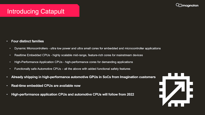
At present, Imagination has finished their first CPU core design, which is a simple, in-order core for 32-bit and 64-bit systems. The in-order Catapult core is being used for microcontrollers as well as real-time CPUs, and according to the company, Catapult microcontrollers are already shipping in silicon as part of automotive products. Meanwhile the real-time core is available to customers as well, though it’s not yet in any shipping silicon.


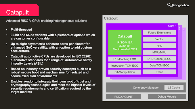
The current in-order core design supports up to 8 cores in a single cluster. The company didn’t quote any performance figures, though bear in mind this is a simple processor meant for microcontrollers and other very low power devices. Meanwhile, the core is available with ECC across both its L1 and TCM caches, as well as support for some of RISC-V’s brand-new extensions, such as the Vector computing extension, and potentially other extensions should customers ask for them.


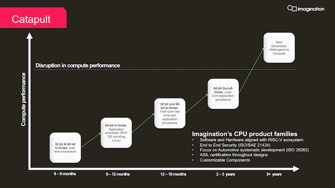
Following the current in-order core, Imagination has essentially three more core designs on their immediate roadmap. For 2022 the company is planning to release an enhanced version of the in-order core as an application processor-grade design, complete with support for “rich” OSes like Linux. And in 2023 that will be followed by another, even higher performing in-order core for the real-time and application processor markets. Finally, the company is also developing a much more complex out-of-order RISC-V core design as well, which is expected in the 2023-2024 timeframe. The out-of-order Catapult would essentially be their first take on delivering a high-performance RISC-V application processor, and like we currently see with high-performance cores the Arm space, has the potential to become the most visible member of the Catapult family.


Farther out still are the company’s plans for “next generation heterogeneous compute” designs. These would be CPU designs that go beyond current heterogeneous offerings – namely, just placing CPU, GPU, and NPU blocks within a single SoC – by more deeply combining these technologies. At this point Imagination isn’t saying much more, but they are making it clear that they aren’t just going to stop with a fast CPU core.


Overall, these are all clean room designs for Imagination. While the company has long since sold off its Meta and MIPS CPU divisions, it still retains a lot of the engineering talent from those efforts – along with ownership of or access to a large number of patents from the area. So although they aren’t reusing anything directly from earlier designs, they are hoping to leverage their previous experience to build better IP sooner.


Of course, CPU cores are just one part of what it will take to succeed in the IP space; besides incumbent Arm, there are also multiple other players in the RISC-V space, such as SiFive, who are all vying for much of the same market. So Imagination needs to both differentiate themselves from the competition, and offer some kind of market edge to customers.


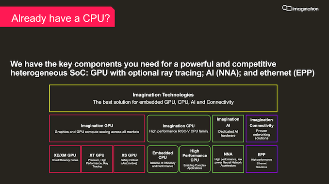
To that end, Imagination is going to be heavily promoting the possibilities for heterogenous computing designs with their IP. Compared to some of the other RISC-V CPU core vendors, Imagination already has well-established GPU and NPU IP, so customers looking to put together something more than just a straight CPU will be able to tap into Imagination’s larger library of IP. This does put the company more in direct competition with Arm (who already has all of these things as well), but then that very much seems to be Imagination’s goal here.


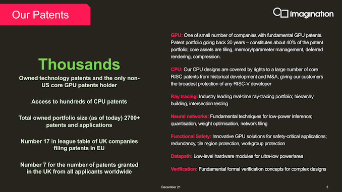
Otherwise, Imagination believes that their other big advantage in this space is the company’s history and location. As previously mentioned, Imagination holds access to a significant number of patents; so for clients who want to avoid extra patent licensing, they can take advantage of the fact that Imagination’s IP already comes indemnified against those patents. Meanwhile for chip designers who are based outside of the US and are weary of geopolitical issues affecting ongoing access to IP, Imagination is naturally positioned as an alternative there since they aren’t based in the US either – and thus access to their IP can’t be cut off by the US.


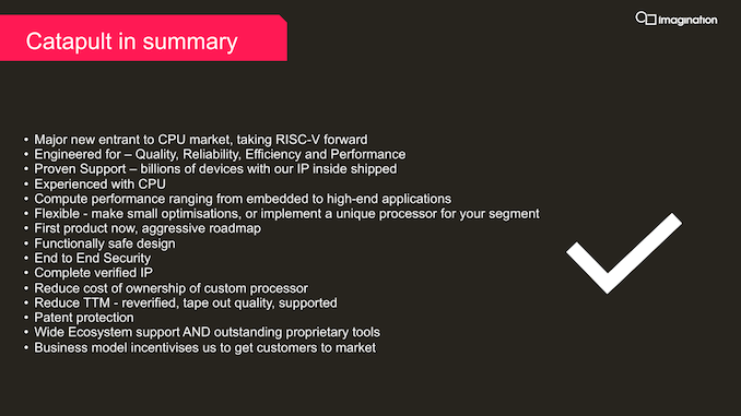
Wrapping things up, with the launch of their Catapult family of RISC-V CPU IP, imagination is laying out a fairly ambitious plan for the company for the next few years. By leveraging both their previous experience building CPUs as well as their current complementary IP like GPUs and NPUs, Imagination has their sights set on becoming a major player in the RISC-V IP space – and particularly when it comes to heterogeneous compute. Ultimately a lot will need to go right for the company before they can get there, but if they can succeed, then with their diverse collection of IP they would be in a rather unique position among RISC-V vendors.


Source: AnandTech – Imagination Launches Catapult Family of RISC-V CPU Cores: Breaking Into Heterogeneous SoCs

United States FTC Files Lawsuit to Block NVIDIA-Arm Acquisition

In the biggest roadblock yet to NVIDIA’s proposed acquisition of Arm, the United States Federal Trade Commission (FTC) has announced this afternoon that the regulatory body will be suing to block the merger. Citing concerns over the deal “stifling the innovation pipeline for next-generation technologies”, the FTC is moving to scuttle the $40 billion deal in order to protect the interests of the wider marketplace.


The deal with current Arm owner SoftBank was first announced in September of 2020, where at the time SoftBank had been shopping Arm around in an effort to either sell or spin-off the technology IP company. And while NVIDIA entered into the deal with bullish optimism about being able to close it without too much trouble, the company has since encountered greater political headwinds than expected due to the broad industry and regulatory discomfort with a single chip maker owning an IP supplier used by hundreds of other chip makers. The FTC, in turn, is the latest and most powerful regulatory body to move to investigate the deal – voting 4-0 to file the suit – following the European Union opening a probe into the merger earlier this fall. The


While the full FTC complaint has yet to be released, per a press release put out by the agency earlier today, the crux of the FTC’s concerns revolve around the advantage over other chip makers that NVIDIA would gain from owning Arm, and the potential for misconduct and other unfair acts against competitors that also rely on Arm’s IP. In particular, the FTC states that “Tomorrow’s technologies depend on preserving today’s competitive, cutting-edge chip markets. This proposed deal would distort Arm’s incentives in chip markets and allow the combined firm to unfairly undermine Nvidia’s rivals.”


To that end, the FTC’s complaint is primarily focusing on product categories where NVIDIA already sells their own Arm-based hardware. This includes Advanced Driver Assistance Systems (ADAS) for cars, Data Processing Units (DPUs) and SmartNICs, and, of course, Arm-based CPUs for servers. These are all areas where NVIDIA is an active competitor, and as the FTC believes, would provide incentive for NVIDIA to engage in unfair competition.


More interesting, perhaps, is the FTC’s final concern about the Arm acquisition: that the deal will give NVIDIA access to “competitively sensitive information of Arm’s licensees”, which NVIDIA could then abuse for their own gain. Since many of Arm’s customers/licensees are directly reliant on Arm’s core designs (as opposed to just licensing the architecture), they are also reliant on Arm to add features and make other alterations that they need for future generations of products. As a result, Arm’s customers regularly share what would be considered sensitive information with the company, which the FTC in turn believes could be abused by NVIDIA to harm rivals, such as by withholding the development of features that these rival-customers need.


NVIDIA, in turn, has announced that they will be fighting the FTC lawsuit, stating that “As we move into this next step in the FTC process, we will continue to work to demonstrate that this transaction will benefit the industry and promote competition.”


Ultimately, even if NVIDIA is successful in defending the acquisition and defeating the FTC’s lawsuit, today’s announcement means that the Arm acquisition has now been set back by at least several months. NVIDIA’s administrative trial is only scheduled to begin on August 9, 2022, almost half a year after NVIDIA initially expected the deal to close. And at this point, it’s unclear how long a trial would last – and how long it would take to render a verdict.


Source: AnandTech – United States FTC Files Lawsuit to Block NVIDIA-Arm Acquisition

Western Digital Spills Beans on HDD Plans: 30TB HDDs Planned, MAMR's Future Unclear

Western Digital this week said that its energy-assisted magnetic recording (ePMR) and OptiNAND technologies coupled with increased number of platters per hard drive would enable it to build HDDs with an up to 30 TB capacity. To keep advancing capacities from there, the company will need to use heat-assisted magnetic recording (HAMR), it revealed. Meanwhile, it never mentioned microwave-assisted magnetic recording (MAMR) that was expected to precede HAMR. 


Building a 22TB HDD for 2022


Last month Western Digital’s began shipping its top-of-the-range Ultrastar DC HC560 20TB and WD Gold 20TB hard drives that rely on nine 2.2 TB ePMR platters and feature the company’s OptiNAND technology that uses an embedded flash drive (EFD) to increase performance, reliability, and usable capacity of an HDD. 


To boost capacity of its next-generation hard drives further, Western Digital can either install disks with a higher areal density or increase the number of disks per drive. Both approaches have their challenges (higher areal density might require new heads, whereas an additional platter requires usage of thinner media and mechanical parts), but it looks like the company has a way to put 10th disk into a 3.5-inch HDD.


“We are able to deliver our 20TB on nine platters, we can add the 10th [disk], and we get another 2.2TB of storage,” said David Goeckeler, chief executive of Western Digital (via SeekingAlpha), at the 5th Annual Virtual Wells Fargo TMT Summit Conference.


Building a 22TB HDD on a 10-disk platform is a viable way to offer some additional capacity for its customers and stay competitive in 2022. But Western Digital’s existing technologies have a considerably more serious potential. 


Up to 30TB


When Western Digital introduced its OptiNAND technology earlier this year, it talked about its benefits (which include performance, reliability, and capacity) but did not really quantify them. This week the company finally spilled some beans on the potential of its ePMR technology combined with OptiNAND. As it turns out, it can build 30 TB hard drives using what it already has: ePMR, OptiNAND, and a 10-platter 3.5-inch HDD platform. This will require it to increase areal density of its ePMR disks by about 36%, which is significant.


“So, we really have that staircase to take you to 30TB and then you get on the HAMR curve and you go for quite a bit longer,” said Goeckler. “So, I think it is a really good roadmap for the hard drive industry.”


MAMR Axed?


For years Western Digital envisioned that its MAMR technology as a key enabler of its hard drives with an up to 40TB capacity. In 2019 it introduced its ePMR technology that was considered to be a half-way towards MAMR, but since then the company has barely mentioned MAMR at all.


When it announced its OptiNAND technology, Western Digital mentioned MAMR as one of the energy-assisted magnetic recording options it was looking at, but did not reveal any actual plans. At the virtual Wells Fargo summit, Western Digital stressed that HAMR was a key enabler for its future HDDs that have capacity of over 30TB, but did not talk about MAMR at all. 


“HAMR is extremely important, great technology, it is still several years away before it is commercialized, and you can bet your datacenter on it,” said Goeckler. “We have heavily invested in HAMR. I think you know we have over 400 patents in HAMR. [If] you are a supplier of hard drives in an industry this big, you are going to [invest] in a number of different technologies that you think is going to fuel your road map. So, we are a big believer in HAMR.”


If Western Digital can keep expanding capacity of its hard drives with its ePMR technology for a few years before it can roll out its first HAMR-based drives, then it does not need to commercialize its MAMR technology at all since HAMR has considerably better scalability in terms of aerial density. 


Like every new magnetic recording technology, MAMR and HAMR need to be evaluated by Western Digital’s customers before getting to mass production, which takes time. Therefore, it is not in the company’s interests to introduce new HDD platforms or new recording technologies too often as this slowdowns adoption of its drives by clients as well as revenue growth.


We have reached out to Western Digital to clarify its plans for MAMR, but the company has yet to respond to our request.


Source: AnandTech – Western Digital Spills Beans on HDD Plans: 30TB HDDs Planned, MAMR’s Future Unclear

Seagate Exos X20 and IronWolf Pro 20TB Expand Retail 20TB HDD Options

Seagate has updated their flagship capacity options for the retail HDD market with the availability announcement for two new hard drives today – the Exos X20 and IronWolf Pro 20TB. These two models join the recently-released Western Digital WD Gold 20TB and Ultrastar HC560 to round out the 20TB hard drives currently available for retail purchase.


The Exos X20 comes with SATA as well as SAS 12Gbps interface options, and includes SED (self-encrypting drive) models while the IronWolf Pro is SATA-only (similar to previous generations). The Exos X20 has a workload rating of 550 TB/yr, while the IronWolf Pro version is rated for 300 TB/yr. A detailed comparative summary of the different specifications of the two new drives and how they stack up against the Western Digital offerings is provided in the table below. Only the SATA options of the Exos X20 and the Ultrastar HC560 are being considered for this purpose. The two model numbers corresponding to these are for the SED and non-SED (standard) options.


2021 Retail 20TB HDDs – Comparative Specifications
  Seagate

Exos X20 20TB
Seagate

IronWolf Pro 20TB
Western Digital

WD Gold 20TB
Western Digital

Ultrastar HC560
Model ST20000NM007D

ST20000NM000D (SED)
ST20000NE000 WD201KRYZ WUH722020ALE6L1 (SED)

WUH722020ALE6L4
Recording Technology Conventional Magnetic Recording

(CMR)
Conventional Magnetic Recording with Energy-Assist

(CMR / EAMR)
RPM 7200 RPM
DRAM Cache 256 MB 512 MB
Helium-Filling Yes
Sequential Data Transfer Rate

(MBps)
285 MB/s 269 MB/s
MTBF 2.5 M 1.2 M 2.5 M
Rated Annual Workload 550 TB 300 TB 550 TB
Acoustics Idle 28 dB 20 dB
Seek 30 dB 32 dB 36 dB
Power Consumption Random read/write 9.4 W / 8.9 W (100R/100W @ QD16) 9.4 W / 8.9 W (100R/100W @ QD16) 7 W

(50R/50W @ QD1)
Idle 5.5 W 5.4 W 6 W
Warranty 5 Years 5 Years

(3 years DRS)
5 Years
Pricing $670 $650 $680 $700


The IronWolf Pro model also has a 1W standby / sleep-mode power consumption rating that could prove useful in NAS units that are subject to constant 24×7 traffic. The idle acoustics are at the higher end for the Seagate models, but the seek numbers make up for it. Unfortunately, we do not have a way to compare the power consumption numbers based on the datasheets, as the workloads used for the characterization are different between the two vendors. That said, the idle numbers lean again towards the Seagate models.


It must be noted here that the list price premium for the WD models can be accounted for by the use of OptiNAND technology in the WD Gold and Ultrastar HC560. We reached out to Seagate on the use of HAMR in the new models, and surprisingly, Seagate indicated that the two new hard drives being introduced to retail today do not use heat-assisted magnetic recording.


Source: AnandTech – Seagate Exos X20 and IronWolf Pro 20TB Expand Retail 20TB HDD Options

Qualcomm Announces Snapdragon 8 Gen 1: Flagship SoC for 2022 Devices

At this year’s Tech Summit from Hawaii, it’s time again for Qualcomm to unveil and detail the company’s most important launch of the year, and to showcase the newest Snapdragon flagship SoCs that will be powering our upcoming 2022 devices. Today, as the first of a few announcements at the event, Qualcomm is announcing the new Snapdragon 8 Gen 1, the direct follow-up to last year’s Snapdragon 888.


Source: AnandTech – Qualcomm Announces Snapdragon 8 Gen 1: Flagship SoC for 2022 Devices