Intel Goes Full XPU: Falcon Shores to Combine x86 and Xe For Supercomputers

One of Intel’s more interesting initiatives over the past few years has been XPU – the idea of using a variety of compute architectures in order to best meet the execution needs of a single workload. In practice, this has led to Intel developing everything from CPUs and GPUs to more specialty hardware like FPGAs and VPUs. All of this hardware, in turn, is overseen at the software level by Intel’s oneAPI software stack, which is designed to abstract away many of the hardware differences to allow easier multi-architecture development.


Intel has always indicated that their XPU initiative was just a beginning, and as part of today’s annual investor meeting, Intel is finally disclosing the next step in the evolution of the XPU concept with a new project codenamed Falcon Shores. Aimed at the supercomputing/HPC market, Falcon Shores is a new processor architecture that will combine x86 CPU and Xe GPU hardware into a single Xeon socket chip. And when it is released in 2024, Intel is expecting it to offer better than 5x the performance-per-watt and 5x the memory capacity of their current platforms.


At a very high level, Falcon Shores appears to be an HPC-grade APU/SoC/XPU for servers. While Intel is offering only the barest of details at this time, the company is being upfront in that they are combining x86 CPU and Xe GPU hardware into a single chip, with an eye on leveraging the synergy between the two. And, given the mention of advanced packaging technologies, it’s a safe bet that Intel has something more complex than a monolithic die planned, be it separate CPU/GPU tiles, HBM memory (e.g. Sapphire Rapids), or something else entirely.


Diving a bit deeper, while integrating discrete components often pays benefits over the long run, the nature of the announcement strongly indicates that there’s more to Intel’s plan here than just integrating a CPU and GPU into a single chip (something they already do today in consumer parts). Rather, the presentation from Raja Koduri, Intel’s SVP and GM of the Accelerated Computing Systems and Graphics (AXG) Group, makes it clear that Intel is looking to go after the market for HPC users with absolutely massive datasets – the kind that can’t easily fit into the relatively limited memory capacity of a discrete GPU.


A singular chip, in comparison, would be much better prepared to work from large pools of DDR memory without having to (relatively) slowly shuffle data in and out of VRAM, which remains a drawback of discrete GPUs today. In those cases, even with high speed interfaces like NVLink and AMD’s Infinity Fabric, the latency and bandwidth penalties of going between the CPU and GPU remain quite high compared to the speed at which HPC-class processors can actually manipulate data, so making that link as short as physically possible can potentially offer performance and energy savings.


Meanwhile, Intel is also touting Falcon Shores as offering a flexible ratio between x86 and Xe cores. The devil is in the details here, but at a high level it sounds like the company is looking at offering multiple SKUs with different numbers of cores – likely enabled by varying the number of x86 and Xe titles.


From a hardware perspective then, Intel seems to be planning to throw most of their next-generation technologies at Falcon Shores, which is fitting for its supercomputing target market. The chip is slated to be built on an “angstrom era process”, which given the 2024 date is likely Intel’s 20A process. And along with future x86/Xe cores, will also incorporate what Intel is calling “extreme bandwidth shared memory”.


With all of that tech underpinning Falcon Shores, Intel is currently projecting a 5x increase over their current-generation products in several metrics. This includes a 5x increase in performance-per-watt, a 5x increase in compute density for a single (Xeon) socket, a 5x increase in memory capacity, and a 5x increase in memory bandwidth. In short, the company has high expectations for the performance of Falcon Shores, which is fitting given the highly competitive HPC market it’s slated for.


And perhaps most interestingly of all, to get that performance Intel isn’t just tackling things from the raw hardware throughput side of matters. The Falcon Shores announcement also mentions that developers will have access to a “vastly simplified GPU programming model” for the chip, indicating that Intel isn’t just slapping some Xe cores into the chip and calling it a day. Just what this entails remains to be seen, but simplifying GPU programming remains a major goal in the GPU computing industry, especially for heterogeneous processors that combine CPU and GPU processing. Making it easier to program these high throughput chips not only makes them more accessible to developers, but reducing/eliminating synchronization and data preparation requirements can also go a long way towards improving performance.


Like everything else being announced as part of today’s investor meeting, this announcement is more of a teaser for Intel. So expect to hear a lot more about Falcon Shores over the next couple of years as Intel continues their work to bringing it to market.


Source: AnandTech – Intel Goes Full XPU: Falcon Shores to Combine x86 and Xe For Supercomputers

Intel’s Arctic Sound-M Server Accelerator To Land Mid-2022 With Hardware AV1 Encoding

Rounding out Intel’s direct GPU-related announcements from this morning as part of the company’s annual investor meeting, Intel has confirmed that the company is also getting ready to deliver a more traditional GPU-based accelerator card for server use a bit later this year. Dubbed Arctic Sound-M, the forthcoming accelerator is being aimed in particular at the media encoding and analytics market, with Intel planning to take full advantage of what should be the first server accelerator with hardware AV1 video encoding. Arctic Sound-M is expected to launch in the middle of this.


The announcement of Arctic Sound-M follows a hectic, and ultimately sidetracked set of plans for Intel’s original GPU server hardware. The company initially commissioned their Xe-HP series of GPUs to anchor the traditional server market, but Xe-HP was canceled in November of last year. Intel didn’t give up on the server market, but outside of the unique Ponte Vecchio design for the HPC market, they did back away from using quite so much dedicated server silicon.


In the place of those original products, which were codenamed Arctic Sound, Intel is instead coming to market with Arctic Sound-M. Given the investor-focused nature of today’s presentation, Intel is not publishing much in the way of technical details for their forthcoming server accelerator, but we can infer from their teaser videos that this is an Alchemist (Xe-HPC part), as we can clearly see the larger Alchemist die mounted on a single-slot card in Intel’s teaser video. This is consistent with the Xe-HP cancellation announcement, as at the time, Intel’s GPU frontman, Raja Koduri indicated that we’d see server products based on Xe-HPG instead.


Arctic Sound-M, in turn, is being positioned as a server accelerator card for the media market, with Intel calling it a “media and analytics supercomputer”. Accordingly, Intel is placing especially heavy emphasis on the media processing capabilities of the card, both in regards to total throughput and in codecs supported. In particular, Intel expects that Arctic Sound-M will be the first accelerator card released with hardware AV1 encoding support, giving the company an edge with bandwidth-sensitive customers who are ready to use the next-generation video codec.


Interestingly, this also implies that hardware AV1 encoding is a native feature of (at least) the large Alchemist die. Though given the potential value of the first hardware AV1 encoder, it remains to be seen whether Intel will enable it on their consumer Arc cards, or leave it restricted to their server card.


Meanwhile in terms of compute performance for media analytics/AI inference, Intel is quoting a figure of 150 TOPS for INT8. There aren’t a ton of great comparisons here in terms of competing hardware, but the closest comparison in terms of card size and use cases would be NVIDIA’s A2 accelerator, where on paper, the Arctic Sound-M would deliver almost 4x the inference performance. It goes without saying that the proof is in the pudding for a new product like Intel’s GPUs, but if they can deliver on these performance figures, then Arctic Sound-M would be able to safely occupy a very specific niche in the larger server accelerator marketplace.


Past that, like the rest of Intel’s Arc(tic) products, expect to hear more details a bit later this year.


Source: AnandTech – Intel’s Arctic Sound-M Server Accelerator To Land Mid-2022 With Hardware AV1 Encoding

Intel Meteor Lake Client Processors to use Arc Graphics Chiplets

Continuing with this morning’s spate of Intel news coming from Intel’s annual Investor meeting, we also have some new information on Intel’s forthcoming Meteor Lake processors, courtesy of this morning’s graphics presentation. Intel’s 2023 client processor platform, Meteor Lake was previously confirmed by the company to use a chiplet/tile approach. Now the company is offering a bit more detail on their tile approach, confirming that Meteor Lake will use a separate graphics tile, and offering the first visual mock-up of what this tiled approach will look like.


First revealed back in March of 2021, Meteor Lake is Intel’s client platform that will follow Raptor Lake – the latter of which is Alder Lake’s successor. In other words, we’re looking at Intel’s plans for their client platform two generations down the line. Among the handful of details revealed so far about Meteor Lake, we know that it will take a tiled approach, and that the compute tile will be built on the Intel 4 process, the company’s first EUV-based process.


Now, thanks to this morning’s investor presentation, we have our first look at the graphics side of Meteor Lake. For Intel’s 2023/2024 platform, Intel isn’t just offering a compute tile separate from an IO/SoC tile, but graphics will be their own tile as well. And that graphics tile, in turn, will be based on Intel’s Arc graphics technologies – presumably the Battlemage architecture.


In describing the significance of this change to Intel’s investor audience, GPU frontman Raja Koduri underscored that the tiled approach will enable Intel to offer performance more along the lines of traditional discrete GPUs while retaining the power efficiency of traditional integrated GPUs. More pragmatically, Battlemage should also be a significant step up from Intel’s existing Xe-LP integrated GPU architecture in terms of features, offering at least the full DirectX 12 Ultimate (FL 12_2) feature set in an integrated GPU. Per this schedule, this will put Intel roughly a year and a half to two years behind arch-rival AMD in terms of integrated graphics feature sets, as AMD’s brand-new Ryzen 6000 “Rembrandt” APUs are launching today with a DX12U-capable GPU architecture.


Past that, we’re expecting that Intel may have a bit more information on Meteor Lake this afternoon, as the company will deliver its client (Core) and server (Xeon) updates to investors as part of their live session later today. Of particular interest will be whether Intel embraces the tiled approach for the entire Meteor Lake family, or if they’ll hit a crossover point where they’ll want to produce a more traditional monolithic chip for the lower-end portion of the product stack. The Foveros technology being used to package Meteor Lake is cutting-edge technology, and cutting-edge tech often has cost drawbacks.


Source: AnandTech – Intel Meteor Lake Client Processors to use Arc Graphics Chiplets

Intel Arc Update: Alchemist Laptops Q1, Desktops Q2; 4mil GPUs Total for 2022

As part of Intel’s annual investor meeting taking place today, Raja Koduri, Intel’s SVP and GM of the Accelerated Computing Systems and Graphics (AXG) Group delivered an update to investors on the state of Intel’s GPU and accelerator group, including some fresh news on the state of Intel’s first generation of Arc graphics products. Among other things, the GPU frontman confirmed that while Intel will indeed ship the first Arc mobile products in the current quarter, desktop products will not come until Q2. Meanwhile, in the first disclosure of chip volumes, Intel is now projecting that they’ll ship 4mil+ Arc GPUs this year.


In terms of timing, today’s disclosure confirms some earlier suspicions that developed following Intel’s CES 2022 presentation: that the company would get its mobile Arc products out before their desktop products. Desktop products will now follow in the second quarter of this year, a couple of months behind the mobile parts. And finally, workstation products, which Intel has previously hinted at, are on their way and will land in Q3.


The pre-recorded presentation from Koduri does not offer any further details as to why Intel has their much-awaited Arc Alchemist architecture-based desktop products trailing their mobile products by a quarter. We know from previous announcements that the Alchemist family is comprised of two GPUs, so it may be that Intel is farther ahead on manufacturing and delivering the smaller of the two GPUs, which would be best suited for laptops. Alternatively, the company may be opting to focus on laptops first since it would allow them to start with OEM devices, and then expand into the more complex add-in board market a bit later. In any case, it’s a notable departure from the traditional top-to-bottom, desktop-then-laptop style launches that current GPU titans NVIDIA and AMD have favored. And this means that eager enthusiasts looking for an apples-to-apples look at how Intel’s first high-end GPU architecture fares, we’re going to be waiting a bit longer than initially expected.


Meanwhile, between mobile, desktop, and workstation products, Intel is expecting to ship over 4 million units/GPUs for 2022. To put this in some kind of reference, Jon Peddie Research estimates that the GPU AIB industry shipped 12.7 million boards in Q3’21. Which, pending Q4 numbers being released, would have put the industry as having shipped over 40 million discrete boards altogether over 2021. And while this is a bit of an apples-to-oranges comparison since Intel is counting both AIB desktop and mobile products, it does underscore the overall low volume of Alchemist chips that Intel is expecting to sell this year. Assuming AMD and NVIDIA deliver as many chips in 2022 as they did in 2021, Intel will be adding at most no more than another 10% to the overall volume of GPUs sold.


On the whole, this isn’t too surprising given both current manufacturing constraints and Intel’s newcomer status. The company is using TSMC’s N6 process to fab their Alchemist GPUs, and TSMC remains capacity constrained during the current chip crunch; so how many wafers Intel could hope to get was always going to be limited. Meanwhile as a relative newcomer to the discrete GPU space – a market that has been an NVIDIA/AMD duopoly for most of the past two decades – Intel doesn’t have the customer inertia that comes from offering decades of products. So even if Alchemist products perform very well relative to the competition, the company still needs time to grow into AMD and NVIDIA-sized shoes and to woo over the relatively conservative OEM base.


Celestial Architecture Under Development: Targeting Ultra Enthusiast Market


Along with the update on Alchemist, Koduri’s presentation also offered a very (very) brief update on Celestial, Intel’s third Arc architecture. Celestial is now under development, and at this point, Intel is expecting it to be their first product to address the ultra-enthusiast market (i.e. the performance crown). GPUs based on the Celestial architecture are expected in the “2024+” timeframe; which is to say that at this far out Intel doesn’t seem to know for sure if they’ll be 2024 or 2025 products.


Covering the gap between Alchemist and Celestial will be Battlemage, the second of Intel’s Arc GPU architectures. Battlemage now has a 2023-2024 release date, with Intel expecting the architecture to improve performance over Alchemist to the point where Battlemage will be competitive in the enthusiast GPU market – but not quite reaching the ultra-enthusiasts that Celestial will.


Finally, by virtue of this disclosure, it would seem that Battlemage will be the first Arc GPU architecture to make it into Intel’s CPUs. The company has it slated to be implemented as a tile on Meteor Lake CPUs, making this the crossover point where Intel’s current Xe-LP GPU architecture finally gets retired in favor of a newer GPU architecture.


Source: AnandTech – Intel Arc Update: Alchemist Laptops Q1, Desktops Q2; 4mil GPUs Total for 2022

Crucial Ballistix Memory Goes End-of-Life, Micron Realigns its DRAM Strategy

Underscoring the fast-paced nature of the computer hardware market, Micron this week has decided to discontinue all of its current Crucial Ballistix memory products. The move to end-of-life (EOL) these products covers the entire Ballistix lineup, such as the vanilla Ballistix, Ballistix MAX, and Ballistix MAX RGB series. Word of this change comes from a press announcement from Micron, Crucial’s parent company, and marks the impending end of the line for its popular consumer-focused line-up. 


Over the years, I have personally used many of Crucial’s Ballistix series memory for different builds, even back as far as the days of its DDR2-800 kits with bold and stylish gold heatsinks. The latest Ballistix series for DDR4 mixed things up with a whole host of different color schemes such as white, black, and even those adopting integrated RGB heat spreaders designed to offer users varying levels of customizability. It seems those days are now set to come to an end, as Micron has decided to call time on the popular series designed for enthusiasts and gamers.


Despite there being no officially stated reason from Micron for the decision to cut its popular and premier consumer-focused Ballistix series from its arsenal, the press release does state, “The company will intensify its focus on the development of Micron’s DDR5 client and server product roadmap, along with the expansion of the Crucial memory and storage product portfolio”.


It should be noted that Micron or Crucial never advertised or mentioned the Ballistix brand during the market’s transition from DDR4 to DDR5 memory. It seems that the decision wasn’t a spur-of-the-moment one and that Micron, which is one of the three main DRAM manufacturers globally along with SK Hynix and Samsung, is looking to turn its attention to satisfying the growing demand for its server hardware and client-based customers.


Finally, it should be noted that the memory discontinuation doesn’t affect Crucial’s consumer storage products, such as the Crucial P5 and P2 NMVe M.2 storage drives, or Crucial’s X8 and X6 portable SSDs. It looks as  Crucial will still keep its toes in the consumer sector for storage, at least for now. Still, the glory days of its Ballistix series will be no more, and users can expect to see the brand die out entirely as DDR4 memory is phased out of the desktop platforms in the coming years to come.


Micron To End-of-Life (EOL) Crucial Ballistix Product Lines


BOISE, Idaho; Feb. 16, 2022 – Micron released the following information about a change to its business strategy for Crucial memory.


  • The company will end-of-life (EOL) its Crucial Ballistix, Crucial Ballistix MAX and Crucial Ballistix MAX RGB product lines.
  • The company will intensify its focus on the development of Micron’s DDR5 client and server product roadmap, along with the expansion of the Crucial memory and storage product portfolio.
  • The company will continue to support the performance compute and gaming communities with its award-winning SSD products, such as the Crucial P5 Plus Gen4 PCIe NVMe SSD, Crucial P2 Gen 3 NVMe SSD, and the popular Crucial X6 and Crucial X8 portable SSDs.
  • Teresa Kelley, Vice President and General Manager, Micron Commercial Products Group: “We remain focused on growing our NVMe and Portable SSD product categories, which both offer storage solutions for PC and console gamers. Additionally, Crucial JEDEC standard DDR5 memory provides mainstream gamers with DDR5-enabled computers with better high-speed performance, data transfers and bandwidth than previously available with Crucial Ballistix memory.”


Source: PCPer


Related Reading


Source: AnandTech – Crucial Ballistix Memory Goes End-of-Life, Micron Realigns its DRAM Strategy

Ampere Goes Quantum: Get Your Qubits in the Cloud

When we talk about quantum computing, there is always the focus on what the ‘quantum’ part of the solution is. Alongside those qubits is often a set of control circuitry, and classical computing power to help make sense of what the quantum bit does – in this instance, classical computing is our typical day-to-day x86 or Arm or others with ones and zeros, rather than the wave functions of quantum computing. Of course, the drive for working quantum computers has been a tough slog, and to be honest, I’m not 100% convinced it’s going to happen, but that doesn’t mean that companies in the industry aren’t working together for a solution. In this instance, we recently spoke with a quantum computing company called Rigetti, who are working with Ampere Computing who make Arm-based cloud processors called Altra, who are planning to introduce a hybrid quantum/classical solution for the cloud in 2023.


Source: AnandTech – Ampere Goes Quantum: Get Your Qubits in the Cloud

A Visit to Intel’s D1X Fab: Next Generation EUV Process Nodes

On a recent trip to the US, I decided to spend some time criss-crossing the nation for a couple of industry events and spend some of the time visiting friends and peers. One of those stops was at Intel’s D1X Fab in Hillsboro, Oregon, one of the company’s leading edge facilities used for both production and development. It’s very rare to get time in a fab as a member of the press – in the ten years covering the industry, I’m lucky to say this was my second, which is usually two more than most. As you can imagine, everything had to be pre-planned and pre-approved, but Intel managed to fit me into their schedule.


Source: AnandTech – A Visit to Intel’s D1X Fab: Next Generation EUV Process Nodes

Intel to Acquire Tower Semiconductor for $5.4B To Expand IFS Capabilities

Continuing their recent spending spree in expanding their foundry capabilities, Intel this morning has announced that it has struck a deal to acquire specialty foundry Tower Semiconductor for $5.4 billion. If approved by shareholders and regulatory authorities, the deal would result in Intel significantly expanding its own contract foundry capabilities, acquiring not only Tower’s various fabs and specialty production lines, but also the company’s experience in operating contract foundries over the long run.


The proposed deal marks the latest venture from Intel that is designed to bolster Intel Foundry Services’ (IFS) production capabilities. In the last month and a half alone, Intel has announced plans to build a $20B fab complex in Ohio that will, in part, be used to fab chips for IFS, as well as a $1B fund to support companies building new and critical technologies for the overall foundry ecosystem. The Tower Semiconductor acquisition, in turn, is yet another piece of the puzzle for IFS, fleshing out Intel’s foundry capabilities for more exotic products.


As a specialty foundry, the Israel-based Tower Semiconductor is best known for its analog offerings, as well as its other specialized process lines. Among the chip types produced by Tower are MEMS, RF CMOS, BiCMOS, CMOS image sensors, silicon–germanium transistors, and power management chips. Essentially, Tower makes most of the exotic chip types that logic-focused Intel does not – so much so that Intel has been a Tower customer long before today’s deal was announced. All of which is why Intel wants the firm and its capabilities: to boost IFS’s ability to make chips for customers who aren’t after a straight ASIC processor.


The proposed acquisition would also see Intel pick up ownership of/access to the 8 foundry facilities that Tower uses. This includes the Tower-owned 150mm and 200mm fabs in Israel and two 200mm fabs in the US. Meanwhile Tower also has majority ownership in two 200mm fabs and a 300mm fab in Japan, and a future 300mm facility in Italy that will be shared with ST Microelectronics. As is typical for analog and other specialty processes where density is not a critical factor (if not a detriment), all of these fabs are based around mature process nodes, ranging from 1000nm down to 65nm, which sits in stark contrast to Intel’s leading-edge logic fabs.


Along with Tower’s manufacturing technology, the proposed deal would also see Intel pick up Tower’s expertise in the contract foundry business, which is something the historically insular Intel lacks. On top of their fab services, Tower also offers its customers electronic design automation and design services using a range of IP, all of which will be folded into IFS’s expanded offerings as part of the deal. Consequently, although the company has already brought on executives and other personnel with contract fab experience in past hirings, this would be the single largest talent transaction for IFS.


All told, Intel currently expects the deal to take around 12 months to close, with the company paying $5.4 billion in cash from its balance sheet for Tower Semiconductor shares. Though approved by both the Intel and Tower Semiconductor boards, Tower’s stockholders will still need to approve the deal. Intel will also need regulatory approval from multiple governments in order to close the deal, to which the company isn’t expecting much objection to given the complementary nature of the two companies’ foundry offerings. Still, as the last week alone has proven, regulatory approval for multi-billion dollar acquisitions is not always guaranteed.


Source: AnandTech – Intel to Acquire Tower Semiconductor for .4B To Expand IFS Capabilities

AnandTech Interview with Miguel Nunes: Senior Director for PCs, Qualcomm

During this time of supply crunch, there is more focus on ever on the PC and laptop markets – every little detail gets scrutinized depending on what models have what features and how these companies are still updating their portfolios every year despite all the high demand. One of the secondary players in the laptop space is Qualcomm, with their Windows on Snapdragon partnerships to bring Windows to Snapdragon powered laptops with x86 virtualization and a big bump in battery life as well as connectivity. The big crest on Qualcomm’s horizon in this space is the 2023 product lines, using CPU cores built by their acquisition of Nuvia. At Tech Summit in December 2021, we spoke to Qualcomm’s Miguel Nunes, VP and Senior Director of Product Management for Mobile Computing, who leads up the charge of the laptop division to see what’s coming down the pipe, and what measures Qualcomm are taking to bring a competitive product to market.


Source: AnandTech – AnandTech Interview with Miguel Nunes: Senior Director for PCs, Qualcomm

AMD’s Acquisition of Xilinx Receives Regulatory Go, Expected To Close Feb. 14th

Although it’s taken a bit longer than planned, AMD’s acquisition of Xilinx has finally cleared the last regulatory hurdles. With the expiration of the mandatory HSR waiting period in the United States, AMD and Xilinx now have all of the necessary regulatory approval to close the deal, and AMD expects to complete its roughly $53 billion acquisition of the FPGA maker on or around February 14th, 2 business days from now.


Having previously received approval from Chinese regulators late last month, the final step in AMD’s acquisition of Xilinx has been waiting out the mandatory Hart-Scott-Rodino (HSR) Act waiting period, which gives US regulators time to review the deal, and take more action if necessary. That waiting period ended yesterday, February 9th, with no action taken by the US, meaning that the US will not be moving to block the deal, and giving AMD and Xilinx the green light to close on it.


With all the necessary approvals acquired, AMD and Xilinx are now moving quickly to finally consummate the acquisition. AMD expects to complete that process in two more business days, putting the closure of the deal on (or around) February 14th – which is fittingly enough Valentine’s Day.


16 months in the making, AMD’s acquisition of Xilinx is the biggest acquisition ever for the Texas-based company. The all-stock transaction was valued at $35 billion at the time the deal was announced, offering 1.7234 shares of AMD stock for each Xilinx share. Since then, AMD’s stock price has increased by almost 51% to $125/share, which will put the final price tag on the deal at close to $53 billion – which is almost a third of AMD’s entire market capitalization and underscores the importance of this deal to AMD. Once the deal closes, Xilinx’s current stockholders will find themselves owning roughly 26% of AMD, while AMD’s existing stockholders hold the remaining 74%.


Having rebounded from their darkest days last decade, AMD has since shifted into looking at how to further grow the company, both by increasing its market share in its traditional products like CPUs and GPUs, as well as by expanding into new markets entirely. In particular, AMD has turned its eye towards expanding their presence in the data center market, which has seen strong and sustained growth for virtually everyone involved.


With AMD’s recent growth in the enterprise space with its Zen-based EPYC processor lines, a natural evolution one might conclude would be synergizing high-performance compute with adaptable logic under one roof, which is precisely the conclusion that Intel also came to several years ago. To that end, the high-performance FPGA markets, as well as SmartNICs, adaptive SoCs, and other controllable logic driven by FPGAs represent a promising avenue for future growth for AMD – and one they were willing to pay significantly for.


Overall, this marks the second major industry acquisition to be resolved this week. While NVIDIA’s takeover of Arm was shut down, AMD’s acquisition of Xilinx will close out the week on a happier ending. Ultimately, both deals underscore just how lucrative the market is for data center-class processors, and to what lengths chipmakers will go to secure a piece of that growing market.


Source: AnandTech – AMD’s Acquisition of Xilinx Receives Regulatory Go, Expected To Close Feb. 14th

Hands-On With The Huawei P50 Pro: The 2022 Flagship with a Snapdragon 888 Option

For those of us outside the US, Huawei has maintained its presence in a number of markets in which it has grown its sales over the last decade. Even without access to Google Services or TSMC, the company has been producing hardware and smartphones as it pivots to a new strategy. To lead off in 2022, that strategy starts with the Huawei P50 Pro, the next generation of flagship photography camera. The P series from Huawei has often been the lead device for new cameras and new features to attract creators, and the model we have today is a new twist in the Huawei story: our model comes with a Qualcomm flagship Snapdragon chip inside.


Source: AnandTech – Hands-On With The Huawei P50 Pro: The 2022 Flagship with a Snapdragon 888 Option

NVIDIA-Arm Acquisition Officially Nixed, SoftBank to IPO Arm Instead

NVIDIA’s year-and-a-half long effort to acquire Arm has come to an end this morning, as NVIDIA and Arm owner SoftBank have announced that the two companies are officially calling off the acquisition. Citing the current lack of regulatory approval of the deal and the multiple investigations that have been opened up into it, NVIDIA and SoftBank are giving up on their acquisition efforts, as the two firms no longer believe it will be possible to receive the necessary regulatory approvals needed to close the deal. In lieu of being able to sell Arm to NVIDIA (or seemingly anyone else), SoftBank is announcing that they will instead be taking Arm public.


First announced back in September of 2020, SoftBank and NVIDIA unveiled what was at the time a $40 billion deal to have NVIDIA acquire the widely popular IP firm. And though the two companies expected some regulatory headwind given the size of the deal and the importance of Arm’s IP to the broader technology ecosystem – Arm’s IP is in many chips in one form or another – SoftBank and NVIDIA still expected to eventually win regulatory approval.


However, after 17 months, it has become increasingly clear that government regulators were not apt to approve the deal. Even with concessions being made by NVIDIA, European Union regulators ended up opening an investigation into the acquisition, Chinese regulators have held off on approving the deal, and US regulators moved to outright block it. Concerns raised by regulators centered around NVIDIA gaining an unfair advantage over other companies who use Arm’s IP, both by controlling the direction of its development and by their position affording NVIDIA unique access to insights about what products Arm customers were developing – some of which would include products being designed to compete with NVIDIA’s own wares. Ultimately, regulators have shown a strong interest in retaining a competitive landscape for chips, with the belief that such a landscape wouldn’t be possible if Arm was owned by a chip designer such as NVIDIA.


As a result of these regulatory hurdles, NVIDIA and SoftBank have formally called off the acquisition, and the situation between the two companies is effectively returning to status quo. According to NVIDIA, the company will be retaining its 20 year Arm license, which will allow the company to continue developing and selling chips based around Arm IP and the Arm CPU architecture. Meanwhile SoftBank has received a $1.25 billion breakup fee from NVIDIA as a contractual consequence of the acquisition not going through.


In lieu of selling Arm to NVIDIA, SoftBank is now going to be preparing to take Arm public. According to the investment group, they are intending to IPO the company by the end of their next fiscal year, which ends on March 23rd of 2023 – essentially giving SoftBank a bit over a year to get the IPO organized. Meanwhile, according to Reuters, SoftBank’s CEO Masayoshi Son has indicated that the IPO will take place in the United States, most likely on the Nasdaq.


Once that IPO is completed, it will mark the second time that Arm has been a public company. Arm was a publicly-held company prior to the SoftBank acquisition in 2016, when SoftBank purchased the company for roughly $32 billion. And while it’s still too early to tell what Arm will be valued at a second time around, it goes without saying that SoftBank would like to turn a profit on the deal, which is why NVIDIA’s $40 billion offer was so enticing. Still, even with the popularity and ubiquity of Arm’s IP across the technology ecosystem, it’s not clear at this time whether SoftBank will be able to get something close to what they spent on Arm, in which case the investment firm is likely to end up taking a loss on the Arm acquisition.


Finally, the cancellation of the acquisition is also bringing some important changes to Arm itself. Simon Segars, Arm’s long-time CEO and major proponent of the acquisition, has stepped down from his position effective immediately. In his place, the Arm board of directors has already met and appointed Arm insider Rene Haas to the CEO position. Haas has been with Arm since 2013, and he has been president of the Arm IP Products Group since 2017.


Arm’s news release doesn’t offer any official insight into why Arm is changing CEOs at such a pivotal time. But with the collapse of the acquisition, Arm and SoftBank may be looking for a different kind of leader to take the company public over the next year.


Sources: NVIDIA, Arm


Source: AnandTech – NVIDIA-Arm Acquisition Officially Nixed, SoftBank to IPO Arm Instead

The Noctua NH-P1 Passive CPU Cooler Review: Silent Giant

In today’s review, we are having a look at a truly innovative cooler by Noctua, the NH-P1. The NH-P1 is a CPU cooler of colossal proportions, designed from the ground up with passive (fanless) operation in mind. Can a modern CPU operate seamlessly without a cooling fan? Noctua is here to prove that it can.


Source: AnandTech – The Noctua NH-P1 Passive CPU Cooler Review: Silent Giant

Western Digital Introduces WD_BLACK SN770: A DRAM-less PCIe 4.0 M.2 NVMe SSD

The initial wave of PCIe 4.0 NVMe SSDs put emphasis on raw benchmark numbers, with power consumption remaining an afterthought. The targeting of high-end desktop platforms ensured that it was not much of a concern. However, with the rise of notebook and mini-PC platforms supporting PCIe 4.0, power consumption and thermal performance became important aspects. With the gaming segment tending to be the most obvious beneficiary of PCIe 4.0 in the consumer market, speeds could also not be sacrificed much in this pursuit.


DRAM-less SSDs tend to be more power-efficient and also cost less, while delivering slightly worse performance numbers and consistency in general. There are multiple DRAM-less SSD controllers in the market such as the Phison E19T (used in the WD_BLACK SN750 SE and likely, the Micron 2450 series as well), Silicon Motion SM2267XT (used in the ADATA XPG GAMMIX S50 Lite), and the Innogrit IG5220 (used in the ADATA XPG ATOM 50). While performance tends to vary a bit with the NAND being used, the drives based on the Phison E19T and the Silicon Motion SM2267XT tend to top out around 3.9 GBps, while the Innogrit IG5220 reaches around 5 GBps.


Western Digital is throwing its hat into this ring today with the launch of the WD_BLACK SN770, powered by its own in-house DRAM-less SSD controller – the SanDisk 20-82-10081. It is wresting the performance crown in this segment with read speeds of up to 5150 MBps. A 20% improvement in power efficiency over the WD_BLACK SN750 SE is also being claimed by the company. The WD_BLACK SN770 will be available in four capacities ranging from 250GB to 2TB, with the complete specifications summarized in the table below.


Western Digital WD_BLACK SN770 SSD Specifications
Capacity 250 GB 500 GB 1 TB 2 TB
Model WDS250G3X0E WDS500G3X0E WDS100T3X0E WDS200T3X0E
Controller SanDisk 20-82-10081
NAND Flash BiCS 5 112L 3D TLC NAND?
Form-Factor, Interface Single-Sided M.2-2280, PCIe 4.0 x4, NVMe 1.4
DRAM N/A
Sequential Read 4000 MB/s 5000 MB/s 5150 MB/s
Sequential Write 2000 MB/s 4000 MB/s 4900 MB/s 4850 MB/s
Random Read IOPS 240K 460K 740K 650K
Random Write IOPS 470K 800K
Avg. Power Consumption ? W ? W ? W ? W
Max. Power Consumption ? W (R)

? W (W)
? W (R)

? W (W)
? W (R)

? W (W)
? W (R)

? W (W)
SLC Caching Yes
TCG Opal Encryption No
MTTF 1.75M Hours
Warranty 5 years
Write Endurance 200 TBW

0.44 DWPD
300 TBW

0.33 DWPD
600 TBW

0.33 DWPD
1200 TBW

0.33 DWPD
MSRP $59 (23.6¢/GB) $79 (15.8¢/GB) $129 (12.9¢/GB) $269 (13.45¢/GB)


The 1TB SKU appears to hit the sweet spot in terms of overall cost-efficiency as well as performance numbers. With the drive being part of the WD_BLACK lineup, the SSD is compatible with the WD_BLACK dashboard and its optional gaming mode (that turns off the low-power states to ensure the drive is operating in peak performance mode always). Thanks to the new controller, Western Digital’s own test results point to the SN770 outperforming the SN750 SE even with thermal throttling in the picture, with both drives tending to cool down on the performance front beyond 55C. The higher sequential read numbers help the SN770 to lower game loading times by as much as 40% compared to the SN750 SE – claims that we are hoping to put to test in the near future.


Overall, the pricing and the Western Digital brand name should contribute to the SN770 emerging as a compelling choice in the entry-level PCIe 4.0 NVMe SSD market. Despite the WD_BLACK branding, we believe the SSD has the key features to make it suitable even for notebook platforms which do not have gaming as the primary use-case.


Source: AnandTech – Western Digital Introduces WD_BLACK SN770: A DRAM-less PCIe 4.0 M.2 NVMe SSD

AMD Reports Q4 2021 and FY 2021 Earnings: Turning Silicon Into Gold

As the full year 2021 earnings season rolls along, the next major chip maker out of the gate is AMD, who has been enjoying a very positive trajectory in revenue and profits over the past few years. The company has continued to build upon the success of its Zen architecture-based CPUs and APUs in both the client and server spaces, as well as a full year’s revenue for the APUs powering the hard-to-find Playstation 5 and Xbox Series X|S. As a result, these products have propelled AMD to another record quarter and another record year, as the company continues to hit revenue records while recording some sizable profits in the process.


For the fourth quarter of 2021, AMD reported $4.8B in revenue, a 49% jump over the same quarter a year ago. As a result, Q4’2021 was (yet again) AMD’s best quarter ever, built on the back of strong sales across the entire company. Meanwhile, due to last year’s unusual, one-off gain related to an income tax valuation allowance, AMD’s GAAP net income did dip on a year-over-year basis, to $974M. In lieu of that, AMD’s quarterly non-GAAP net income (which excludes the tax allowance) was up 77% year-over-year, which is an even bigger jump than what we saw in Q4’20.


AMD’s continued growth and overall success has also boosted the company’s gross margin to 50%, marking the first time since at least the turn of the century that AMD has crossed the 50% mark. Besides underscoring the overall profitability of AMD’s operations, gross margins are also a good indicator of the health of a company; and for a fab-less semiconductor firm, 50% is a very good number to beat indeed. AMD is now within 5 percentage points of Intel’s gross margins, a feat that at one time seemed impossible, and highlighting AMD’s ascent to a top-tier chip firm.


AMD Q4 2021 Financial Results (GAAP)
  Q4’2021 Q4’2020 Q3’2021 Y/Y Q/Q
Revenue $4.8B $3.2B $4.3B +49% +12%
Gross Margin 50% 45% 48% +5.6pp +1.9pp
Operating Income $1.2B $570M $948M +112% +27%
Net Income $974M $1781M* $923M -45% +6%
Earnings Per Share $0.80 $1.45 $0.75 -45% +7%


As for AMD’s full-year earnings, the company has been having great quarters all year now, so unsurprisingly this is reflected in their full-year results. Overall, for 2021 AMD booked $16.4B in revenue, which was an increase of 68% over 2019, and, of course, sets a new record for the company. AMD’s gross margin for the year was 48%, up 3.7 percentage points from FY2020, and reflecting how AMD’s gross margins have been on the rise throughout the entire year.


All of this has played out nicely for AMD’s profitability, as well. For the year AMD booked $3.2 billion in net income, and unlike 2020, there are no one-off tax valuations inflating those numbers. Amusingly, even with that $1.3B valuation for 2020, AMD still beat their 2020 net income by a wide margin this year, bringing home $672M more. Or to look at things on a non-GAAP basis, net income was up 118% in a year, more than doubling 2020’s figures. Suffice it to say, the chip crunch has been very kind to AMD’s bottom line in the past year.


AMD FY 2021 Financial Results (GAAP)
  FY 2021 FY 2020 FY 2019 Y/Y
Revenue $16.4B $9.8B $6.7B +68%
Gross Margin 48% 45% 43% +3.7pp
Operating Income $3.6B $1369M $631M +166%
Net Income $3.2B $2490M* $341M +27%
Earnings Per Share $2.57 $2.06 $0.30 +25%


Moving on to individual reporting segments, 2021 was a year where all of AMD’s business units were seemingly firing on all cylinders. Client CPUs, GPUs, server CPUs, game consoles; 2021 will go down as the year where nobody could get enough of AMD’s silicon.


For Q4’21, AMD’s Computing and Graphics segment booked $2.6B in revenue, a 32% improvement over the year-ago quarter. According to the company, both Ryzen and Radeon sales have done very well here, with both product lines seeing further sales growth. On the CPU/APU front, average sale prices were up on both a yearly and quarterly basis, reflecting the fact that higher priced products are making up a larger share of AMD’s processor sales. And while AMD doesn’t offer a specific percentage breakdown, the company is reporting that notebook sales were once again the leading factor in AMD’s Ryzen revenue growth, coming on the back of strong demand for higher margin premium notebooks. And, based on overall growth in the number of processors sold, AMD believes that they’ve increased their market share (by revenue) for what would be the seventh straight quarter.


Meanwhile on the GPU front, AMD is reporting that graphics revenue has doubled on a year-over-year basis. According to the company, GPU ASPs are up on a year-over-year basis as well, though interestingly, they’re actually down on a quarterly basis due to what the company is attributing to the product mix – which in turn is presumably the ramp-up and launch of their first Navi 24-based products such as the RX 6500 XT. AMD’s prepared remarks don’t include any mentions of cryptocurrency, but it goes without saying that for the last year AMD has encountered little trouble in selling virtually every GPU it can get fabbed.


Finally, AMD also folds its data center/enterprise GPU sales under the C&G segment. There, AMD is reporting that revenue has more than doubled on a YoY basis, thanks to last year’s launch of the Instinct MI200 accelerator family. Unfortunately, AMD doesn’t offer any unit or revenue breakouts here to get a better idea of what data center shipments are like, or how much of those sales were MI250X accelerators for the Frontier supercomputer.


AMD Q4 2021 Reporting Segments
  Q4’2021 Q4’2020 Q3’2021

Computing and Graphics

Revenue $2584M $1960M $2398M
Operating Income $566M $420M $513M

Enterprise, Embedded and Semi-Custom

Revenue $2242M $1284M $1915M
Operating Income $762M $243M $542M


Meanwhile, AMD’s Enterprise, Embedded and Semi-Custom segment booked $2.2B in revenue for the quarter. The 75% year-over-year increase in revenue was driven by both improved EPYC sales as well as higher semi-custom sales.


As is usually the case, AMD doesn’t break apart EPYC and semi-custom sales figures, but the company is noting that data center, server, and cloud revenue – essentially everything EPYC except HPC – all more than doubled versus the year-ago quarter. All of which propelled AMD to doubling EPYC sales versus Q4’20, setting new records in the process. AMD has also noted that they’ve shipped their first V-cache enabled EPYC CPUs (Milan-X) to Microsoft, who is using them in an upcoming Azure instance type.


As for semi-custom sales, AMD is riding a wave of unprecedented demand for game consoles that has Sony and Microsoft taking every console APU they can get. Furthermore, despite this going on now for the last year and a half, AMD still expects semi-custom sales revenue to further grow in 2022 on the back of continued orders from console makers.


With all of that said, however, as AMD’s revenues have increased, so have their costs. For both the Client and Enterprise segments, the company is reporting that operating income growth has been partially offset by higher operating expenses. This encompasses both higher wafer prices from TSMC, as well as higher costs for things such as shipping. AMD can more than absorb the hit, of course, but it’s a reflection on how AMD has needed to spend more in order to secure wafers and supplies on an ongoing basis.


Looking forward, AMD is (understandably) once again expecting a very promising first quarter of 2022 and beyond. AMD has enjoyed significant revenue and market share growth over the past few years, and the company’s official forecasts are for that to continue into 2022. And, especially in the midst of the current and ongoing chip crunch, so long as demand holds, silicon may as well be gold for as valuable as it is to some of AMD’s customers.


To that end, AMD is officially projecting revenue growth of 31% for 2022, which would bring AMD to around $21.5B in sales. Given AMD’s 2021 estimate, this is likely once again conservative, though it is noteworthy in that it’s a bit less growth than AMD was projecting at this point a year ago for 2021. More interestingly, perhaps, is that AMD expects the non-GAAP gross margin for the year to land at around 51%, which even if it’s also a conservative estimate, would still be a big accomplishment for AMD.


Driving this growth will be a new slate of products for many of AMD’s important product lines. Along with ramping deliveries of Milan-X EPYC processors, AMD is also slated to deliver their Genoa EPYC processors, based on AMD’s Zen 4 CPU architecture, later this year. Zen 4 will also be making its appearance in Ryzen processors in H2’22, and in the meantime AMD has just launched their Zen3+ based Ryzen 6000 APUs for laptops. Finally, GPUs based on AMD’s forthcoming RDNA 3 architecture remain on the roadmap to be launched later this year as well.


Source: AnandTech – AMD Reports Q4 2021 and FY 2021 Earnings: Turning Silicon Into Gold

Interview with Alex Katouzian, Qualcomm SVP: Talking Snapdragon, Microsoft, Nuvia, and Discrete Graphics

Two driving forces are driving the current technology market: insatiable demand for hardware, and the supply chain shortages making it difficult to produce enough in quantity to fulfil every order. Even with these two forces in action, companies have to push and develop next generation technologies, as no competitor wants to sit on their laurels. That includes Qualcomm, and as part of the Tech Summit in late 2021, I sat down with Alex Katouzian, Qualcomm’s GM of Mobile, Compute, and Infrastructure to talk about the issues faced in 2021, the outlook for 2022, where the relationships lie, and where innovation is headed when it comes to smartphone and PC.


Source: AnandTech – Interview with Alex Katouzian, Qualcomm SVP: Talking Snapdragon, Microsoft, Nuvia, and Discrete Graphics

Intel Reports Q4 2021 and FY 2021 Earnings: Ending 2021 On A High Note

Kicking off yet another earnings season, we once again start with Intel. The reigning 800lb gorilla of the chipmaking world is reporting its Q4 2021 and full-year financial results, closing the book on an eventful 2021 for the company. The first full year of the pandemic has seen Intel once again set revenue records, making this the sixth record year in a row, but it’s also clear that headwinds are going to be approaching for the company, both in respect to shifts in product demand and in the sizable investments needed to build the next generation of leading-edge fabs.


Source: AnandTech – Intel Reports Q4 2021 and FY 2021 Earnings: Ending 2021 On A High Note

Launching This Week: NVIDIA's GeForce RTX 3050 – Ampere For Low-End Gaming

First announced as part of NVIDIA’s CES 2022 presentation, the company’s new GeForce RTX 3050 desktop video card is finally rolling out to retailers this month. The low-end video card is being positioned to round out the bottom of NVIDIA’s product stack, offering a modern, Ampere-based video card for a more entry-level market. All of this comes as PC video card market still in chaos due to a combination of the chip crunch and crypto miner demand, so any additional cards are most welcome – and likely to be sucked up rather quickly, even at a MSRP of $249 (and higher).


Source: AnandTech – Launching This Week: NVIDIA’s GeForce RTX 3050 – Ampere For Low-End Gaming

G.Skill Blitzes DDR5 World Record With Trident Z5 at DDR5-8888

For users buying a memory kit of DDR5, if they want to adhere to Intel specifications, will buy a DDR5-4800 kit. Though through XMP, there are other faster kits available – we’ve even tested G.Skill’s DDR5-6000 kit in our memory scaling article. But going above and beyond that, there’s overclocking.


Back in November 2021, extreme overclocker ‘Hocayu‘ managed to achieve DDR5-8704 using G.Skill’s Trident Z5 DDR5-6000 memory. As always with these records, they are made to be broken, and fellow Hong-Kong native lupin_no_musume has managed to surpass this with an impressive DDR5-8888, also using G.Skill Trident Z5 memory, with an ASUS’s ROG Maximus Z690 Apex motherboard, Intel’s Core i9-12900K processor, and some liquid nitrogen.


Without trying to sound controversial, indeed, extreme overclocking isn’t as popular as it once was. That isn’t to say it doesn’t have a purpose – using sub-ambient cooling methods such as liquid nitrogen, dry ice, and even liquid helium can boost frequencies on processors and graphics cards well beyond what’s achievable with standard cooling. Doing this not only shows the potential of hardware, but it also gives companies ‘bragging rights’ as being the proud owners of overclocking world records. Car companies boast about the best Nürburgring record for a variety of categories, or tuning their mainstream offerings, in a similar fashion.


G.Skill Trident Z5 DDR5-6000 (2 x 16 GB) memory kit. 


This not only pushes the boundaries of what DDR5 memory is capable of, but it’s also an impressive feat given DDR5 is relatively nascent. For reference, going from DDR5-6000 to DDR5-8888 represents an overclock of around 48% over the XMP profile and a crazy 85% overclock over the JEDEC specification of DDR5-4800. It should be worth noting that this is an all out data rate record regardless of latency, which in this case was increased to 88 over the standard 40, for stability. Going back to the car analogy, this would be akin to speed records on the drag strip, rather than on the oval.


Screenshot from G.Skill Trident Z5 DDR5-8888 CPU-Z validation (link)


While speeds of DDR5-8888 are not attainable in the form of purchasable memory kits for Alder Lake, G.Skill did unveil a retail kit that tops out at DDR5-7000. We also reported back in November 2021 that S.K. Hynix was planning for DDR5-8400 at 1.1 volts, but that’s actually part of the entended JEDEC specifications for when processors get verfied at that speed.


Source: G.Skill


Related Reading


Source: AnandTech – G.Skill Blitzes DDR5 World Record With Trident Z5 at DDR5-8888

Vulkan 1.3 Specification Released: Fighting Fragmentation with Profiles

Khronos this morning is taking the wraps off of Vulkan 1.3, the newest iteration of the group’s open and cross-platform API for graphics programming.


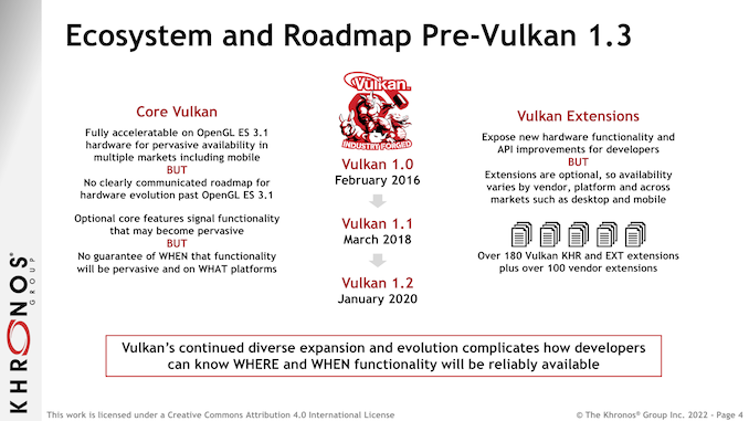
Vulkan 1.3 follows Khronos’s usual 2 year release cadence for the API, and it comes at a critical juncture for the API and its future development. Vulkan has been a full and official specification since 2016, turning 6 years old this year. This has given the API plenty of time to mature and have its kinks worked out, as well as to be adopted by software and hardware developers alike. But it also means that with the core aspects of the API having been hammered out, where to go next has become less obvious/harmonious. And with the API in use for everything from smartphones to high-end PCs, Vulkan is beginning to fragment at points thanks to the wide range of capabilities in devices.


As a result, for Vulkan 1.3, Khronos and its consortium members are taking aim at the future of the API, particularly from a development standpoint. Vulkan is still in a healthy place now, but in order to keep it that way, Khronos needs to ensure that Vulkan has room to grow with new features and functionality, but all without leaving behind a bunch of perfectly good hardware in the process. Thankfully, this isn’t a new problem for the consortium – it’s something virtually every standard faces if it lives long enough to become widely used – so Khronos is hitting the ground running with some further refinements to Vulkan.


Vulkan 1.3 Core


But before we get into Khronos’s fragmentation-fighting efforts, let’s first talk about what’s coming to the Vulkan 1.3 core specification. The core spec covers all of the features a Vulkan implementation is required to support, from the most basic smartphone to the most powerful workstation. As a result it has a somewhat narrow scope in terms of graphical features, but as the name says on the tin, it’s the common core of the API.


As with previous versions of the spec, Khronos is targeting this to work on existing Vulkan-compliant hardware. Specifically, Vulkan 1.3 is designed to work on OpenGL ES 3.1 hardware, meaning that of the new features being rolled into the core spec, none of them can be beyond what ES 3.1 hardware can do.


Consequently, Vulkan 1.3’s core spec isn’t focused on adding new graphical features or the like. By design, graphical feature additions are handled by extensions. Instead, the 1.3 core spec additions are largely a quality-of-life update for Vulkan developers, with a focus on adding features that simplify some aspect of the rendering process or add more control over it.


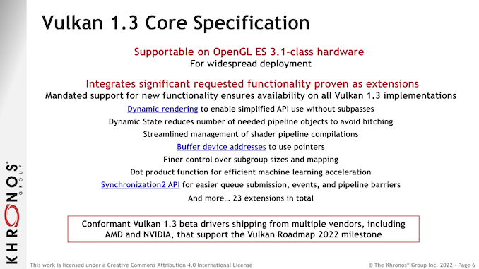
Altogether, Khronos is moving 23 existing extensions into the Vulkan 1.3 core spec. Most of these extensions are very much inside-baseball fodder for graphics programmers, but there are a couple of highlights. These include the integer dot product function, which is already widely used for machine learning inference on GPUs, as well as support for dynamic rendering. These functions already exist as extensions – so many developers can and are already using them – but by moving them into the core spec, they are now required for all Vulkan 1.3 implementations, opening them up to a wider array of developers.


But arguably the single most important addition coming to Vulkan isn’t an extension being promoted into the core specification. Rather, it’s entirely new functionality entirely, in the form of feature profiles.


Vulkan Profiles: Simplifying Feature Sets and Roadmaps


Up until now, Vulkan has not offered a concept of feature levels or other organizational grouping for additional feature sets. Beyond the core specification, everything in Vulkan is optional, all 280+ extensions. Meaning that for developers who are building applications that tap into features that go beyond the core spec – which has quickly become almost everything not written for a smartphone – there hasn’t been good guidance available on what extensions are supported on what platforms, or even what extensions are meant to go together.


The freedom to easily add extensions to Vulkan is one of the standard’s greatest strengths, but it’s also a liability if it’s not done in an organized fashion. And with the core spec essentially locked at the ES 3.1 level for the time being, this means that the number of possible and optional extensions has continued to bloom over the last 6 years.


So in an effort to bring order to the potential chaos, as well as to create a framework for planning future updates, Khronos is adding profiles to the Vulkan standard.


Profiles, in a nutshell, are a precisely defined lists of supported features and formats. Profiles don’t define any new API calls (that’s done by creating new extensions outright), so they are very simple conceptually. But, absent any kind of way to define feature sets, they are very important going forward for Vulkan.


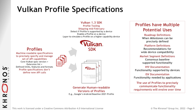
The power of profiles is that they allow for 280+ extensions to be organized into a much smaller number of overlapping profiles. Rather than needing to check to see if a specific PC video card supports a given extension, for example, a developer can just code against a (theoretical) “Modern Windows PC” profile, which in turn would contain all of the extensions commonly supported by current-generation PCs. Or alternatively, a mobile developer could stick to an Android-friendly profile, and quickly see what features they can use that will be supported by most devices.


At a high level, profiles are the solution to the widening gap between baseline ES 3.1 hardware, and what current and future hardware can do. Rather than risk fragmenting the Vulkan specification itself (and thus ending up with an OpenGL vs. OpenGL ES redux), profiles allow Vulkan to remain whole while giving various classes and generations of hardware their own common feature sets.


In line with the open and laissez faire nature of the Khronos consortium, profiles are not centrally controlled and can be defined by anyone, be it hardware devs, software devs, potato enthusiasts, or even Khronos itself. Similarly, whether a hardware/platform vendor wants to support a given profile is up to them; if they do, then they will need to make sure they expose the required extensions and formats. So this won’t be as neat and tidy as, say, Direct3D feature levels, but it will still be functional while offering the flexibility the sometimes loose consortium needs.


That said, Khronos’s expectation that we should only see a limited number of widely used profiles, many of which they’ll be involved with in some fashion. So 280 extensions should not become 280 profiles, at least as long as the hardware vendors can find some common ground across their respective platforms.


Finally, on a technical level, it’s worth noting that profiles aren’t just a loose list of features, but they do have technical requirements. Specifically, profiles are built as JSON lists, which along with providing a means to check profile compatibility, also open the door to things like generating human-readable versions of profiles. It’s a small distinction, but it will help developers quickly implement profile support in a generic fashion, relying on the specific JSON lists to guide their programs the rest of the way.


Profiles are also not limited to being built upon Vulkan 1.3. Despite being introduced at the same time as 1.3, they are actually a super-feature of sorts that can work with previous Vulkan versions, as all of the heavy lifting is being done at the application and SDK level. So it will be possible to have a profile that only calls for a Vulkan 1.0 implementation, for example.


Google’s Android Baseline 2021 Profile


The first profile out the door, in turn, comes from Google. The Android author is defining a Vulkan profile for their market that, at a high level, will help to better define and standardize what feature are available on most Android devices.


Interestingly, Google’s profile is built upon Vulkan 1.0, and not a newer version of Vulkan. From what we’re told, there are features in the Vulkan 1.1 core specification that are still not widely supported by mobile devices (even with the ES 3.1 hardware compatibility goal), and as a result, any kind of common progression with Vulkan on Android has become stalled. So since Google can’t get Vulkan 1.1/1.2/1.3 more widely supported across Android devices, the company is doing the next best thing and using a profile to define a bunch of common post-1.0 extensions that are supported by the current crop of devices.


The net result of this is the Android Baseline 2021 Profile. By establishing a baseline profile for the ecosystem, Google is aiming to not only make newer functionality more accessible to developers, but to simplify graphics programming in the process. Essentially, the Baseline 2021 Profile is a fix for existing fragmentation within the Android ecosystem by establishing a reasonable set of commonly supported features and formats.


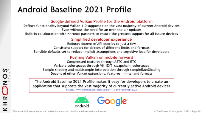
Of particular note, Google’s profile calls for support for both ETC and ASTC texture compression formats. As well, sample shading and multi-sample interpolation are on the list as well. Given that this is a baseline specification, there aren’t any high-concept next-generation features contained within the profile. But over time, that will change. Google has already indicated that they will be developing a 2022 profile for later this year, and will continue to keep adding further baseline profiles as the situation warrants.


Finally, Google’s use of profiles is also a solid example of taking advantage of the application-centric nature of profiles. According to Google, developers will be able to use profiles on the “vast majority” of Android devices without the need for over-the-air updates for those devices. Since profiles are handled at the application/SDK level, all the device itself needs to present are the necessary Vulkan extensions, which in accordance with a baseline specification are already present and supported in the bulk of Android devices.


Vulkan Roadmap 2022: Making Next-Generation Features Common Features


Last but certainly not least, the other big development to stem from the addition of profiles is a renewed path forward for developing and adopting new features for next-generation hardware. As mentioned previously, Vulkan has until now lacked a way to define feature sets for more advanced (non-core) features, which profiles are finally resolving. As a result, Khronos and the hardware vendors finally have the tools they need to establish baselines for not just low-end hardware, but high-end hardware as well.


In other words, profiles will provide the means to finally create some common standards that incorporate next-generation hardware and the latest programming features.


Because of Vulkan core’s ES 3.1 hardware requirements, there is a significant number of advanced features that have remained optional extensions. This includes everything from ray tracing and sample rate shading to more basic features like anisotropic filtering, multiple processor scheduling, and bindless resources (descriptor indexing). To be sure, these are all features that developers have had access to for years as extensions, but lacking profiles, there has been no assurance for developers that a given feature is going to be in all the platforms they want to target.


To that end, Khronos and its members have developed the Vulkan Roadmap 2022, which is both a roadmap of features they want to become common, as well as a matching profile to go with the roadmap. Conceptually, the Vulkan Roadmap 2022 feature set can be thought of as the inverse of Google’s baseline profile; instead of basing a profile around low-end devices, Roadmap 2022 excises low-end devices entirely in order to focus on common features found in newer hardware.


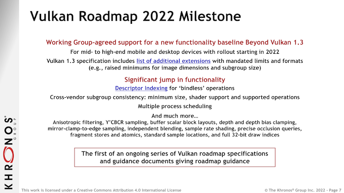
Roadmap 2022 is being based around features found in mid-end and high-end devices, mobile and PC alike. So while it significantly raises the bar in terms of features supported, it’s still not leaving mobile devices behind entirely – nor would it necessarily be ideal to do so. In practice, this means that Roadmap 2022 is slated to become the common Vulkan feature set for mid-end and better devices across the hardware spectrum.


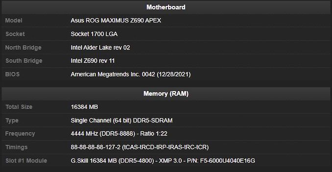
Meanwhile, adoption of Roadmap 2022 should come very quickly since it’s based around features and formats already supported in existing hardware. AMD and NVIDIA have already committed to enabling support for the necessary features in their Vulkan 1.3 drivers, which are out today in beta and should reach maturity in a couple of months. In fact, the biggest hold-up to using profiles is Khronos itself – the Vulkan SDK won’t get profile support until next month.


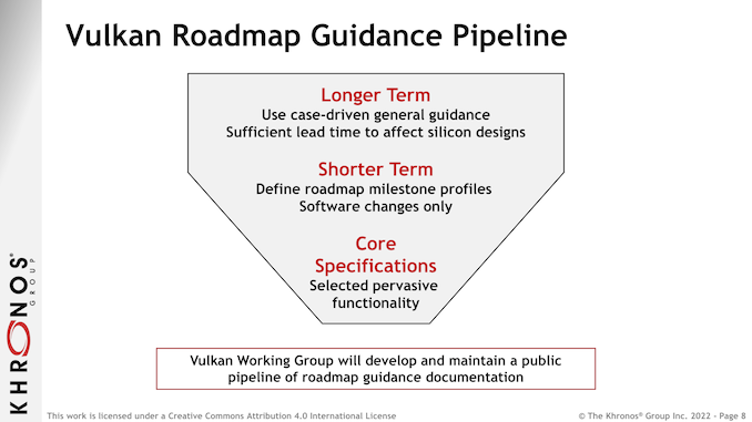
Finally, according to Khronos Roadmap 2022 is just the start of the roadmapping process for the group. After getting caught-up with current-generation hardware with this year’s profile, the group will be developing longer-term roadmaps for Vulkan profiles. Specifically, the group wants to get far enough ahead of the process that profiles are being planned out years in advance, when the next-generation of hardware is still under development. This would enable Khronos to have a compete pipeline of profiles in the works, giving hardware and software developers a roadmap for the next couple of years of Vulkan features.


Ultimately, having a roadmap will serve to help keep the development of advanced features for Vulkan on-track. Freed from having to support the oldest of hardware, the Vulkan group members will be able to focus on developing and implementing new features, knowing exactly when support is expected/planned/desired to arrive. Up until now the planning process has been weighed down by the lack of a timeline for making new features a requirement (de jure or otherwise), so having a formal process to standardize advanced features will go a long way towards speeding up and simplifying that process.


Source: AnandTech – Vulkan 1.3 Specification Released: Fighting Fragmentation with Profiles