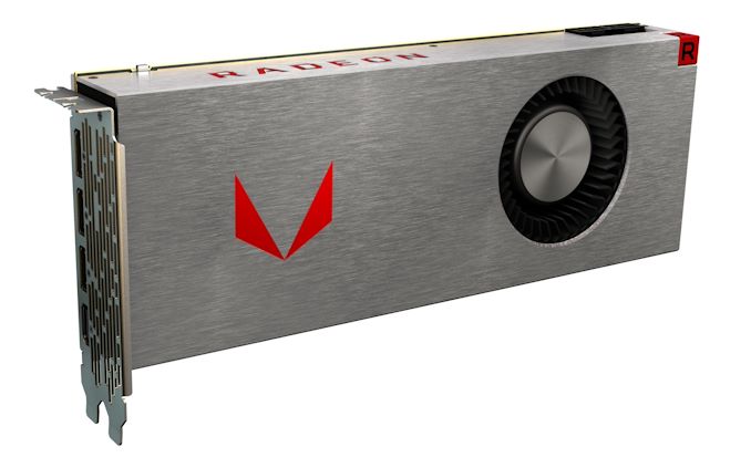
As AMD is now well into their third generation of RDNA architecture GPUs, the sun has been slowly setting on AMD’s remaining Graphics Core Next (GCN) designs, better known by the architecture names of Polaris and Vega. In recent weeks the company dropped support for those GPU architectures in their open source Vulkan Linux driver, AMDVLK, and now we have confirmation that the company is slowly winding down support for these architectures in their Windows drivers as well.
Under AMD’s extended driver support schedule for Polaris and Vega, the drivers for these architectures will no longer be kept at feature parity with the RDNA architectures. And while AMD will continue to support Polaris and Vega for some time to come, that support is being reduced to security updates and “functionality updates as available.”
For AMD users keeping a close eye on their driver releases, they’ll likely recognize that AMD already began this process back in September – though AMD hasn’t officially documented the change until now. As of AMD’s September Adrenaline 23.9 driver series, AMD split up the RDNA and GCN driver packages, and with that they have also split the driver branches between the two architectures. As a result, only RDNA cards are receiving new features and updates as part of AMD’s mainline driver branch (currently 23.20), while the GCN cards have been parked on a maintenance driver branch – 23.19.
At present, AMD has not published anything about this change in driver support to their website. But, responding to a request for a comment on Windows driver support from AnandTech, issued the following statement.
The AMD Polaris and Vega graphics architectures are mature, stable and performant and don’t benefit as much from regular software tuning. Going forward, AMD is providing critical updates for Polaris- and Vega-based products via a separate driver package, including important security and functionality updates as available. The committed support is greater than for products AMD categorizes as legacy, and gamers can still enjoy their favorite games on Polaris and Vega-based products.
Notably, AMD is actively asserting that this is not “legacy” status for Vega and Polaris, which is an important distinction because of what “legacy” means within AMD’s ecosystem. For AMD, legacy products are effectively considered end-of-life, and ongoing driver support is retired. Which in the case of previous generation GPU architectures going legacy, AMD did not have any further driver releases of any kind planned – though in practice did AMD release a couple of drivers to fix critical security issues.
AMD’s support plans for Vega and Polaris, by contrast, still call for regular driver releases, albeit without major feature updates or performance optimizations. That means receiving bug fixes and other occasional updates as AMD sees fit to backport them to the older driver branch, but not the full scope of updates that AMD’s RDNA products are now receiving via their up-to-date mainline driver. In practice, this is much closer to how NVIDIA has handled their legacy GPU products, which have traditionally received security fixes for a minimum length of time – making for a more welcome offramp for going from fully supported to unsupported.
But regardless of what AMD is calling their driver support policy for Polaris and Vega, the end result is that major driver development for these GPU architectures has effectively come to an end, and these parts have now entered an extended support phase. AMD considers the drivers for the hardware mature, and with games increasingly taking advantage of features not supported by the hardware (e.g. Alan Wake II and mesh shaders), there’s clearly less of a need to add support/optimizations for new games to drivers for old hardware.
More broadly speaking, with the current high-end game consoles using a RDNA2-ish (DX feature level 12_2) architecture, we’re finally approaching a rather hard switch that will be leaving pre-12_2 GPUs behind. Consequently, I’m not surprised to see AMD semi-retire both Polaris and Vega at the same time – there is a clear gulf in archtiecture between GCN and the greatly reworked RDNA that underpins AMD’s more recent cards.
| AMD Recent GPU Driver Releases |
| Adrenaline |
RDNA |
GCN 4 & 5 |
| 23.11.1 (November) |
23.20.23.01 |
23.19.05.01 |
| 23.10.2 (October) |
23.20.17.03 |
N/A |
| 23.9.3 (September) |
23.20.11.04 |
23.19.02 |
| 23.8.2 (August) |
23.10.29.06 |
As AMD enacted this driver split back in September, we can already see some of the ramifications of this with AMD’s latest drivers. Polaris and Vega did not receive an October driver release (Adrenaline 23.10), and the November release (Adrenaline 23.11.1) contains only a handful of fixes for GCN cards, as opposed to the much more extensive list of fixes and new game support for RDNA cards.
Ultimately, while the remaining GCN GPUs haven’t been put out to pasture quite yet, this is clearly the beginning of the end for a line of GPU architectures that stretches back to AMD’s 2011 GPU architecture modernization. AMD has been selling Polaris (GCN 4) cards since mid-2016 – starting over seven years ago – and in practice the core compute and graphics architecture of GCN 4 is virtually identical to the even older GCN 3 architecture. Consequently, AMD has essentially been supporting that core GPU architecture for almost 9 years at this point.
| GCN 4 & 5 Products |
| Desktop |
Mobile |
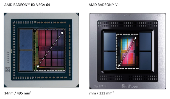
| Radeon VII |
Radeon 600 Mobile Series |
| Radeon RX Vega Series |
Radeon 500 Mobile Series |
| Radeon Pro Duo |
Radeon 400 Mobile Series |
| Radeon 600 Series |
Ryzen Mobile 2000 Series |
| Radeon RX 500 Series |
Ryzen Mobile 3000 Series |
| Radeon RX 400 Series |
Ryzen Mobile 4000 Series |
| Ryzen 5000G Series APUs |
Ryzen Mobile 5000 Series |
| Ryzen 4000G Series APUs |
Ryzen Mobile 7030U Series |
| Ryzen 3000G Series APUs |
|
| Ryzen 2000G Series APUs |
|
Meanwhile, things are a little more short-lived for the newer Vega GPU architecture (GCN 5). While AMD introduced the first discrete Vega GPUs and video cards in mid-2017 – and replaced the whole lot of them in mid-2019 – that GPU architecture remained in use in current-generation products for much longer as an integrated graphics solution. AMD’s current desktop APUs, the Ryzen 5000G series, integrate a Vega GPU. And the same silicon is still sold in the mobile space as the budget-minded Ryzen Mobile 7030 series. So although the Vega architecture is only a year younger than Polaris, it has stuck around for much longer overall.
Unfortunately, that does also mean that these Vega-based APUs are also getting something of the short end of the stick when it comes to driver support, receiving only a few years of mainstream driver support before being deprioritized. Though as these are also the weakest Vega GPUs, they’re admittedly also the least likely to be used with new games. More critical here will be how long AMD supplies security fixes for the Vega GPU architecture, especially since GPU drivers are popular targets for privilege escalation attacks.
In any case, while this isn’t a eulogy for the final members of the Graphics Core Next GPU architecture – at least, not quite yet – it’s clear that, 12 years later, GCN’s time is finally approaching its end.
Source: AnandTech – AMD Begins Polaris and Vega GPU Retirement Process, Reduces Ongoing Driver Support