Lenovo ThinkStation P360 Ultra Melds Desktop Alder Lake and NVIDIA Professional Graphics

Over the last decade or so, advancements in CPU and GPU architectures have combined extremely well with the relentless march of Moore’s Law on the silicon front. Together, these have resulted in hand-held devices that have more computing power than huge and power-hungry machines from the turn of the century. On the desktop front, small form-factor (SFF) machines are now becoming a viable option for demanding professional use-cases. CAD, modeling, and simulation capabilities that required big iron servers or massive tower workstations just a few years back are now capable of being served by compact systems.


Workstation notebooks integrating top-end mobile CPUs and professional graphics solutions from AMD (FirePro) or NVIDIA (Quadro Mobile / RTX Professional) have been around since the mid-2000s. The advent of UCFF and SFF PCs has slowly brought these notebook platforms to the desktop. Zotac was one of the early players in this market, and continues to introduce new products in the Zotac ZBOX Q Series. The company has two distinct lines – one with a notebook CPU and a professional mobile GPU (with a 2.65L volume), and another with a workstation CPU (Xeons up to 80W) and a professional mobile GPU (with a 5.85L volume).


Today, Lenovo is also entering the SFF workstation PC market with its ThinkStation P360 Ultra models. The company already has tiny workstations that do not include support for discrete GPUs, and that is fixed in the new Ultra systems. Featuring desktop Alder Lake with an Intel W680 chipset (allowing for ECC RAM option), these systems also optionally support discrete graphics cards – up to NVIDIA RTX A5000 Mobile. Four SODIMM slots allow for up to 128GB of ECC or non-ECC DDR5-4000 memory. Two PCIe Gen 4 x4 M.2 slots and a SATA III port behind a 2.5″ drive slot are also available, with RAID possibility for the M.2 SSDs. Depending on the choice of CPU and GPU, Lenovo plans to equip the system with one of three 89% efficiency external power adapters – 170W, 230W, or 300W.


The front panel has a USB 3.2 Gen 2 Type-A and two Thunderbolt 4 Type-C ports, as well as a combo audio jack. The vanilla iGPU version has four USB 3.2 Gen 2 Type-A ports, three DisplayPort 1.4 ports, and two RJ-45 LAN ports (1x 2.5 GbE, and 1x 1 GbE). On the WLAN front, the non-vPro option is the Wi-Fi 6 AX201, while the vPro one is the Wi-Fi 6E AX211. In addition to the PCIe 4.0 x16 expansion slot for the discrete GPU, the system also includes support for a PCIe 3.0 x4 card such as the Intel I350-T2 dual-port Gigabit Ethernet Adapter.


With dimensions of 87mm x 223mm x 202mm, the whole package comes in at 3.92L. In order to cram the functionality into such a chassis, Lenovo has employed a custom dual-sided motherboard with a unique cooling solution, as indicated in the teardown picture above. A blower fan is placed above the two M.2 slots to ensure that thte PCIe Gen 4 M.2 SSDs can operate without any thermal issues.


As is usual for Lenovo’s business / professional-oriented PCs, these systems are tested to military grade requirements and come with ISV certifications fro companies such as Autodesk, ANSYS, Dassault, PTC, Siemens, etc. Pricing starts at $1299 for the base model without a discrete GPU.


The ThinkStation P360 Ultra joins Lenovo’s already-announced P360 Tiny and the P360 Tower models. The P360 Tiny doesn’t support discrete GPUs, while the P360 Tower goes overboard with support for 3.5″ drives, and up to four PCIe expansion cards, along with a 750W PSU. Most workstation use-cases can get by without all those bells and whistles. Additional options for the end consumer are always welcome, and that is where the P360 Ultra comes into play.


Source: AnandTech – Lenovo ThinkStation P360 Ultra Melds Desktop Alder Lake and NVIDIA Professional Graphics

TSMC to Expand Capacity for Mature and Specialty Nodes by 50%

TSMC this afternoon has disclosed that it will expand its production capacity for mature and specialized nodes by about 50% by 2025. The plan includes building numerous new fabs in Taiwan, Japan, and China. The move will further intensify competition between TSMC and such contract makers of chips as GlobalFoundries, UMC, and SMIC.


When we talk about silicon lithography here at AnandTech, we mostly cover leading-edge nodes used produce advanced CPUs, GPUs, and mobile SoCs, as these are devices that drive progress forward. But there are hundreds of device types that are made on mature or specialized process technologies that are used alongside those sophisticated processors, or power emerging smart devices that have a significant impact on our daily lives and have gained importance in the recent years. The demand for various computing and smart devices in the recent years has exploded by so much that this has provoked a global chip supply crisis, which in turn has impacted automotive, consumer electronics, PC, and numerous adjacent industries.


Modern smartphones, smart home appliances, and PCs already use dozens of chips and sensors, and the number (and complexity) of these chips is only increasing. These parts use more advanced specialty nodes, which is one of the reason why companies like TSMC will have to expand their production capacities of otherwise “old” nodes to meet growing demand in the coming years.


But there is another market that is about to explode: smart cars. Cars already use hundreds of chips, and semiconductor content is growing for vehicles. There are estimates that several years down the road the number of chips per car will be about 1,500 units – and someone will have to make them. Which is why TSMC rivals GlobalFoundries and SMIC have been increasing investments in new capacities in the last couple of years.


TSMC, which has among the largest CapEx budgets in the semiconductor industries (which is challenged only by Samsung) has in recent years been relatively quiet about their mature and specialty node production plans. But at their 2022 TSMC Technology Symposium, the company outlined its plans formally.


The company is investing in four new facilities for mature and specialty nodes:


  • Fab 23 Phase 1 in Kumamoto, Japan. This semiconductor fabrication facility will make chips using TSMC’s N12, N16, N22, and N28 nodes and will have a production capacity of up to 45,000 300-mm wafer starts per month.
  • Fab 14 Phase 8 in Tainan, Taiwan.
  • Fab 22 Phase 2 in Kaohsiung, Taiwan.
  • Fab 16 Phase 1B in Nanjing, China. TSMC currently makes chips on its N28 in China, though the new phase was once rumored to be capable of making chips using more advanced nodes.


Increasing mature/specialized capacity by 50% over the next three years is a big shift for the company, and one that will improve TSMC’s competitive positions on the market. What is perhaps more important is that the company’s specialty nodes are largely based on its common nodes, which allows at least some companies to re-use IP they once developed for compute or RF for a new application. 


“[Our] specialty technology is quite unique as it is based on common technology platform  [logic technology platform], so our unique strategy is to allow our customer to share or reuse many of the [common] IP,” said Kevin Zhang, senior vice president of business development at TSMC. “For example, you have RF capability, you build that RF on a common logic platform, but later you find ‘hey someone need a so-called ULV feature to support an IoT product application.’ You want to build that on a common platform so you can allow different product lines to be able to share IP across the board, this is very important for our customers so we do want to provide a integrated platform to address the market needs of customer from product perspective.’ 


There are other advantages too. For example, TSMC’s N6RF allows chip designers to combine high-performance logic with RF, which enables them to build products such as modems and other, more unique solutions. Many companies are already familiar with TSMC’s N6 logic node, so now they have an opportunity to add RF connectivity to something that benefits from high performance. GlobalFoundries has a similar approach, but since the U.S.-based foundry does not have anything comparable to TSMC’s N6, TSMC has an indisputable advantage here.


With its common platform approach for mature nodes as well as specialized technologies, and 50% more capacity, TSMC will be able to offer the world more chips for smart and connected devices in the coming years. Furthermore, it will also benefit TSMC by significantly increasing the company’s revenues from mature and specialized nodes, as well as increasing pressure on their rivals.


Source: AnandTech – TSMC to Expand Capacity for Mature and Specialty Nodes by 50%

TSMC Unveils N2 Process Node: Nanosheet-based GAAFETs Bring Significant Benefits In 2025

At its 2022 Technology Symposium, TSMC formally unveiled its N2 (2 nm class) fabrication technology, which is slated to go into production some time in 2025 and will be TSMC’s first node to use gate-all-around field-effect transistors (GAAFETs). The new node will enable chip designers to significantly reduce the power consumption of their products, but the speed and transistor density improvements seem considerably less tangible.


TSMC’s N2 is a brand-new platform that extensively uses EUV lithography and introduces GAAFETs (which TSMC calls nanosheet transistors) as well as backside power delivery. The new gate-all-around transistor structure promises well-published advantages, such as greatly reduced leakage current (now that the gates are around all four sides of the channel) as well as ability to adjust channel width to increase performance or lower power consumption. As for the backside power rail, it is generally designed to enable better power delivery to transistors, offering a solution to the problem of increasing resistances in the back-end-of-line (BEOL). The new power delivery is slated to increase transistor performance and lower power consumption.


From feature set standpoint, TSMC’s N2 looks like a very promising technology. As for actual numbers, TSMC promises that N2 will allow chip designers to increase performance by 10% to 15% at the same power and transistor count, or reduce power consumption at the same frequency and complexity by 25% ~ 30%, all the while increasing chip density by over 1.1-fold when compared to N3E node.


Advertised PPA Improvements of New Process Technologies

Data announced during conference calls, events, press briefings and press releases
  TSMC
N5

vs

N7
N3

vs

N5
N3E

vs

N5
N2

vs

N3E
Power -30% -25-30% -34% -25-30%
Performance +15% +10-15% +18% +10-15%
Chip Density* ? ? ~1.3X >1.1X
Volume

Manufacturing
Q2 2022 H2 2022 Q2/Q3 2023 H2 2025


*Chip density published by TSMC reflects ‘mixed’ chip density consisting of 50% logic, 30% SRAM, and 20% analog. 


Versus N3E, the performance improvements and power reductions enabled by TSMC’s N2 node are in line with what the foundry’s new nodes typically bring in. But the so-called chip density improvements (which should reflect transistor density gains) are just a little over 10%, which is not particularly inspiring, especially considering that N3E already offers a slightly lower transistor density when compared to vanilla N3. Keeping in mind that SRAM and analog circuits barely scale these days, mediocre improvements in transistor density of actual chips should probably be expected these days. However, a chip density improvement of 10% in about three years is certainly not great news for GPUs and other chips that live or die based on rapidly increasing their transistor counts. 


Bearing in mind that by the time TSMC’s N2 enters production the company will also have the density-optimized N3S node, it would appear that the foundry will have two process technologies based on different types of transistors yet offering very similar transistor densities, something that has never happened before.


As usual, TSMC will offer their N2 node with various features and knobs to allow chip designers to optimize for things like mobile and high-performance computing designs (note that TSMC calls HPC everything that is not mobile, automotive or specialty. which includes everything from a low-power laptop CPU to a high-end compute GPU aimed at supercomputers). Also, platform offerings include something that TSMC calls ‘chiplet integration’, which probably means that TSMC enable its customers to easily integrate N2 chips into multi-chiplet packages made using various nodes. Since transistor density scaling is slowing down and new process technologies are getting more expensive to use, multi-chiplet packages are going to become more common in the coming years as developers will be using them to optimize their designs and costs.


TSMC expects to start risk production of chips using its N2 fabrication process sometimes in the second half of 2024, which means that the technology should be available for high volume manufacturing (HVM) of commercial products in the second half of 2025. But, considering the length of modern semiconductor production cycles, it’s likely more pragmatic to expect the first N2 chips to become available either very late in 2025 or 2026, if everything goes as planned.


Source: AnandTech – TSMC Unveils N2 Process Node: Nanosheet-based GAAFETs Bring Significant Benefits In 2025

TSMC Readies Five 3nm Process Technologies, Adds FinFlex For Design Flexibility

Taiwan Semiconductor Manufacturing Co. on Thursday kicked off its 2022 TSMC Technology Symposium, where the company traditionally shares it process technology roadmaps as well as its future expansion plans. One of the key things that TSMC is announcing today are its leading-edge nodes that belong to its N3 (3 nm class) and N2 (2nm class) families that will be used to make advanced CPUs, GPUs, and SoCs in the coming years.


N3: Five Nodes Over Next Three Years


As fabrication processes get more complex, their pathfinding, research, and development times get stretched out as well, so we no longer see a brand-new node emerging every two years from TSMC and other foundries. With N3, TSMC’s new node introduction cadence is going to expand to around 2.5 years, whereas with N2, it will stretch to around three years. 


This means that TSMC will need to offer enhanced versions of N3 in order to meet the needs of its customers who are still looking for a performance per watt improvement as well as transistor density bump every year or so. Another reason why TSMC and its customers need multiple versions of N3 is because the foundry’s N2 relies on all-new gate-all-around field-effect transistors (GAA FETs) implemented using nanosheets, which is expected to come with higher costs, new design methodologies, new IP, and many other changes. While developers of bleeding-edge chips will be quick to jump to N2, many of TSMC’s more rank & file customers will stick to various N3 technologies for years to come.


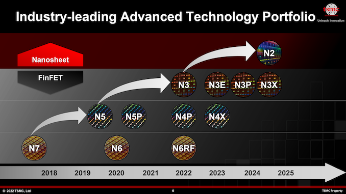
At its TSMC Technology Symposium 2022, the foundry talked about four N3-derived fabrication processes (for a total of five 3 nm-class nodes) — N3E, N3P, N3S, and N3X — set to be introduced over the coming years. These N3 variants are slated to deliver improved process windows, higher performance, increased transistor densities, and augmented voltages for ultra-high-performance applications. All these technologies will support FinFlex, a TSMC “secret sauce” feature that greatly enhances their design flexibility and allows chip designers to precisely optimize performance, power consumption, and costs. 


Advertised PPA Improvements of New Process Technologies

Data announced during conference calls, events, press briefings and press releases
  TSMC
N4

vs

N5
N4P

vs

N5
N4P

vs

N4
N4X

vs

N5
N4X

vs

N4P
N3

vs

N5
N3E

vs

N5
Power lower -22% ? ? -25-30% -34%
Performance higher +11% +6% +15%

or

more
+4%

or more
+10-15% +18%
Logic Area


Reduction* %


Logic Density*
0.94x


-6%


1.06x
0.94x


-6%


1.06x


?


?
0.58x


-42%


1.7x
0.625x


-37.5%


1.6x
Volume

Manufacturing
2022 2023 H2 2022 2023 2023 H2 2022 Q2/Q3 2023


*Note that TSMC only started to publish transistor density enhancements for analog, logic, and SRAM separately around 2020. Some of the numbers still reflect ‘mixed’ density consisting of 50% logic, 30% SRAM, and 20% analog. 


N3 and N3E: On Track for HVM


TSMC’s first 3 nm-class node is called N3 and this one is on track to start high volume manufacturing (HVM) in the second half of this year. Actual chips are set to be delivered to customers in early 2023.This technology is mostly aimed at early adopters (read: Apple and the like) who can invest in leading-edge designs and would benefit from the performance, power, area (PPA) advantages offered by leading-edge nodes. But as it’s tailored for particular types of applications, N3 has a relatively narrow process window (a range of parameters that produce a defined result), which may not be suitable for all applications in terms of yields.


This is when N3E comes into play. The new technology enhances performance, lowers power, and increases the process window, which results in higher yields. But the trade-off is that the node features a slightly reduced logic density. When compared to N5, N3E will offer a 34% reduction in power consumption (at the same speed and complexity) or an 18% performance improvement (at the same power and complexity), and will increase logic transistor density by 1.6x. 


It is noteworthy that, based on data from TSMC, N3E will offer higher clockspeeds than even N4X (due in 2023). However the latter will also support ultra-high drive currents and voltages of above 1.2V, at which point it will be able to offer unbeatable performance, but with very high power consumption. 


In general, N3E looks to be a more versatile node than N3, which is why it is not surprising that TSMC has more ‘3nm tape outs’ at this point than it had with its 5 nm-class node at a similar point of its development.


Risk production of chips using N3E is set to start in the coming weeks (i.e., in Q2 or Q3 2022) with HVM set for mid-2023 (again, TSMC does not disclose whether we are talking about Q2 or Q3). So expect commercial N3E chips to be available in late 2023 or early 2024.


N3P, N3S, and N3X: Performance, Density, Voltages


N3’s improvements do not stop with N3E. TSMC is set to bring out N3P, a performance-enhanced version of its fabrication process, as well as N3S, density-enhancing flavor of this node, some time around 2024. Unfortunately, TSMC is not currently disclosing what improvements these variants will offer compared to baseline N3. In fact, at this point TSMC does not even show N3S in all versions of its roadmap, so it is really not a good business to try guessing its characteristics.


Finally, for those customers who need ultra-high performance no matter power consumption and costs, TSMC will offer N3X, which is essentially an ideological successor of N4X. Again, TSMC is not revealing details about this node other than that it will support high drive currents and voltages. We might speculate that N4X could use backside power delivery, but since we are talking about a FinFET-based node and TSMC only going to implement backside power rail in GAAFET-based N2, we are not sure this is the case. Nonetheless, TSMC probably has a number of aces up its sleeve when it comes to voltage increases and performance enhancements.


FinFlex: N3’s Secret Sauce


Speaking of enhancements, we should definitely mention TSMC’s secret sauce for N3: FinFlex technology. In short, FinFlex allows chip designers to precisely tailor their building blocks for higher performance, higher density, and lower power.


When using a FinFET-based node, chip designers can choose between different libraries using different transistors. When developers need to minimize die size and save power at the cost of performance, they use double-gate single-fin (2-1) FinFETs (see the illustration). But when they need to maximize performance at the trade-off of die size and higher power, they use triple-gate dual-fin (3-2) transistors. When developers need a balance, they go with dual-gate dual-fin (2-2) FinFETs. 


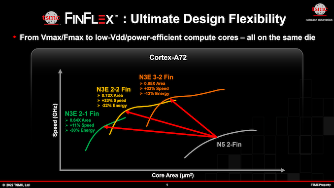
Currently, chip designers have to stick to one library/transistor type either for the whole chip or the whole block in a SoC design. For example, CPU cores can be implemented using 3-2 FinFETs to make them run faster, or 2-1 FinFETs to reduce their power consumption and footprint. This is a fair tradeoff, but it’s not ideal for all cases, especially when we are talking about 3 nm-class nodes that will be more expensive to use than existing technologies.


For N3, TSMC’s FinFlex technology will allow chip designers to mix and match different kinds of FinFETs within one block to precisely tailor performance, power consumption, and area. For complex structures like CPU cores, such optimizations give a lot of opportunities to increase core performance while still optimizing die sizes. So, we are eager to see how SoC designers will be able to take advantage of FinFlex in the looming N3 era.


FinFlex is not a substitute for node specialization (performance, density, voltages) as process technologies have greater differences than the ibraries or transistor structures within a single process technology, but FinFlex looks to be a good way to optimize performance, power, and costs for TSMC’s N3 node. Ultimately, this technology will bring the flexibility of FinFETs a little closer to that of GAAFETs, which are slated to offer adjustable channel widths to get higher performance or reduce power consumption.


Summary


Like TSMC’s N7 and N5, N3 will be another family of long-lasting nodes for the world’s largest contrast maker of semiconductors. Especially with the jump to GAAFETs coming up at 2nm for TSMC, the 3nm family will be the final family of “classic” leading-edge FinFET nodes from the firm, and one that a lot of customers will stick to for several years (or more). Which, in turn, is why TSMC is prepping multiple versions of N3 tailored for different applications – as well as FinFlex technology to give chip designers some additional flexibility with their designs.


The first N3 chips are set to enter production in the coming months and arrive to the market in early 2023. Meanwhile, TSMC will keep producing semiconductors using its N3 nodes long after it introduces its N2 process technology in 2025.


Source: AnandTech – TSMC Readies Five 3nm Process Technologies, Adds FinFlex For Design Flexibility

The ASUS ROG Maximus Z690 Hero Motherboard Review: A Solid Option For Alder Lake

Over the last six months since Intel launched its 12th Gen Core series of processors, we’ve looked at several Alder Lake desktop CPUs and seen how competitive they are from top to bottom – not just in performance but price too. To harness the power of Alder Lake, however, there are many options in terms of Z690 motherboards, and today we’re taking a look at one of ASUS’s more premium models, the ROG Maximus Z690 Hero.

They say hard times don’t create heroes, but ASUS has done for many years with good results. Equipped with plenty of top-tier features such as Thunderbolt 4, Intel’s Wi-Fi 6E CNVi, and support for up to DDR5-6400 memory, it has enough to make it a solid choice for gamers and enthusiasts. It’s time to see if the Z690 Hero option stacks up against the competition and if it can sparkle in a very competitive LGA1700 market.


Source: AnandTech – The ASUS ROG Maximus Z690 Hero Motherboard Review: A Solid Option For Alder Lake

Intel 4 Process Node In Detail: 2x Density Scaling, 20% Improved Performance

Taking place this week is the IEEE’s annual VLSI Symposium, one of the industry’s major events for disclosing and discussing new chip manufacturing techniques. One of the most anticipated presentations scheduled this year is from Intel, who is at the show to outline the physical and performance characteristics of their upcoming Intel 4 process, which will be used for products set to be released in 2023. The development of the Intel 4 process represents a critical milestone for Intel, as it’s the first Intel process to incorporate EUV, and it’s the first process to move past their troubled 10nm node – making it Intel’s first chance to get back on track to re-attaining fab supremacy.

Intel’s scheduled to deliver their Intel 4 presentation on Tuesday, in a talk/paper entitled “Intel 4 CMOS Technology Featuring Advanced FinFET Transistors optimized for High Density and High-Performance Computing”. But this morning, ahead of the show, they re publishing the paper and all of its relevant figures, giving us our first look at what kind of geometries Intel is attaining, as well as some more information about the materials being used.


Source: AnandTech – Intel 4 Process Node In Detail: 2x Density Scaling, 20% Improved Performance

AMD's Desktop CPU Roadmap: 2024 Brings Zen 5-based "Granite Ridge"

As part of AMD’s Financial Analyst Day 2022, it has provided us with a look at the company’s desktop client CPU roadmap as we advance towards 2024. As we already know, AMD’s latest 5 nm chips based on its Ryzen 7000 family are expected to launch in Fall 2022 (later this year), but the big news is that AMD has confirmed their Zen 5 architecture will be coming to client desktops sometime before the end of 2024 as AMD’s “Granite Ridge” chips.


At Computex 2022, during AMD’s Keynote presented by CEO Dr. Lisa Su, AMD unveiled its Zen 4 core architecture using TSMC’s 5 nm process node. Despite not announcing specific SKUs during this event, AMD did unveil some expected performance metrics that we could expect to see with the release of Ryzen 7000 for desktop. This includes 1 MB per core L2 cache, which is double the L2 cache per core with Zen 3, and up to a 15% performance uplight in single-threaded IPC performance. 


AMD 3D V-Cache Coming to Ryzen 7000 and Beyond


One key thing to note with AMD’s updated client CPU roadmap, it highlights some more on what to expect with its Zen 4 core, which is built on TSMC’s 5 nm node. AMD is expecting 8-10% IPC gains over Zen 3, on top of their previously announced clockspeed gains. As a result, the company is expecting single-threaded performance to improve by at least 15%, and by even more for multi-threaded workloads.


Meanwhile AMD’s 3D V-Cache packaging technology will also come to client desktop Zen 4. AMD is holding any further information close to their chest, but their current roadmap makes it clear that we should, at a minimum, expect a successor to the the Ryzen 7 5800X3D.


AMD Zen 5 For Client Desktop: Granite Ridge


The updated AMD client CPU roadmap until 2024 also gives us a time frame of when we can expect its next-generation Zen 5 cores. Built on what AMD is terming an “advanced node” (so either 4 nm or 3 nm), Zen 5 for client desktops will be Granite Ridge.


At two years out, AMD isn’t offering any further details than what they’ve said about the overall Zen 5 architecture thus far. So while we know that Zen 5 will involve a significant reworking of AMD’s CPU architecture with a focus on the front end and issue width, AMD isn’t sharing anything about the Granite Ridge family or related platform in particular. So sockets, chipsets, etc are all up in the air.


But for now, AMD’s full focus is on the Zen 4-based Ryzen 7000 family. Set to launch this fall, 2022 should end on a high note for the company.


Source: AnandTech – AMD’s Desktop CPU Roadmap: 2024 Brings Zen 5-based “Granite Ridge”

Updated AMD Notebook Roadmap: Zen 4 on 4nm in 2023, Zen 5 By End of 2024

As we’ve come to expect during AMD’s Financial Analyst Day (FAD), we usually get small announcements about big things coming in the future. This includes updated product roadmaps for different segments such as desktop, server, graphics, and mobile. In AMD’s latest notebook roadmap stretching out to 2024, AMD has unveiled that its mobile Zen 4 core (Pheonix Point) will be available sometime in 2023 and Zen 5 for mobile on an unspecified node which is expected to land sometime by the end of 2024.


The updated AMD Notebook roadmap through to 2024 highlights two already available mobile processors, the Zen 3-based Ryzen 5000 series with Vega integrated graphics and the latest Ryzen 6000 based on Zen 3+ and with the newest RDNA 2 mobile graphics capabilities. But there’s more that is due to be announced starting in 2023.


From The Rembrandt, Rises a Pheonix: Zen 4 Mobile AKA Pheonix Point


What’s new and upcoming on the updated AMD mobile roadmap is the successor to Rembrandt (Ryzen 6000), which AMD has codenamed Pheonix Point. AMD Phenoix Point will be based on AMD’s upcoming Zen 4 core architecture and will be built using TSMC’s 4 nm process node. According to the roadmap, AMD’s Zen 4 Pheonix Point mobile processors will use Artificial Intelligence Engine (AIE) and AMD’s upcoming and next-generation RDNA 3 integrated graphics. It’s unclear whether the platform will use DDR5 or DDR4 memory, but seeing as how Ryzen 7000 (Zen 4) uses the same core architecture and will be exclusive to DDR5 only that Pheonix Point will use DDR5 memory.


Also Announced: Zen 5 Mobile Codenamed Strix Point


Also on the AMD notebook roadmap is the announcement of its Zen 5-based platform on an unspecified manufacturing process, codenamed Strix Point. While details on Strix Point are minimal, AMD does state that Strix Point will use AMD’s unreleased RDNA 3+ graphics technology, which will likely be a refreshed and perhaps more performance per watt efficient RDNA 3 variation.


Also listed within the slide of the roadmap with Pheonix Point and Strix Point is an Artificial Intelligence Engine (AIE), which is more commonly found in mobile phones. The AI Engine or AIE will allow AMD to spec its products based on tiling with an adaptive interconnect. Still, it hasn’t unveiled much more about how it intends to incorporate AIE into its notebook portfolio. We know that it is part of AMD’s XDNA Adaptive Architecture IP, which comes from its acquisition of Xilinx.


We will likely learn more about AMD’s Pheonix Point based on Zen 4 in the coming future, as a release date sometime in 2023 is expected. As for Strix Point, which will be using its unannounced Zen 5 microarchitecture, we’re likely to hear more about this next year sometime.


Source: AnandTech – Updated AMD Notebook Roadmap: Zen 4 on 4nm in 2023, Zen 5 By End of 2024

AMD Announces Genoa-X: 4th Gen EPYC with Up to 96 Zen 4 Cores and 1GB L3 V-Cache

As AMD makes strides in snatching market share with its high-performance x86 processor designs in the server market, it has announced some of its upcoming 4th generations EPYC families expected sometime in 2023. Focusing on its technical computing and database-focused family codenamed Genoa-X, it is the direct successor to AMD’s Milan-X EPYC line-up which launches, later on, this year in Q4. 


Essentially the V-Cache enabled version of AMD’s Genoa EPYC CPUs, Genoa-X will include up to 96 Zen 4 cores and 1GB (or more) of L3 cache per socket. We know that Genoa-X will be using the latest SP5 socket (LGA6096), and will feature twelve memory channels, just like the regular Genoa platform which is set to debut in Q4 2022.


This means that the new SP5 platform will support Genoa, Genoa-X, Bergamo, and Siena, although it is unclear if users upgrading from Genoa to Genoa-X will need a new LGA6096 motherboard or if it will be enabled with a firmware update.


As the successor to Milan-X, Genoa-X is designed to slot into the same user segment, with AMD pitching it at customers who have workloads that uniquely benefit from oversized L3 caches – that is, workloads that can predominantly fit in those caches. That includes technical computing workloads (CAM, etc) as well as databases.


We expect to hear more about Genoa-X and any specific features it will bring to the 4th Gen EPYC platform in the future. AMD Genoa-X is scheduled to be released sometime in 2023.


Source: AnandTech – AMD Announces Genoa-X: 4th Gen EPYC with Up to 96 Zen 4 Cores and 1GB L3 V-Cache

AMD Unveils Siena, A Lower Cost EPYC Family With Up to 64 Zen 4 Cores

As part of AMD’s Financial Analyst Day 2022, AMD unveiled an updated server CPU roadmap up to and including 2024. Nestled within AMD’s latest server roadmap, it highlighted the Siena series, much like the Genoa (due Q4 2022), Bergamo (Due 1H 2023), and the Siena family from its 4th gen EPYC series are expected to land sometime in 2023. While roadmaps only give a glimpse of what is expected, they are used internally to plot and plan specific product groups and keep them on track for release.


The AMD Siena family of 4th generation EYPC processors are slightly different from Genoa and Genoa-X because Siena is primarily designed for the Edge and Telecommunication industries. Siena will feature up to 64 Zen 4 cores, and AMD states it will be a lower-cost platform in comparison to Genoa, Genoa-X, and Bergamo, all of which will be based on AMD’s Zen 4 core architecture and TSMC’s 5 nm and the even more highly optimized 4 nm process node.


AMD’s Siena family of EPYC 7004 products will likely be compatible with the SP5 platform that launches alongside Genoa in Q4 2022. SP5 features support twelve channels of DDR5 memory and PCIe 5.0 lanes, but it is unclear how AMD intends to package its Siena family in terms of die layout or whether it will feature a cut-down feature set to make it more affordable. 


We expect AMD to unveil more about Siena soon, and AMD states that Siena will be coming sometime in 2023.


Source: AnandTech – AMD Unveils Siena, A Lower Cost EPYC Family With Up to 64 Zen 4 Cores

AMD Updated EPYC Roadmap: 5th Gen EPYC "Turin" Announced, Coming by End of 2024

As part of AMD’s Financial Analysts Day 2022, AMD has provided updates to its Server CPU roadmap going into 2024. The biggest announcement is that AMD is already planning for the (next) next-gen core for its successful EPYC family, the 5th generation EPYC series, which has been assigned the codenamed Turin. Some key announcements include various segmentations of its expected EPYC 7004 portfolio, including Genoa, Bergamo, Genoa-X, and Siena.


From the launch of AMD’s EPYC 2nd generation products Codenamed Rome back in August 2019, the release of the updated EPYC 7003 processors, including both Milan and Milan-X, the next generation of EPYC 7004 codenamed Genoa is expected to launch in Q4 2022. Genoa will feature up to 96 Zen 4 cores based on TSMC’s 5 nm process node, with the new SP5 platform bringing support for 12-channel memory, PCIe 5.0, and support for memory expansion with Compute Express Link (CXL).


While Genoa will benefit from up to 96 Zen 4 cores and will be released towards the end of the year in Q4, AMD also announced Bergamo, which will be available in the first half of 2023, with Genoa-X and Siena also being available sometime in 2023. AMD’s Genoa-X will feature up to 96 Zen 4 cores based on TSMC’s 5 nm manufacturing node, with up to 1 GB of L3 cache per socket. AMD Siena will be predominantly targeted as a lower-cost platform and will feature up to 64 Zen 4 cores, with an optimized performance per watt, making it more affordable for the Edge and Telco markets.


AMD Unveils 5th Gen EPYC (Turin)


Perhaps the most significant announcement on AMD’s Server CPU Roadmap going into 2024 is the plan to bring its 5th generation of EPYC processors codenamed ‘Turin’ to market sometime before the end of 2024. As expected, AMD hasn’t shed many details on the Turin family of processors, but we expect it to be named the EPYC 7005 platform to follow its current EPYC name scheme.


We know that the Zen 5 cores will be based on a 4 nm mode (likely TSMC but not confirmed) and a 3 nm version, as highlighted in AMD’s CPU Core Roadmap through to 2024. AMD also states there will be three variants of the Zen 5 core in its CPU roadmap, including Zen 5, Zen 5 with 3D V-Cache, and Zen 5c.


From the latest roadmap highlighting AMD’s EPYC products, we know that AMD’s 5th generation of EPYC processors is expected to launch sometime before the end of 2024.


Source: AnandTech – AMD Updated EPYC Roadmap: 5th Gen EPYC “Turin” Announced, Coming by End of 2024

AMD: Combining CDNA 3 and Zen 4 for MI300 Data Center APU in 2023

Alongside their Zen CPU architecture and RDNA client GPU architecture updates, AMD this afternoon is also updating their roadmap for their CDNA server GPU architecture and related Instinct products. And while CPUs and client GPUs are arguably on a rather straightforward path for the next two years, AMD intends to shake up its server GPU offerings in a big way.

Let’s start first with AMD’s server GPU architectural roadmap. Following AMD’s current CDNA 2 architecture, which is being used in the MI200 series Instinct Accelerators, will be CDNA 3. And unlike AMD’s other roadmaps, the company isn’t offering a two-year view here. Instead, the server GPU roadmap only goes out one year – to 2023 – with AMD’s next server GPU architecture set to launch next year.

Our first look at CDNA 3 comes with quite a bit of detail. With a 2023 launch AMD isn’t holding back on information quite as much as they do elsewhere. As a result, they’re divulging information on everything from the architecture to some basic information about one of the products CDNA 3 will go in to – a data center APU made of CPU and GPU chiplets.


Source: AnandTech – AMD: Combining CDNA 3 and Zen 4 for MI300 Data Center APU in 2023

AMD’s 2022-2024 Client GPU Roadmap: RDNA 3 This Year, RDNA 4 Lands in 2024

Among the slew of announcements from AMD today around their 2022 Financial Analyst Day, the company offering an update to their client GPU (RDNA) roadmap. Like the company’s Zen CPU architecture roadmap, AMD has been keeping a 2 year horizon here, essentially showing what’s out, what’s about to come out, and what’s going to be coming out in a year or two. Meaning that today’s update gives us our first glace at what will follow RDNA 3, which itself was announced back in 2020.

With AMD riding a wave of success with their current RDNA 2 architecture products (the Radeon RX 6000 family), the company is looking to keep up that momentum as they shift towards the launch of products based on their forthcoming RDNA 3 architecture.  And while today’s roadmap update from AMD is a high-level one, it none the less offers us the most detailed look yet into what AMD has in store for their Radeon products later this year.


Source: AnandTech – AMD’s 2022-2024 Client GPU Roadmap: RDNA 3 This Year, RDNA 4 Lands in 2024

AMD RDNA 3/Navi 3X GPU Update: 50% Better Perf-Per-Watt, Using Chiplets For First Time

Continuing our coverage of AMD’s 2022 Financial Analyst day, we have the matter of AMD’s forthcoming RDNA 3 GPU architecture and the Navi 3X GPUs that will be built upon it. Up until now, AMD has been fairly quiet about what to expect with RDNA 3, but as RDNA 2 approaches its second birthday and the first RDNA 3 products are slated to launch this year, AMD is offering some of the first significant details on the GPU architecture.


First and foremost, let’s talk about performance. The Navi 3X family, to be built on a 5nm process (TSMC’s, no doubt) is targeting a greater-than 50% performance-per-watt uplift versus RDNA 2. This is a significant and similar uplift as to AMD saw moving from RDNA (1) to RDNA 2. And while such a claim from AMD would have seemed ostentatious two years ago, RDNA 2 has given AMD’s GPU teams a significant amount of renewed credibility.


Thankfully for AMD, unlike the 1-to-2 transition, they don’t have to find a way to come up with a 50% uplift based on architecture and DVFS optimizations alone. The 5nm process means that Navi 3X is getting a full node’s improvement from the TSMC N7/N6 based Navi 2X GPU family. As a result, AMD will see a significant efficiency improvement from that alone.


But with that said, these days a single node jump on its own can’t deliver a 50% perf-per-watt improvement (RIP Dennard scaling). So there are several architecture improvements planned for RDNA 3. This includes the next generation of AMD’s on-die Infinity Cache, and what AMD is terming an optimized graphics pipeline. According to the company, the GPU compute unit (CU) is also being rearchitected, though to what degree remains to be seen.


But the biggest news of all on this front is that, confirming a year’s worth of rumors and several patent applications, AMD will be using chiplets with RDNA 3. To what degree, AMD isn’t saying, but the implication is that at least one GPU tier (as we know it) is moving from a monolithic GPU to a chiplet-style design, using multiple smaller chips.


Chiplets are in some respects the holy grail of GPU construction, because they give GPU designers options for scaling up GPUs past today’s die size (reticle) and yield limits. That said, it’s also a holy grail because the immense amount of data that must be passed between different parts of a GPU (on the order of terabytes per second) is very hard to do – and very necessary to do if you want a multi-chip GPU to be able to present itself as a single device. We’ve seen Apple tackle the task by essentially bridging two M1 SoCs together, but it’s never been done with a high-performance GPU before.


Notably, AMD calls this an “advanced” chiplet design. That moniker tends to get thrown around when a chip is being packaged using some kind of advanced, high-density interconnect such as EMIB, which differentiates it from simpler designs such as Zen 2/3 chiplets, which merely route their signals through the organic packaging without any enhanced technologies. So while we’re eagerly awaiting further details of what AMD is doing here, it wouldn’t at all be surprising to find out that AMD is using a form of Local Si Interconnect (LSI) technology (such as the Elevated Fanout Bridge used for the MI200 family of accelerators) to directly and closely bridge two RNDA 3 chiplets.


At this point, AMD isn’t going into any more details on the architecture or Navi 3X GPUs. Today is a teaser and roadmap update for the analyst market, not an announcement of what we can only assume will be the Radeon RX 7000 family of video cards. None the less, with the first RDNA 3 products slated to launch later this year, a more formal announcement cannot be too far away. So we’re looking forward to hearing more about what stands to be a major shake-up in the nature of GPU design and fabrication.


Source: AnandTech – AMD RDNA 3/Navi 3X GPU Update: 50% Better Perf-Per-Watt, Using Chiplets For First Time

AMD Zen Architecture Roadmap: Zen 5 in 2024 With All-New Microarchitecture

Today is AMD’s Financial Analyst Day, the company’s semi-annual, analyst-focused gathering. While the primary purpose of the event is for AMD to reach out to investors, analysts, and others to demonstrate the performance of the company and why they should continue to invest in the company, FAD has also become AMD’s de-facto product roadmap event. After all, how can you wisely invest in AMD if you don’t know what’s coming next?


As a result, the half-day series of presentations is full of small nuggets of information about products and plans across the company. Everything here is high-level – don’t expect AMD to hand out the Zen 4 transistor floorplan – but it’s easily our best look at AMD’s product plans for the next couple of years.


Kicking off FAD 2022 with what’s always AMD’s most interesting update is the Zen architecture roadmap. The cornerstone of AMD’s recovery and resurgence into a competitive and capable player in the x86 processor space, the Zen architecture is the basis of everything from AMD’s smallest embedded CPUs to their largest enterprise chips. So what’s coming down the pipe over the next couple of years is a very big deal for AMD, and the industry as a whole.


Source: AnandTech – AMD Zen Architecture Roadmap: Zen 5 in 2024 With All-New Microarchitecture

AMD Zen 4 Update: 8% to 10% IPC Uplift, 25% More Perf-Per-Watt, V-Cache Chips Coming

As part of today’s AMD’s 2022 Financial Analyst Day, the company is offering a short, high-level update on their forthcoming Zen 4 CPU architecture. This information is being divulged as part of the company’s larger Zen architecture roadmap, which today is being extended to announce Zen 5 for 2024.


The biggest news here is that AMD is, for the first time, disclosing their IPC expectations for the new architecture. Addressing some post-Computex questions around IPC expectations, AMD is revealing that they expect Zen 4 to offer an 8-10% IPC uplift over Zen 3. The initial Computex announcement and demo seemed to imply that most of AMD’s performance gains were from clockspeed improvements, so AMD is working to respond to that without showing too much of their hand months out from the product launches.


This makes up a good chunk of AMD’s overall >15% expected improvement in single-threaded performance, which was previously disclosed at Computex and essentially remains unchanged. That said, AMD is strongly emphasizing the “greater than” aspect of that performance estimate. At this point AMD can’t get overly specific since they haven’t locked down final clockspeeds, but as we’ve seen with their Computex demos, peak clockspeeds of 5.5GHz (or more) are currently on the table for Zen 4.


AMD is also talking a bit more about power and efficiency expectations today. At this point, AMD is projecting a >25% increase in performance-per-watt with Zen 4 over Zen 3 (based on desktop 16C chips running CineBench). Meanwhile the overall performance improvement stands at >35%, no doubt taking advantage of both the greater performance of the architecture per-thread, and AMD’s previously disclosed higher TDPs (which are especially handy for uncorking more performance in MT workloads). And yes, these are terrible graphs.


Finally, AMD is confirming that there will be V-Cache equipped Zen 4 SKUs within their processor lineup. No specific SKUs are being announced today, but AMD is reiterating that V-Cache was not just a one-off experiment for the company, and that they will be employing the die stacked L3 cache on some Zen 4 chips as well.


Source: AnandTech – AMD Zen 4 Update: 8% to 10% IPC Uplift, 25% More Perf-Per-Watt, V-Cache Chips Coming

Supermicro SYS-E100-12T-H Review: Fanless Tiger Lake for Embedded Applications

Compact passively-cooled systems find application in a wide variety of market segments including industrial automation, IoT gateways, digital signage, etc. These are meant to be deployed for 24×7 operation in challenging environmental conditions. Supermicro has a number of systems targeting this market under the Embedded/IoT category. Their SuperServer E100 product line makes use of motherboards in the 3.5″ SBC form-factor. In particular, the E100-12T lineup makes use of embedded Tiger Lake-U SoCs to create powerful, yet compact and fanless systems. Today’s review takes a look at the top-end of this line – the SYS-E100-12T-H based on the Intel Core i7-1185GRE embedded processor.


Source: AnandTech – Supermicro SYS-E100-12T-H Review: Fanless Tiger Lake for Embedded Applications

Apple Announces M2 SoC: Apple Silicon for Macs Updated For 2022

Though primarily a software-focused event, Apple’s WWDC keynotes are often stage for an interesting hardware announcement or two as well, and this year Apple did not disappoint. At the company’s biggest Mac-related keynote of the year, Apple unveiled the M2, their second-generation Apple Silicon SoC for the Mac (and iPad) platform. Touting modest performance gains over the original M1 SoC of around 18% for multithreaded CPU workloads and 35% in peak GPU workloads, the M2 is Apple’s first chance to iterate on their Mac SoC to incorporate updated technologies, as well as to refresh their lower-tier laptops in the face of recent updates from their competitors.

With the king of the M1 SoCs, M1 Ultra, not even 3 months behind them, Apple hasn’t wasted any time in preparing their second generation of Apple Silicon SoCs. To that end, the company has prepared what is the first (and undoubtedly not the last) of a new family of SoCs with the Apple Silicon M2. Designed to replace the M1 within Apple’s product lineup, the M2 SoC is being initially rolled out in refreshes of the 13-inch MacBook Pro, as well as the MacBook Air – which is getting a pretty hefty redesign of its own in the process.

The launch of the M2 also gives us our first real glimpse into how Apple is going to handle updates within the Apple Silicon ecosystem. With the iPhone family, Apple has kept to a yearly cadence for A-series SoC updates; conversely, the traditional PC ecosystem is on something closer to a 2-year cadence as of late. M2 seems to split this down the middle, coming about a year and a half after the M1 – though in terms of architecture it looks closer to a yearly A-series SoC update.


Source: AnandTech – Apple Announces M2 SoC: Apple Silicon for Macs Updated For 2022

The Apple WWDC 2022 Keynote Live Blog (Starts at 10am PT/17:00 UTC)

As we round the corner after Computex and transition into June, it’s time once more for Apple’s annual World Wide Developers Conference. As always, Apple kicks off WWDC with their big keynote event, which though aimed first and foremost at developers, is also used as a venue to announce new products and ecosystem strategies. The keynote starts at 10am Pacific (17:00 UTC) today, and AnandTech will be offering live blog coverage of Apple’s event.


With WWDC going virtual once again this year, we’re expecting another rapid-fire, two-hour run through of Apple’s ecosystem. WWDC keynotes have historically covered everything from macOS and iOS to individual Apple applications and more. On the hardware side of matters, in previous years we’ve seen things like the official announcement of Apple’s shift from x86 to Apple Silicon; and while 2021 was light on hardware, one never quite knows what Apple has in store. Apple has yet to launch an Arm-based Mac Pro, so there’s still some big surprises left in their bag, and of course there’s always the chance of the periodic product refresh.


So join us at 10am Pacific to see just what Apple is working on for this year and beyond.


Source: AnandTech – The Apple WWDC 2022 Keynote Live Blog (Starts at 10am PT/17:00 UTC)

Destination 30 TB: HDD Vendors Plan Different Routes Hit Storage Milestone in 2023

In the recent months all three hard drive manufacturers — Seagate, Toshiba, and Western Digital — and some of their partners have outlined plans to ship 30TB HDDs already in 2023 ~ 2024 timeframe. Apparently, all of these companies plan to use different technologies to get to this milestone.


Demand for high capacity nearline hard drives has been increasing for years and is not going to stop, as more data is generated each and every day. But nearline HDD users not only want their drives in large quantities, but they want a rapid increase in capacity as well, in a bid to keep the number of drives (and therefore the number of servers and power consumption of datacenters) in check. But capacity increases have been slowing down in the recent years, mainly because of slow roll out of energy-assisted magnetic recording (EAMR) technologies. 


Source: AnandTech – Destination 30 TB: HDD Vendors Plan Different Routes Hit Storage Milestone in 2023