AMD Quietly Introduces Ryzen 3 5100 Quad-Core Processor For AM4

Further to AMD’s latest Micro Center exclusive processor, the Ryzen 5 5600X3D with 3D V-Cache, AMD has seemingly introduced a budget-focused quad-core processor based on their Zen 3 architecture. Officially confirmed via GIGABYTE’s CPU support pages for their AM4 motherboards, an unannounced Zen 3 CPU is listed in the way of the Ryzen 3 5100 processor.


Despite offering a wide variety of their latest Ryzen 7000 chips based on the Zen 5 architecture, AMD looks to be making good on their promise of still supporting their AM4 platform as we advance, but how many more chips are still to come remains to be seen. Despite its growing age, the AM4 platform still offers exceptional value for money, primarily through their X3D chips with additional 3D packaged V-Cache.


Despite AMD offering no official clarification on the launch of the Ryzen 3 5100, GIGABYTE is listing this processor through its official CPU support lists on their AM4 motherboards, which confirms this chip exists. When a processor makes it onto a CPU support list, this means that the processors in question, such as the Ryzen 7 5700 and Ryzen 3 5100, have been tested on the relevant platform and motherboard to confirm compatibility, as well as operating at the intended specifications by the processor manufacturer; in this case, AMD.


GIGABYTE also lists the Ryzen 7 5700, which appears to be a ‘new’ SKU, at least because it has been unobtainable through retail channels. This isn’t the case, as AMD confirmed that the Ryzen 7 5700, based on the same Cezanne Core typically found on AMD’s Ryzen 5000 chips bearing the G nomenclature, has been available through OEM partners. One example is a variant of CyberPower’s Gamer Master desktop system, which has the Ryzen 7 5700 and an NVIDIA GeForce RTX 3060 graphics card. 


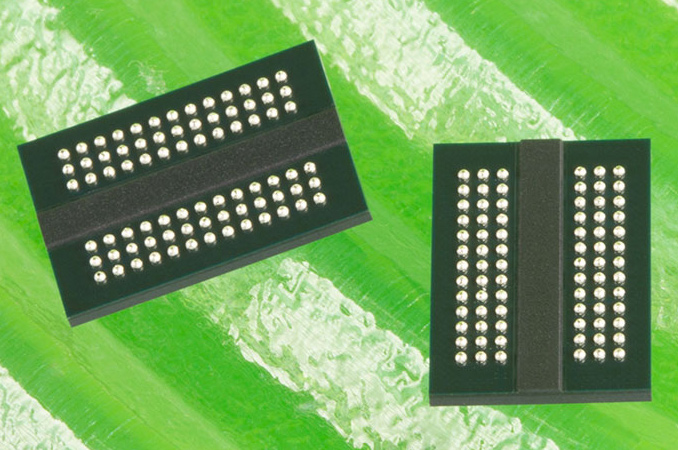
Touching more on the Cezanne core, the G nomenclature denotes that the chip has integrated graphics. These were part of AMD’s APU line-up, which included solid entry-level integrated graphics alongside the current generation cores taken from the regular desktop series. Although the typical Vermeer cores were the mainstay of the Zen 3 desktop processors, it’s possible that AMD recycled some of its APUs for the Ryzen 7 5700 and Ryzen 3 5100, which is one reason they might have the Cezanne cores but without the integrated graphics.


AMD Ryzen 5000 Series Processors for Desktop

(Zen 3) As of 07/11/23
AnandTech Core/

Thread
Base

Freq
1T

Freq
L3

Cache
Core uArch iGPU TDP Price

(Amazon)
Ryzen 9 5950X 16 32 3400 4900 64 MB Vermeer 105 W $440
Ryzen 9 5900X 12 24 3700 4800 64 MB Vermeer 105 W $275
Ryzen 9 5900 12 24 3000 4700 64 MB Vermeer 65 W OEM
 
Ryzen 7 5800X3D 8 16 3400 4500 96 MB Vermeer 105 W $278
Ryzen 7 5800X 8 16 3800 4700 32 MB Vermeer 105 W $236
Ryzen 7 5800 8 16 3400 4600 32 MB Vermeer 65 W OEM
 
Ryzen 7 5700X 8 16 3400 4600 32 MB Vermeer 65 W $174
Ryzen 7 5700G 8 16 3800 4600 16 MB Cezanne 8CU, 2000 MHz 65 W $178
Ryzen 7 5700 8 16 3700 4600 16 MB Cezanne 65 W OEM
 
Ryzen 5 5600X3D 6 12 3300 4400 96 MB Vermeer 105 W $230*
Ryzen 5 5600X 6 12 3700 4600 32 MB Vermeer 65 W $134
Ryzen 5 5600 6 12 3500 4400 32 MB Vermeer 65 W OEM
Ryzen 5 5600G 6 12 3900 4400 16 MB Cezanne 7CU, 1900 MHz 65 W $129
 
Ryzen 3 5300G 4 8 4000 4200 8 MB Cezanne 6CU, 1700 MHz 65 W
Ryzen 3 5100 4 8 3800 4200 8 MB Cezanne 65 W ?


*AMD Ryzen 5 5600X3D is a Micro Center Exclusive processor.


The AMD Ryzen 3 5100 is an entry-level quad-core (4C/8T) offering, which is also based on AMD’s APU-focused Cezanne microarchitecture. Outside of the Ryzen 5000G series of chips, the Ryzen 3 5100 is also the only quad-core variant for desktops from the 5000 series that doesn’t feature integrated graphics. The Ryzen 3 5100 comes with a modest 8 MB of L3 cache, a base frequency of 3.8 GHz. a boost frequency of up to 4.2 GHz, support for DDR4-3200 memory, and a 65 W TDP.


Despite the Ryzen 7 5700 not being available in retail channels, the Ryzen 7 5700 (8C/16T) is only available through OEM channels, and Ryzen 3 5100 (4C/8T) looks to bolster the already extensive selection of chips compatible with AMD’s AM4 platform. It is worth noting that these chips have been supported on GIGABYTE’s B550 Gaming X motherboard since BIOS revision F14, which is a more recent update as GIGABYTE’s AM4 platform is currently sitting on the F16c firmware at the time of writing.


Touching on availability, the Ryzen 3 5100 was meant to be part of a selection of chips due to launch last year around the same time as the Ryzen 7 5800X3D did in April 2022. Alas, that did not happen as expected, and we did reach out to AMD, who confirmed the Ryzen 7 5700 has been available in OEM channels since last year. The Ryzen 3 5100 could be OEM only, but there are no examples of this chip in any OEM partner systems (not that we can find), and AMD remains tight-lipped on its existence or availability.


Source: AnandTech – AMD Quietly Introduces Ryzen 3 5100 Quad-Core Processor For AM4

Intel Set to Exit NUC PC Business – Pushes Partners to Develop More SFF PCs

Intel has disclosed today that it will halt further development of its small form factor Next Unit of Compute (NUC) PCs. The tech giant expects its partners to take over and keep serving markets served by its NUC systems as it focuses on much more profitable chips businesses. 


“We have decided to stop direct investment in the Next Unit of Compute (NUC) Business and pivot our strategy to enable our ecosystem partners to continue NUC innovation and growth,” a statement by Intel reads. “This decision will not impact the remainder of Intel’s Client Computing Group (CCG) or Network and Edge Computing (NEX) businesses. Furthermore, we are working with our partners and customers to ensure a smooth transition and fulfillment of all our current commitments – including ongoing support for NUC products currently in market.”


Intel entered PC business with its ultra-compact NUC desktops in 2013, around the time it exited motherboards market. Initially, the company only targeted SOHO market with its NUC barebones and PCs, but eventually it greatly expanded its NUC range with systems aimed at corporate users that need things like remote management and appropriate support, and even gaming machines. 


Intel’s NUC systems have garnered considerable popularity over the years, going toe-to-toe with similar offerings from established PC brands. While small form factor existed before the NUC (and will exist after), Intel’s efforts to invigorate the space with its NUC designs were by and large successful, and a lot of the public experimentation we’ve seen done in the space over the last several years has come from Intel.


Nevertheless, maintaining a wide variety of desktops and laptop platforms has been somewhat taxing (if not distracting) for Intel, whose primary focus lies in the semiconductor industry, rather than finished devices.


While Intel isn’t citing any specific reasons in their decision to wrap up development of new NUC PCs, given the contracting PC market and the intense rivalry therein, we wouldn’t be surprised if Intel was being rocked by the same market forces that have been putting a squeeze on other PC OEMs. Intel has already reduced its focus on NUCs in the recent years, never offering Performance versions of its 12th and 13th Generation NUCs – and we cannot say that that those machines were missed by the audience. Meanwhile, Intel’s enthusiast-grade Extreme NUCs have evolved to be more like fully-fledged desktops rather than compact systems, getting farther and farther away from the NUC’s tiny roots. And while the add-in card form-factor used by the NUC Extreme lineup has always looked promising, it is unclear whether they have even been a success for Intel.


Ultimately, as Intel has continued to shed and shutter non-core businesses, it is not entirely unexpected that Intel is axing its NUC program. In its place, the company is urging its OEM/ODM partners – whose bread and butter is designing and selling complete systems – to continue producing and innovating on compact machines for the small office/home office market, business clientele, and gamers. This leaves Intel free to refocus on the highly lucrative chip manufacturing business, as CEO Pat Gelsinger has made a priority over the past couple of years.


Intel’s NUC will not be the first business divested by Intel in the recent years. To focus on development on leading-edge CPUs, GPUs, and other lucrative products, Intel left the NAND memory and SSD businesses, axed Optane SSDs, ceased development of notebook models, and even sold its prebuilt server business to MiTAC.


Source: AnandTech – Intel Set to Exit NUC PC Business – Pushes Partners to Develop More SFF PCs

El Capitan's Little Brother Tuolumne Can Conquer Most Top 10 Supercomputers

Lawrence Livermore National Laboratory (LLNL) started to install its El Capitan supercomputer that promises to achieve computational performance of over 2 FP64 ExaFLOPS for classified national security research. Parallel to this, the LLNL also plans to introduce a less potent but still extremely fast supercomputer named Tuolumne. This companion model will be dedicated to unclassified research and will offer 10% to 15% of El Capitan’s computational prowess, which is still enough to beat most of the systems in the current Top500 supercomputer list.


While LLNL’s El Capitan will not be the first exascale system and will not even be the first to break 2 FP64 ExaFLOPS performance record, it is still a very special system as it will be the first exascale supercomputer to use AMD’s Instinct MI300A accelerated processing units comprising of Zen 4 x86 cores and CDNA 3-based compute GPUs. When El Capitan goes online, it will substantially outpace Frontier, the world’s fastest PC, which is rated for an Rpeak performance of 1.679 FP64 ExaFLOPS.


Tuolumne is expected to use similar architecture to El Capitan, so it will also use Instinct MI300A APU. Even with just a tenth of El Capitan’s performance, Tuolumne will join the upper echelons of the global supercomputers list, capable of delivering 200 PetaFLOPS. This potential performance could place it among the Top 10 supercomputers listed in the current Top 500 list. Still, if it manages to deliver 15% of El Capitan’s performance, it could rival Leonardo, a supercomputer powered by Intel Xeon Platinum 8358 and Nvidia A100 with an Rpeak performance of 304.47 PetaFLOPS, which is currently ranked as the fourth fastest supercomputer.


We are planning to get an unclassified system that will be called Tuolumne,” said Bronis R. de Supinski in an interview with ExaScaleProject.org. De Supinski is the chief technology officer for Livermore Computing at LLNL. “It will be roughly between 10% to 15% the size of El Capitan.


Supercomputers with classified status, like the existing Sierra and the planned El Capitan at LLNL, primarily serve national security needs. According to Bronis R. de Supinski, El Capitan will be mainly used for the stockpile stewardship program, ensuring the reliability of nuclear weapons without resorting to real testing. Conversely, unclassified supercomputers, like the upcoming Tuolumne, serve diverse computational requirements spanning various scientific fields, from research and engineering simulations to data analysis and weather prediction.


Tuolumne will be contributing more to the wider range of scientific areas,” de Supinski added. “There’s a lot of materials modeling. We have typically had a wide range of molecular dynamics. Some QCD get run on the system, seismic modeling. What will probably happen is that you know, those sorts of applications, climate, and that sort of thing will run on Tuolumne. And if there is a particular case to be made, we can occasionally provide for briefer runs on the big system.


Source: ExaScaleProject.org


Source: AnandTech – El Capitan’s Little Brother Tuolumne Can Conquer Most Top 10 Supercomputers

Adata Reveals Its First PCIe Gen5 SSD: Legend 970

Adata has introduced its first PCIe 5.0 SSD, the Legend 970. A Phison E26-based design, the Legend 970 pairs Phison’s high-end controller with a sophisticated active cooling system that promises predictable performance even under high loads. The Legend 970 SSD is aimed at high-performance desktops that can take advantage of fast storage devices.


Adata’s Legend 970 drives come in 1 TB and 2 TB capacities and are rated for an up to 10,000 MB/s sequential read/write speed as well as a 1.4 million random read/write IOPS, performance levels in line with those of many current-generation enterprise-grade SSDs. The drives fully support all modern SSD technologies that one comes to expect from a contemporary drive, including SLC cache, Low Density Parity Check Code (LDPC) error correction, and AES 256-bit high-level encryption.


Like other PCIe Gen 5 SSDs available now, the Legend 970 product uses Phison’s PS5026-E26 controller. As for memory, the drives use Micron’s 232-layer TLC NAND with a 1600 MT/s interface.


One of the key selling points of Adata’s Legend 970 is its cooling system, which although a bit on the bulky side of matters, is designed to be robust enough to keep the drive from thermal throttling even under high, sustained loads. Though at 80.6×24.2×17.9mm in size, the resulting SSD is decided a desktop part – and even then the drive will need a fair bit of clearance to fit.


Adata’s iniital Legend 970 SSD will eventually be joined by at least one other PCIe 5.0 SSD as well. The company’s XPG division is working on their NeonStorm SSD, which uses a self-contained liquid cooling system, and is rated for read speeds of up to 14GB/second (thanks to TLC NAND with a 2400 MT/s interface).


Adata’s Legend 970 drives will come with a five-year global warranty. The company hasn’t published any pricing information, though we’d expect the drives to be more or less in line with other first-generation PCIe Gen5 SSDs.


Source: AnandTech – Adata Reveals Its First PCIe Gen5 SSD: Legend 970

El Capitan Installation Begins: First APU-based Exascale System Shaping Up For 2024

Lawrence Livermore National Laboratory had received the first components of its upcoming El Capitan supercomputer and begun to install them, the laboratory announced on Wednesday. The system is set to come online in mid-2024 and is expected to deliver performance of over 2 ExaFLOPS.


LLML’s El Capitan is based on Cray’s Shasta supercomputer architecture and will be built by HPE, just like two other exascale systems in the U.S., Frontier and Aurora. Unlike the first two exascale machines, which use a traditional discrete CPU plus discrete GPU configuration, the El Capitan supercomputer will be the first one based on AMD server-grade APUs that integrate both processor types in to a single, highly connected package.


AMD’s Instinct MI300A APU incorporates both CPU and GPU chiplets, offering 24 general-purpose Zen 4 cores, compute GPUs powered by the CDNA 3 architecture, and 128 GB of unified on-package HBM3 memory. AMD has been internally evaluating its Instinct MI300A APU for months, and it appears that AMD and HPE are now ready to start installing the first pieces of hardware that make up El Capitan.


According to pictures released by the Lawrence Livermore National Laboratory, its engineers have already put a substantial number of servers into racks. Though LLNL’s announcement leaves it unclear whether these are “completed” servers with production-quality silicon, or pre-production servers that will be filled out with production silicon at a later date. Notably, parts of Aurora were initially assembled with pre-production CPUs, which were only swapped out for Xeon CPU Max chips over the past couple of months. Given the amount of validation work required to stand-up a world-class supercomputer, AMD and HPE may be employing a similar strategy here.


“We have begun receiving & installing components for El Capitan, first #exascale #supercomputer,” a Tweet by LLNL reads. “While we are still a ways from deploying it for national security purposes in 2024, it is exciting to see years of work becoming reality.”


When it comes online in 2024, LLNL is expecting El Capitan to be the fastest supercomputer in the world. Though with its full specifications still being held back, it’s not clear how much faster it is on paper compared to the 2 EFLOPS Aurora – let alone real-world performance. Part of the design goal of AMD’s MI300A APU is to exploit additional performance efficiency gains that come from placing CPU and GPU blocks so close together, so it will be interesting to see what the software development teams programming for El Capitan can achieve, especially as they get their software further optimized.


LLNL’s El Capitan is expected to cost $600 million. The system will be used nuclear weapons simulations and will be crucial for the U.S. national security. It replaces Sierra, a supercomputer based on IBM Power 9 and NVIDIA Volta accelerators, and promises to offer performance that is 16 times higher.


Source: AnandTech – El Capitan Installation Begins: First APU-based Exascale System Shaping Up For 2024

ASRock Goes Low-Profile with New Arc A380 Graphics Card

As Intel’s slate of video card board partners has expanded over the last year, so has the variety in the ecosystem, as the newly minted partners set out to design their own unique products around Intel’s fledgling GPU family. This, thankfully, is starting to include some underserved markets such as low profile vide cards, which have been left behind in the focus on bigger-and-better video cards. Which brings us to ASRock’s latest Arc A380 graphics card, a new low-profile A380 design that brings Intel’s entry-level discrete GPU to smaller systems.


As far as specifications are concerned, ASRock’s Arc A380 Low Profile 6GB (A380 LP 6G) is a typical Arc A380 product that carries Intel’s ACM-G11 GPU (1024 stream processors, 2.0 GHz) coupled with 6GB of GDDR6 memory attached via a 96-bit interface. Remarkably, the card maintains a TDP below 75W, which eliminates the need for an extra power connector. This makes it a potential upgrade for small form factor machines and older PCs that do not have a spare PCIe power connector.


It should be noted, however, that while the A380 LP 6G is a low-profile card, it is still a relatively powerful card, necessitating a dual-slot cooler. So while the card should work with the majority of compact PCs, it may still be a bit too big for the smallest of systems.


The low-profile design of the ASRock Arc A380 graphics card suggests that it is not necessarily targeting even entry-level gaming machines. Instead, it appears to be a reasonable choice for minimalist office PCs and home theater PCs (HTPCs). Speaking of office PCs, ASRock’s Arc A380 Low Profile 6GB graphics card only has two display outputs: one DisplayPort 2.0 and one HDMI 2.0b. This characteristic sets a constraint for applications that require more than two monitors. Of course, far not all office PCs need three or more displays, but ASRock’s board will be unusable for things like video walls that are typically driven by compact PCs.


ASRock’s low-profile Arc card should be available at retail soon. Though at least for the moment, the company is not listing a price for the pint-sized product.


Source: AnandTech – ASRock Goes Low-Profile with New Arc A380 Graphics Card

USB-C Power Metering with the ChargerLAB KM003C: A Google Twinkie Alternative?

The last few years have seen an increase in adoption of the Type-C connector. It has simultaneously been accompanied by additional technological innovations on top of it. This has created a need for devices and tools to monitor the communication over the connector – in particular, the power delivery (USB-PD) aspect. The Google Twinkie (developed in 2014) was the original USB-PD Sniffer. Since then, many devices have attempted to replicate at least some of the functionality in a more user-friendly manner. ChargerLAB’s KM003C is one of the latest premium solutions in the list, and it ticks many of the boxes that other solutions do not. Read on to find out whether it can achieve the true openness of the Google Twinkie.


Source: AnandTech – USB-C Power Metering with the ChargerLAB KM003C: A Google Twinkie Alternative?

AMD To Release Limited Run Ryzen 5 5600X3D for $230, Micro Center Exclusive

With AMD now several months post release of their current AM5 platform, I figured that the sun was setting on AMD’s previous-generation AM4 platform. But, it would seem, AM4 is going to get one last hurrah, as AMD is preparing to release a new chip for the platform: a V-cache equipped, hex-core Ryzen 5 5600X. And while the chip itself is notable in a couple of ways, what’s likely going to end up better remembered is the unusual launch of the chip, with it being released as a limited volume Micro Center exclusive on July 7th.


Source: AnandTech – AMD To Release Limited Run Ryzen 5 5600X3D for 0, Micro Center Exclusive

PNY Pro Elite V2 and Elite-X PRO Portable SSDs Review: Performance on a Budget

PNY Technologies is well known in the computing industry for its NVIDIA-based graphics cards, but the company also participates in the DRAM and flash-based storage products markets. In the latter, PNY markets a range of USB flash drives, SD cards, and portable SSDs under variations of the ‘Elite’ tag. The company launched two new portable SSDs earlier this year – the Pro Elite V2 USB 3.2 Gen 2 and the EliteX-PRO USB 3.2 Gen 2×2. Both products are based on Phison’s native USB flash drive (UFD) controllers. Read on to find out what Phison and PNY can deliver in a palm-sized form factor, and how PNY attempts to differentiate these units from the other PSSDs in the market.


Source: AnandTech – PNY Pro Elite V2 and Elite-X PRO Portable SSDs Review: Performance on a Budget

Modders Equip Asus's ROG Ally with 4 TB M.2 2280 SSD

The Asus ROG Ally game console comes with a tiny M.2-2230 SSD featuring a 512 GB capacity, which can be a bit tight for modern games. But enthusiasts from Reddit found a way to fit in a larger and more capacious M.2-2280 drive, albeit by modifying the case using pliers and voiding the handheld’s warranty.


Like every other portable game console, the Asus ROG Ally is a tightly packed device with almost no spare space inside, as its teardown by iFixit shows. The SSD is installed perpendicular to the length of the device and the console’s plastic stiffening ribs and antenna do not allow to install a large M.2-2280 drive. While the M.2-2230 form-factor officially supported by the ROG Ally currently enables capacities of up to 2 TB these days and one can get an expensive UHS-II microSDXC card (or cards), some enthusiasts believe that this is still not enough for their games.


Image by iFixit


As it appears, it is still possible to free up some space inside the console for a higher-capacity M.2-2280 SSD by destroying removing stiffening ribs, moving antenna out of the way, and isolating the drive. This will get you up to 4 TB of storage space using a single-sided M.2-2280 SSD, but will void the warranty as removal of stiffening ribs is an irreversible change.


Image by EmotionalSoft4849/Reddit


Another aspect of the mod is that high-performance high-capacity M.2-2280 SSDs tend to produce more heat than some of their M.2-2230 counterparts and the installation of a larger drive will inevitably affect internal airflows and cooling performance. While for now modders at Reddit claim that they have not experienced any issues regarding overheating, this does not mean that they are not going to happen.


Image by EmotionalSoft4849/Reddit


Since the Asus ROG Ally is a rather new device one might want to have the warranty if something happens to other (non-SSD, non-antenna) parts of the console. But if you badly need additional capacity and can put up with risks, this mod is a way to get 4 TB of storage space into your Asus ROG Ally console. Of course, it could possibly break the device, will definitely void warranty, and might cause overheating.


Source: AnandTech – Modders Equip Asus’s ROG Ally with 4 TB M.2 2280 SSD

AMD: Partial RDNA 3 Video Card Support Coming to Future ROCm Releases

AMD this morning is formally announcing the launch of the latest version of its GPU compute software stack, ROCm 5.7. Along with making several important updates to the software stack itself – particularly around improving support for large language models (LLMs) and other machine learning toolkits – the company has also published a blog post outlining the future hardware development plans for the stack. In short, the company will be bringing official support to a limited set of RDNA 3 architecture video cards starting this fall.


AMD’s counterpart to NVIDIA’s CUDA and Intel’s OneAPI software stacks, AMD has historically pursued a narrower hardware focus with their own GPU compute software stack. ROCm exists first and foremost to support AMD’s Instinct line of accelerators (used in projects such as the Frontier supercomputer), and as a result, support for non-Instinct products has been limited. Officially, AMD only supports the software stack on a pair of workstation-class RNDA 2 architecture cards (Radeon Pro W6800 & V620), while unofficial support is available for some other RDNA 2 cards and architectures – though in practice this has proven to be a mixed bag as to how reliably it works. Consequently, any announcement of new Radeon video card support for ROCm is notable, especially when it involves a consumer Radeon card.


Closing out their ROCm 5.6 announcement blog post, AMD is announcing that support for the first RDNA 3 products will be arriving in the fall. Kicking things off, the company will be adding official support for the Radeon Pro W7900 – AMD’s top workstation card – and, for the first time, the consumer-grade Radeon RX 7900 XTX. Both of these parts are based on the same RDNA 3 GPU (Navi 31), so architecturally they are identical, and it’s a welcome sign to see AMD finally embracing that and bringing a consumer Radeon card into the fold.


Broadly speaking, RDNA 3’s compute core differs significantly from RDNA 2 (and CDNA 2) thanks to the introduction of dual issue SIMD execution, and the resulting need to extract ILP from an instruction stream. So the addition of proper RDNA 3 support to the ROCm stack is not a small undertaking for AMD’s software team, especially when they are also working to support the launch of the MI300 (CDNA 3) accelerator family later this year.


Along with the first two Navi 31 cards, AMD is also committing to bringing support for “additional cards and expanded capabilities to be released over time.” To date, AMD’s official video card support has never extended beyond a single GPU within a given generation (e.g. Navi 21), so it will be interesting to see whether this means AMD is finally expanding their breadth to include more Navi 3x GPUs, or if this just means officially supporting more Navi 31 cards (e.g. W7800). AMD’s statement also seems to imply that support for the full ROCm feature set may not be available in the first iteration of RDNA 3 support, but I may be reading too much into that.


Meanwhile, though it’s not by any means official, AMD’s blog post also notes that the company is improving on their unofficial support for Radeon product, as well. Numerous issues with ROCm on unsupported GPUs have been fixed in the ROCm 5.6 release, which should make the software stack more usable on a day-to-day basis on a wider range of hardware.


Overall, this is a welcome development to see that AMD is finally lining up support for their latest desktop GPU architecture within their compute stack, as Navi 3x’s potential as a compute product has remained less than fully tapped since it launched over half a year ago. AMD has taken some not-undeserved flak over the years for ROCm’s limited support for their bread-and-butter GPU products, so this announcement, along with CEO Dr. Lisa Su’s comments earlier this month that AMD is working to improve their ROCm support, indicate that AMD is finally making some much needed (and greatly awaited) progress with improving the ROCm product stack.


Though as AMD prepares to add further hardware support for ROCm, they are also preparing to take some away, as well. Support for products based on AMD’s Vega 20 GPU, such as the Instinct MI50 and Radeon Pro VII, is set to begin sunsetting later this year. ROCm support for those products will be entering maintenance mode in Q3, with the release of ROCm 5.7, at which time no further features or performance optimizations will be added for that branch of hardware. Bug fixes and security updates will still be released for roughly another year. Ultimately, AMD is giving a formal heads up that they’re looking to drop support for that hardware entirely after Q2 of 2024.


Finally, for anyone who was hoping to see full Windows support for ROCm, despite some premature rumors, that has not happened with ROCm 5.6. Currently, AMD has a very limited degree of Windows support in the ROCm toolchain (ROCm is used for the AMD backin in both Linux and Windows editions of Blender) and ROCm development logs indicate that they’re continuing to work on the matter; but full Windows support remains elusive for the software stack. AMD has remained quite mum on the matter overall, with the company avoiding doing anything that would set any expectations for a ROCm-on-Windows release. That said, I do still expect to see proper Windows support at some point in the future, but there’s nothing to indicate it’s happening any time soon. Especially with MI300 on the horizon, AMD would seem to have bigger fish to fry.


Source: AnandTech – AMD: Partial RDNA 3 Video Card Support Coming to Future ROCm Releases

Micron Expects to Debut GDDR7 Memory in 2024

Micron late on Wednesday revealed plans to introduce its first GDDR7 memory devices in the first half of 2024. The memory is expected to be used by next generation of graphics cards, and deliver performance that will be considerably higher than that of GDDR6 and GDDR6X. 


“We plan to introduce our next-generation G7 product on our industry-leading 1ß node in the first half of calendar year 2024,” said Sanjay Mehrotra, chief executive of Micron, as part of the company’s earnings call.


Micron did not provide any additional specifics about its GDDR7 SGRAM devices that are set to be introduced in the first half of calendar 2024, though some general things about the technology have already been revealed by Cadence and Samsung in the recent months.


Samsung expects next generation GDDR to hit data transfer rates of 36 GT/s, though it’s unclear whether they’re talking about initial speeds for the new memory, some time later on. In any case, any increase over current 22 ~ 23 GT/s offered by GDDR6X will make the new type of memory more preferable for bandwidth-hungry devices like high-end graphics cards.


Meanwhile, Cadence has previously disclosed that GDDR7 will use PAM3 signaling, a three-level pulse amplitude modulation (which includes -1, 0, and +1 signaling levels), which allows it to transfer three bits of data over a span of two cycles. PAM3 provides a more efficient data transmission rate per cycle compared to two-level NRZ used by GDDR6, thereby reducing the need to upgrade to higher memory interface clocks and the subsequent signal loss challenges that this might cause. GDDR6X currently does something similar with PAM4 (four states), so GDDR7 will be a bit different still. PAM3 ultimately transmits a bit less data per clock (1.5 bits vs. 2 bits), but it trades off with less stringent a signal-to-noise ratio requirements.


While Micron plans to introduce its first GDDR7 product in the first half of 2024, an official launch of a new memory device indicates conclusion of its development and not its immediate use in commercial products. As GDDR7 employs a new encoding mechanism, it requires brand-new new memory controllers, and hence, graphics processors. While it is reasonable to anticipate AMD, Intel, and NVIDIA to introduce their next generation GPUs in the 2024 – 2025 timeframe, the exact timing of these graphics processor releases remains completely unclear.


For now, Cadence has GDDR7 verification solution for chip designers that need to ensure that their controllers and PHY are compliant with the upcoming specification while they finalize design of their GPUs and other processors.


Source: AnandTech – Micron Expects to Debut GDDR7 Memory in 2024

G.Skill's 24GB DDR5-6000 Modules with AMD EXPO Profiles Released

G.Skill has quietly started selling its 24 GB DDR5 memory modules with AMD EXPO profiles for single-click overclocking. G.Skill’s Trident Z5 Neo RGB modules are among the first EXPO-profiled DIMMs larger than 16GB to hit the market, with G.Skill offering kits as large as 48GB (2 x 24GB).


G.Skill’s 24 GB Trident Z5 Neo RGB memory modules with AMD EXPO profiles support are designed for a 6000 MT/s data transfer rate, which is considered to be a sweet spot for AMD’s Ryzen 7000-series processors based on the Zen 4 microarchitecture. As for timings, the manufacturer recommends CL40 48-48-96 settings at 1.35V, which is a rather significant (22%) overvoltage for DDR5 memory.


Traditional for G.Skill’s Trident-series modules for PC hardware enthusiasts and overclockers, 24 GB Trident Z5 Neo RGB DIMMs come equipped with aluminum heat spreaders and, as their name suggests, addressable RGB bars. Keeping in mind that these memory sticks are overvolted and also carry a power management IC and voltage regulating module onboard, these heat spreaders promise to come handy.


The key selling point of G.Skill’s 24GB Trident Z5 Neo RGB modules and associated 48GB dual-channel kits is support for AMD’s EXPO memory technology, which enables single-click overclocking profiles for modules rated to operate at beyond standard settings.


24GB DIMMs have been available in the market for a bit, but the first products were aimed at Intel systems, and shipped with XMP 3.0 profiles. Initial media reports have demonstrated that there have been some compatibility issues with these new 24GB XMP DIMMs and AMD systems, so having DIMMs that are formally tested for AMD platforms is a welcome step forward. Though most of the heavy lifting is coming from UEFI BIOS updates to account for the relatively novel, non-power-of-two organization of these new DIMMs.


G.Skill’s Trident Z5 Neo RGB 48GB dual-channel (2 x 24GB) DDR5-6000 kit F5-6000J4048F24GX2-TZ5NR is now available from Newegg for $159.99.


Sources: G.SkillNewegg


Source: AnandTech – G.Skill’s 24GB DDR5-6000 Modules with AMD EXPO Profiles Released

Western Digital Updates WD Blue Series with SN580 DRAM-less Gen4 NVMe SSD

Western Digital is unveiling its latest addition to the mainstream WD Blue family today – the SN580 NVMe SSD. A DRAM-less PCIe 4.0 x4 drive, it brings in performance improvements over the current lead product in the line – the SN570 launched in late 2021. This DRAM-less drive is the first PCIe Gen4 SSD in the WD Blue lineup.


As a mainstream drive, the WD Blue SN580 is meant for consumer systems requiring quick launches of applications in multitasking scenarios, along with high responsiveness. WD has also optimized the firmware for fast loading of large-sized media assets (a nod towards content creators). Most importantly, the DRAM-less nature and a non-overreaching performance goal (up to 4150 MBps, which is on the low end for a Gen4 drive) mean that the WD Blue SN580’s power efficiency makes it a good candidate for battery-operated systems.


The SN570 was launched in three capacities – 250GB, 500GB, and 1TB, with a 2TB model introduced later on. The SN580 family is launching today in four capacities, ranging from 250GB to 2TB. All drives are single-sided, come with a 5-year warranty, and carry a 0.25 DWPD rating. The key performance improvements over the SN570 are the increase in sequential read / write speeds from 3500 MBps to 4150 MBps, and random write IOPS from 600K to 750K at the higher capacity points. The move to a new Gen4 controller is the sole reason, as the SN580 continues to use the same BiCS 5 112L 3D TLC as the SN570. These drives will be equipped with 3D TLC over their complete lifetime, and will not move to QLC (which has now been consigned to the higher capacity WD Green NVMe SSDs).


Western Digital SN580 SSD Specifications
Capacity 250 GB 500 GB 1 TB 2 TB
Controller SanDisk 20-82-10082
NAND Flash Western Digital / Kioxia BiCS 5 112L 3D TLC NAND
Form-Factor, Interface Single-Sided M.2-2280, PCIe 4.0 x4, NVMe 2.0
Sequential Read 4000 MB/s 4150 MB/s
Sequential Write 2000 MB/s 3600 MB/s 4150 MB/s
Random Read IOPS 240K 450K 600K
Random Write IOPS 470K 750K
SLC Caching Yes
TCG Opal Encryption No
Warranty 5 years
Write Endurance 150 TBW

0.25 DWPD
300 TBW

0.25 DWPD
600 TBW

0.25 DWPD
900 TBW

0.25 DWPD
MSRP $28 (12¢/GB) $32 (6.4¢/GB) $50 (5¢/GB) $110 (5.5¢/GB)


The combination of the in-house controller and NAND is actually not new. The same DRAM-less four channel controller has been seen in the recent WD_BLACK SN770 SSDs with the same BiCS 5 3D TLC flash. The main difference seems to be the firmware optimizations focusing upon normal consumer workloads and power consumption, rather than performance for gamers.


WD is claiming sleep power of 3.3 mW and average active power of 65 mW (in the absence of traffic). The company is also claiming that their SLC caching scheme (dubbed nCache 4.0) delivers significantly superior burst performance while consuming less energy compared to the SN570.


Flash pricing is quite low, with the memory industry being caught up in one of its downturns currently. This has translated to excellent launch pricing for SSDs such as the WD Blue SN580 – starting from as low as 5.5c per GB for the 1TB and 2TB SKUs.


Source: AnandTech – Western Digital Updates WD Blue Series with SN580 DRAM-less Gen4 NVMe SSD

Samsung Updates Foundry Roadmap: 2nm in 2025, 1.4nm in 2027

Samsung Foundry revealed its latest process technology roadmap today at its annual Samsung Foundry Forum (SFF) 2023. The company’s SF2 (2 nm-class) production node is on track for 2025, whereas its successor SF1.4 (1.4 nm-class) is expected to be available in 2027. Meanwhile, the company published some of the characteristics it expects from its SF2 manufacturing process.


Samsung’s SF2 process technology, which will be available to the company’s clients in 2025, will offer a 25% higher power efficiency (at the same clocks and complexity), a 12% increase in performance (at the same power and complexity), and a 5% decrease in area when compared to SF3, the company’s 2nm Generation 3 nm-class node introduced earlier this year. To make its SF2 technology more competitive, Samsung intends to offer the node with a portfolio of advanced IP for integration into chip designs, including LPDDR5x, HBM3P, PCIe Gen6, and 112G SerDes.


Samsung’s SF2 will be followed by SF2P optimized for high-performance computing (HPC) in 2026, and then by SF2A, which will be aimed at automotive applications, in 2027. Around the same year the company intends to start mass production using its SF1.4 (1.4 nm-class) fabrication process.


Samsung’s 2 nm-class node will be available around the same time as TSMC’s N2 process technology (2 nm-class) and about a year or more after Intel’s 20A process.


Samsung also plans to keep advancing its radio frequency technologies. The company expects its 5 nm RF process technology to be ready in in the first half of of 2025. When compared to the older 14 nm RF process, Samsung’s 5 nm RF is projected to increase power efficiency by 40% and increase transistor density by around 50%.


Also in 2025, Samsung will initiate production of gallium nitride (GaN) power semiconductors for various applications, including consumer products, datacenters, and automotive sector.


In addition to expanding its technology offerings, Samsung Foundry remains committed to expanding its manufacturing capacities in Pyeongtaek, South Korea, and Taylor, Texas. Samsung intends to start mass production of chips at its Pyeongtaek line 3 (P3) in 2H 2023. Construction of the new fab in Taylor is expected to be completed by the end of the year, with operations commencing in the second half of 2024. The foundry’s current plans is to increase its clean room capacity by 7.3 times by 2027, compared to the capacity in 2021.


Source: AnandTech – Samsung Updates Foundry Roadmap: 2nm in 2025, 1.4nm in 2027

Noctua Releases Direct Die Kit for Delidded Ryzen 7000 CPUs

Noctua has announced a unique kit designed to enable the company’s coolers to be installed on delidded AMD Ryzen 7000-series processors. The NM-DD1 kit, which can be either ordered from the company or 3D printed at home, was designed in collaboration with Roman ‘der8auer’ Hartung, a prominent overclocker and cooling specialist.


An effective method to enhance cooling of overclocked AMD’s Ryzen 7000-series processors involves removing their built-in heat spreaders (a process known as delidding) and attaching cooling systems directly to their CCD dies. This typically reduces CPU temperatures by 10°C – 15°C, but in some cases it can get 20°C lower, according to Noctua. Lowering CPU temperature by such a high margin can let owners to take advantage higher overclocking potential, higher boost clocks, or just enable to reduce fan speeds and then enjoy silence.


The problem is that that standard coolers are not built for use with delidded CPUs and this is why Noctua is releasing its kit. The NM-DD1 kit includes spacers placed under the heatsink’s securing brackets to compensate for the height of the removed IHS, and extended custom screws for reattaching the brackets with the spacers in place.


While the kit greatly simplifies cooling down of a delidded AM5 CPU, there are still concerns about the process as delidding is a risky process and it voids warranty. Furthermore, all the additional hardware needed for the delidding process must be acquired separately. 


To further improve cooling of AMD’s AM5 processors, Noctua says that itsNM-DD1 can be paired with Noctua’s recently introduced offset AM5 mounting bars, potentially leading to a further 2°C temperature reduction.


The NM-DD1 kit can be purchased from Noctua’s website for a price of €4.90. Alternatively, customers can create the kit’s spacers at home using 3D printing, with STL files available from Printables.com. The assembly process will require either four M3x12 screws (for NM-DDS1) or a single M4x10 screw (for NM-DDS2).


“Delidding and direct die cooling will void your CPU’s warranty and bear a certain risk of damaging it, so this certainly isn’t for everyone,” said Roland Mossig (Noctua CEO). “However, the performance gains to be had are simply spectacular, typically ranging from 10 to 15°C but in some cases, we have even seen improvements of almost 20°C in combination with our offset mounting bars, so we are confident that this is an attractive option for enthusiast users. Thanks to Roman for teaming up with us in order to enable customers to implement this exciting tuning measure with our CPU coolers!”


Source: AnandTech – Noctua Releases Direct Die Kit for Delidded Ryzen 7000 CPUs

Sabrent Launches Thunderbolt 4 KVM Switch with 8Kp60 Support

Sabrent has introduced one of the industry’s first Thunderbolt 4 KVM switches, supporting displays up to 8K@60 Hz while also delivering 60W of power to host devices. The switch is aimed at creative professionals who want to use one monitor and set of input periphreals with two host computers. 


The Sabrent Thunderbolt 4 KVM Switch is a compact aluminum candy bar that has three Thunderbolt 4-certified USB Type-C ports supporting data transfer rates of up to 40 Gbps and DisplayPort 1.4 Alt Mode, as well as four USB 3.2 Gen 2 Type-A ports featuring a 10 Gbps speed. Notably, the full speed downstream Thunderbolt ports allow the switch to be used with 8K displays running at a full 60Hz refresh rate, which requires virtually the entire bandwidth of a TB4 port.


Meanwhile, to make it easier to switch between PCs, the KVM switch comes with an external button that can be placed everywhere on the desk.


The Thunderbolt 4 KVM Switch from Sabrent supports USB Power Delivery 3.0, allowing it to supply up to 60W of power to Thunderbolt 4-connected host. In addition, its USB Type-A ports also support Battery Charging 3.2 support and can deliver up to 12W of power to any connected device. The device comes with an 120W external power supply, which is quite large.


Sabrent’s Thunderbolt 4 KVM Switch is not cheap: it has an MSRP of $299.99 and is among the most expensive devices of this kind on the market. The unit can be bought either directly from the company, or ordered from Amazon.


Source: AnandTech – Sabrent Launches Thunderbolt 4 KVM Switch with 8Kp60 Support

OneOdio OpenRock Pro and Shokz OpenRun Open Ear Headsets Capsule Review

Bone conduction headsets have slowly gained traction in the market over the last decade. Despite technological improvements over multiple generations, the audio quality of in-ear devices that rely on normal air conduction is usually much better. Some vendors have realized the market opportunity in a device that can match desirable qualities from both types of headsets. The last few years have seen the appearance of open-ear air conduction / directional audio headsets that retain the situational awareness advantage (no ear occlusion) while also delivering better audio quality compared to bone conduction devices. One of the recent entrants to this segment is OneOdio’s OpenRock Pro. Read on to find out how it stacks up against the AfterShokz Aeropex (now Shokz OpenRun) that relies on bone conduction.


Source: AnandTech – OneOdio OpenRock Pro and Shokz OpenRun Open Ear Headsets Capsule Review

Seagate Announces FireCuda 540 PCIe Gen5 SSD

Flash-based computer storage has been improving in speed and capacity at breakneck pace over the last decade. M.2 NVMe SSDs have almost completely replaced SATA drives for primary storage capabilities in new systems. While small form-factor machines are continuing to rely on PCIe Gen3 SSDs for an optimal balance of performance and thermal solution sizing, Gen4 SSDs – particularly of the DRAM-less variety – are slowly starting to break into that segment. However, the gaming segment in the consumer market has fueled the need for speed and created a demand for PCIe Gen5 SSDs.


Phison’s E26 controller has been ruling the roost in this area, with almost all currently available Gen5 SSDs being based on it. Today, Seagate is announcing the availability of the FireCuda 540 PCIe Gen5 M.2 2280 NVMe SSD. With its PCIe 5.0 x4 interface, there is a marked increase in sequential access speeds over the previous flagship (FireCuda 530). The addition of optimizations for DirectStorage in the firmware makes it an ideal candidate for gaming enthusiasts.


The drives in Seagate’s FireCuda SSD series have typically been based on Phison controllers using custom firmware (with the company’s preferred term being ‘Seagate-validated’), and the FireCuda 540 is no different. It is based on Phison’s PS5026-E26 using the latest 3D TLC NAND (Micron’s B58R 232L).


FireCuda 540 : Phison E26 Gen5 Controller + Micron B58R 3D TLC NAND


Micron’s B58R 232L 3D TLC NAND can operate at up to 2400 MT/s, and these transfer rates have been used by some Gen5 SSD vendors to obtain bragging rights for the highest sequential access bandwidth numbers (in the range of 12 – 14 GBps). It appears highly likely that Seagate has decided to operate them at lower speeds and limit the overall maximum sequential rates to around 10 GBps. This should help in both the thermals and power consumption aspects.


Unlike other flagship M.2 PCIe 5.0 x4 NVMe SSDs, the FireCuda 540 does not come with a heatsink option. Rather, the company makes it a point to mention that an external cooling solution is necessary for optimal performance. With motherboard vendors offering their own SSD cooling solutions compatible with their board layout, and third-party SSD cooling solutions also in the market, this is probably a good move to keep pricing low.


Seagate is opting to release only 1 TB and 2 TB versions of the FireCuda 540 for now.


Seagate FireCuda 540 SSD Specifications
Capacity 1 TB 2 TB
Controller Phison PS5026-E26 (PCIe 5.0 x4)
NAND Flash 232L 3D TLC NAND (Micron B58R)
Form-Factor, Interface Single-Sided M.2-2280, PCIe 5.0 x4, NVMe 2.0 Double-Sided M.2-2280, PCIe 5.0 x4, NVMe 2.0
Sequential Read 9500 MB/s 10000 MB/s
Sequential Write 8500 MB/s 10000 MB/s
Random Read IOPS 1.30 M 1.49 M
Random Write IOPS 1.50 M
Pseudo-SLC Caching Supported
TCG Opal Encryption Yes
Power (Active / Standby) 10 W / 144 mW 11 W / 144 mW
Warranty 5 years (with 3 year DRS)
Write Endurance 1000 TB

0.55 DWPD
2000 TB

0.55 DWPD
MSRP (non-heatsink) $180 (18¢/GB) $300 (15¢/GB)


Other than DirectStorage optimizations, another key update seems to be the availability of hardware-based TCG Opal Encryption (that was noticeably absent in the FireCuda 530 at launch). The DRAM and flash industry is in one of the troughs of their usual pricing cycles – so this is good news for end consumers (not so much for the flash vendors). At around $150 / TB for the 2TB model, there is nothing to complain about – but do note that this doesn’t include a cooling solution (which is mandatory if one is investing in a Gen5 SSD).


Source: AnandTech – Seagate Announces FireCuda 540 PCIe Gen5 SSD

SK Hynix Launches Beetle X31 Portable SSD

SK Hynix has introduced the Beetle X31, its first portable SSD. The drive promises to hit sequential transfer rates of up to 1,050 MB/sec when working with appropriate hosts. The drive is ultra compact and can store up to 1 TB of data, which is quite a bit higher than typical USB flash drives.


The SK Hynix Beetle X31 uses the company’s 128-layer 3D NAND memory and boasts sequential read and write speeds of up to 1,050 MB/sec and 1,000 MB/sec, respectively. Meanwhile, the company promises that the drive can maintain speed of ‘over 900 MB/s’ though SK Hynix does not disclose the size of its SLC cache.


From performance standpoint, the drive is slower than high-end direct attached storage devices with a Thunderbolt 3 and Thunderbolt 4 interface. Yet, it is reasonable to assume that it will cost significantly less than such DAS devices.


The manufacturer will offer its Beetle X31 in 512 GB and 1 TB versions, which is larger compared to typical inexpensive USB drives.


SK Hynix claims that the Beetle X31 is compatible with PCs, Macs, tablets, game consoles, and Android-based smartphones. The X31 drive features a USB Type-C interface and comes standard with two USB cables (USB C-to-C and C-to-A) and a bumper case.


The Beetle X31 measures 74 x 46 x 14.8 mm (which makes it a bit larger compared to USB flash drives) and weighs 53 grams. The drive comes in a sleek aluminum chassis.


“From the onset, the X31 was designed to be incredibly light and ultra-compact,” said Chan-dong Park, head of NAND marketing at SK Hynix. “It also shares key component materials with the Gold P31, which features optimal power consumption. So, the X31 was a continuation of the P31’s design with added concepts that are unique to portable SSDs. A lot of effort was spent on enhancing the exterior elements of the product including its color and smooth texture to improve the user experience.”


The Beetle X31 is already available in South Korea, it will be released in North America, Europe, and Asia shortly.


Source: AnandTech – SK Hynix Launches Beetle X31 Portable SSD