Intel Unveils AVX10 and APX Instruction Sets: Unifying AVX-512 For Hybrid Architectures

Intel has announced two new x86-64 instruction sets designed to bolster and offer more performance in AVX-based workloads with their hybrid architecture of performance (P) and efficiency (E) cores. The first of Intel’s announcements is their latest Intel Advanced Performance Extensions, or Intel APX as it’s known. It is designed to bring generational, instruction set-driven improvements to load, store and compare instructions without impacting power consumption or the overall silicon die area of the CPU cores.


Intel has also published a technical paper detailing their new AVX10, enabling both Intel’s performance (P) and efficiency (E) cores to support the converged AVX10/256-bit instruction set going forward. This means that Intel’s future generation of hybrid desktop, server, and workstation chips will be able to support multiple AVX vectors, including 128, 256, and 512-bit vector sizes throughout the entirety of the cores holistically.


Intel Advanced Performance Extensions (APX): Going Beyond AVX and AMX


Intel has published details surrounding its new Advanced Performance Extensions, or APX for short. The idea behind APX is to allow access to more registers and improve overall general-purpose performance. They are designed to provide better efficiency when using x86-based instruction sets, allowing access to more registers. New features such as doubling the general-purpose registers from 16 to 32 enable compilers to keep more values within the registers, with Intel claiming 10% fewer loads and 20% fewer stores when the code is compiled for APX versus the same code for x86-64 using Intel 64; this is Intel’s 64-bit compatibility mode for x86 instruction sets.


The idea behind doubling the number of GPRs from 16 with x86-64 to the 32 GPRs available with the Intel APX is that more data can be held close by, avoiding the need to read and write further into the different levels of cache and memory. Having more GPR also means that it should theoretically require less access to slower areas, such as DRAM, which takes longer and uses more power.


Despite effectively abandoning its MPX (Memory Protection Extensions), the Intel APX can effectively use the existing area set aside for MPX for what it calls XSAVE. Touching more on XSAVE, Intel’s APX general purpose registers (GPRs) are XSAVE-enabled, which means they can automatically be saved and restored by XSAVE and XRSTOR sequences during context switches. Intel also states by default that these don’t change the size or layout, which means they can take up the same space left behind for the now-defunct Intel MPX registers.


Another essential feature of Intel’s APX is its support for three-operand instruction formats, a subset of the x86 instruction set specifying the data being operated on. APX introduces new instructions optimized for predicted loads, including a novel 64-bit absolute jump instruction. Compared to older examples that used EVEX, a 4-byte extension to VEX, APX transforms single register operands into three, effectively reducing the need for additional register move instructions. As a result, APX compiled code achieves a claimed 10% increase in efficiency, requiring 10% fewer instructions than previous ISAs.


Intel AVX10: Pushing AVX-512 through 256-bit and 512-bit Vectors


One of the most significant updates to Intel’s consumer-focused instruction sets since the introduction of AVX-512 is Intel’s Advanced Vector Extension 10 (AVX10). On the surface, it looks to bring forward AVX-512 support across all cores featured in their heterogeneous processor designs.


The most significant and fundamental change introduced by AVX10 compared to the previous AVX-512 instruction set is the incorporation of previously disabled AVX-512 instruction sets in future examples of heterogeneous core designs, exemplified by processors like the Core i9-12900K and the current Core i9-13900K. This enables support for AVX-512 in these processors. Currently, AVX-512 is exclusively supported on Intel Xeon performance (P) cores.
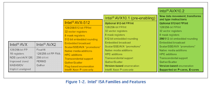


Image Source: Intel


Examining the core concept of AVX10 it signifies that consumer-based desktop chips will now have full AVX-512 support. Although performance (P) cores have the theoretical capability to support 512-bit wide vectors if Intel desires (Intel has currently confirmed support is up to 256-bit vectors), efficiency (E) cores are restricted to 256-bit vectors. Nevertheless, as a whole, the entire chip will be capable of supporting complete AVX-512 instruction sets across all of the cores, whether they are fully-fledged performance or lower-powered efficiency cores.


Touching on performance, within the AVX10 technical paper, Intel states the following:


  • Intel AVX2-compiled applications, re-compiled to Intel AVX10, should realize performance gains without the need for additional software tuning.
  • Intel AVX2 applications sensitive to vector register pressure will gain the most performance due to the 16 additional vector registers and new instructions.
  • Highly-threaded vectorizable applications are likely to achieve higher aggregate throughput when running on E-core-based Intel Xeon processors or on Intel® products with performance hybrid architecture.


Intel further claims that their chips, already utilizing 256-bit vectors as an example, will maintain similar performance levels when compiled onto AVX10 at the 256-bit ISO vector length. However, the true potential of AVX10 comes to light when leveraging the more substantial 512-bit vector length, promising the best AVX10 instruction set performance attainable. This aligns with introducing new AVX10 libraries and enhanced tool support, enabling application developers to compile newer AI and scientific-focused codes for optimal benefits. Additionally, this means preexisting libraries can be recompiled with AVX10/256 compatibility and, when possible, further optimized to exploit the larger vector units for better performance throughput.


In Intel’s first phase of AVX10 (AVX10.1), this will be introduced for early software enablement and will support the subset of Intel’s AVX-512 instruction sets, with Granite Rapids (6th Gen Xeon) performance (P) cores being the first cores to be forward compatible with AVX10. It is worth noting that AVX10.1 will not enable 256-bit embedded routing. As such, AVX10.1 will serve as an introduction to AVX10 to enable forward compatibility and implementation of the new versioning enumeration scheme.
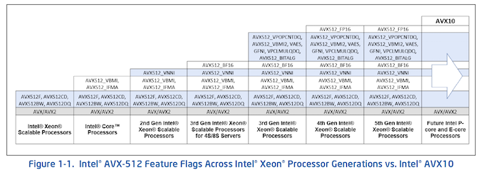


Image source: Intel


Intel’s 6th Gen Xeons, codenamed Granite Rapids, will enable AVX10.1, and future chips after this will bring fully-fledged AVX10.2 support, with AVX-512 also being supported to allow for compatibility for legacy instruction sets and applications compiled with them. It is worth noting that despite Intel AVX10/512 including all of Intel’s AVX-512 instructions, applications compiled to Intel AVX-512 with vector lengths limited to 256-bit are not guaranteed to work with an AVX10/256 processor due to differences in the supported mask register width.


While initial support of the AVX10 instruction set is more of a transitional phase in AVX10.1, it’s when AVX10.2 finally rolls out will be where AVX10 will start to show cause and effect in performance and efficiency, at least with compatible instruction sets associated with AVX10. AVX10, by default, will allow developers that recompile their preexisting code to work with AVX10, as new processors with AVX10 won’t be able to run AVX-512 binaries as they previously would have. Intel is finally looking toward the future.


The introduction of AVX10 completely replaces the AVX-512 superset. Once AVX10 is widely available through Intel’s future product releases, there’s technically no need to use AVX-512 going forward. One challenge this presents is that software developers who have specifically compiled libraries specifically for 512-bit wide vectors will need to recompile the code as previously mentioned to properly work with the 256-bit wide vectors that AVX10 holistically supports across the cores.


While AVX-512 isn’t going anywhere as an instruction set, it’s worth highlighting that AVX10 is backward compatible, which is an essential aspect of supporting instruction sets with various vector widths such as 128, 256, and 512-bit where applicable. Developers can recompile code and libraries for the broader transition and convergence to the AVX10 unified instruction set going forward.


Intel is committing to supporting a maximum vector size of at least 256-bit on all Intel processors in the future. Still, it remains to be seen which SKUs (if any) and the underlying architecture will support full 512-bit vector sizes in the future, as this is something Intel hasn’t officially confirmed at any point.


The meat and veg of Intel’s new AVX10 instruction set will come into play when AVX10.2 is phased in, officially bringing 256-bit instruction vector support across all cores, whether performance and/or efficiency cores. This also marks the inclusion of 128-bit, 256-bit, and 512-bit integer divisions across both the performance and efficiency cores, and as such, will support full vector extensions based on the specification of each core.


Source: AnandTech – Intel Unveils AVX10 and APX Instruction Sets: Unifying AVX-512 For Hybrid Architectures

Crucial X9 Pro and X10 Pro High-Performance Portable SSDs Announced

Crucial’s X6 and X8 Portable SSDs have been attractive budget options for the mainstream consumers looking to purchase high-capacity direct-attached storage drives. The company has been delivering some industry-firsts in these drives. However, these drives use QLC and are not particularly attractive for power users (such as content creators) who require writing vast amounts of data as quickly as possible.


Over the last few quarters, the company has been actively trying to introduce high-performance flash products in the client market. As an example, Crucial’s T700 Gen 5 internal SSD is the only M.2 SSD available in retail to reach the 14 GBps mark. The company is introducing two new products in the PSSD category today – the USB 3.2 Gen 2 X9 Pro, and the USB 3.2 Gen 2×2 X10 Pro. These 1 GBps and 2 GBps-class drives come with a Type-C port and a Type-C to Type-C cable (Type-A adapter sold separately). The performance specifications of these two products indicate suitability for power users – for the first time, the company is quoting write speeds for their PSSDs in the marketing material.


The X9 Pro is a 38g 65mm x 50mm USB 3.2 Gen 2 PSSD made of anodized aluminum. It includes a lanyard hole (with the LED near the hole, rather than near the Type-C port) and a rubberized soft-touch base for protection against bumps. The sides are slightly recessed for better traction during handling. It is IP55 rated, and drop-proof up to 7.5′. The PSSD supports hardware encryption (Windows BitLocker-compatible, but Crucial’s own software to set passwords will become available later this year). The company claims speeds of up to 1050 MBps reads and 1050 MBps writes, with a minimum of 970 MBps for a whole drive fill using sequential writes.


Micron’s Competitive Positioning of the X9 Pro (Vendor Claims)


The X10 Pro is a 42g 65mm x 50mm USB 3.2 Gen 2×2 PSSD, with a very similar industrial design to the X9 Pro (retaining almost all of the features). The extra weight is contributed by some internal changes for a better thermal solution. Read speeds of up to 2100 MBps and write speeds of up to 2000 MBps are claimed, though there is no minimum sequential write speed guaranteed.


Micron’s Competitive Positioning of the X10 Pro (Vendor Claims)


The X9 Pro and X10 Pro both utilize the Silicon Motion SM2320 native UFD controller. We had previewed its performance (and that of the Kingston XS2000 based on it) using Micron’s 96L 3D TLC NAND. More recently, the Transcend ESD310C was evaluated with the same controller and Kioxia’s BiCS5 112L 3D TLC NAND. Micron is able to claim much better long-term performance consistency compared to these products because of the use of their 176L 3D TLC NAND. The form-factor and size do point to the possibility of thermal throttling, which is possibly the reason for Crucial not claiming any minimum sustained write speeds for the 20 Gbps product. We will get to know further during the course of our hands-on evaluation.


Seagate was one of the first vendors to bundle a free month of Adobe Creative Cloud and Mylio Photos with select direct-attached storage drives. Micron is adopting the same value additions for the X9 Pro and X10 Pro, and also including a copy of Acronis True Image for Crucial for free.


Crucial X9 Pro and X10 Pro Pricing
X9 Pro SKU Product Link X10 Pro SKU Product Link
CT1000X9PROSSD9 (1 TB) $80 CT1000X10PROSSD9 (1 TB) $120
CT2000X9PROSSD9 (2 TB) $130 CT2000X10PROSSD9 (2 TB) $170
CT4000X9PROSSD9 (4 TB) $240 CT4000X10PROSSD9 (4 TB) $290


Pricing varies from $80 for the 1 TB version of the X9 Pro to $290 for the 4 TB version of the X10 Pro, and the drives are available for purchase today. The flash industry is currently in a bust cycle, and pricing is quite low. While that is not great news for the manufacturers, it is good news for consumers. The introduction of the X9 Pro and X10 Pro at attractive price points finally brings some competition to the SanDisk Extreme / Samsung T7 Shield in the 1 GBps category and the SanDisk Extreme PRO v2 in the 2 GBps category. While the SanDisk offerings with a bridge-based design will probably perform better for a wider variety of workloads, the Micron offerings are bound to have an advantage in terms of physical footprint and power consumption.


Source: AnandTech – Crucial X9 Pro and X10 Pro High-Performance Portable SSDs Announced

TSMC to Build $2.87 Billion Facility For Advanced Chip Packaging

TSMC on Tuesday announced plans to construct a new advanced chip packaging facility in Tongluo Science Park. The company intends to spend around $2.87 billion on the fab that will employ some 1,500 people when it becomes operational several years from now.


“To meet market needs, TSMC is planning to establish an advanced packaging fab in the Tongluo Science Park,” a statement by TSMC reads. “TSMC expects to invest nearly NT$90 billion for the project, and create 1,500 job opportunities. The Science Park Administration has officially agreed to TSMC’s application to lease land at the Tongluo Science Park, and is arranging for a lease briefing.”


The chip packing site itself is not expected to come online for several years. TSMC has yet to even begin ground preparations, and while the company isn’t announcing a formal date for project completion, local Taiwanese media has been reporting that the fab will come online some time in 2027.


Otherwise, the nearly $2.9 billion price tag implies that this will be yet another significant capital expansion project for TSMC – rivaling what would have been the cost of a wafer lithography fab a decade ago. Given TSMC’s product roadmaps as well as projections for the growing need for advanced packaging types in the coming years, the new chip packaging plant will likely be a comprehensive facility offering 3DFabric integration of front-end to back-end processes, as well as testing services.


It is likely that the new Tongluo fab will be akin TSMC’s recently opened Advanced Backend Fab 6 that is designed to support TSMC-SoIC (System on Integrated Chips) process technology, which includes such frontend 3D stacking techniques as chip-on-wafer (CoW) and wafer-on-wafer (WoW) as well as such backend packaging technologies like integrated fan-out (InFO) and chip-on-wafer-on-substrate (CoWoS).


TSMC’s InFO and CoWoS packaging technologies are currently used for chips like Apple’s M2 Ultra, AMD’s Instinct MI300, and NVIDIA’s A100 and H100 GPUs. Demand for the latter is booming these days and TSMC admitted just last week that the company barely has enough CoWoS capacity to meet it. As things stand, the company is working hard to double its CoWoS capacity by the end of 2024.


“But for the back end, the advanced packaging side, especially for the CoWoS, we do have some very tight capacity to — very hard to fulfill 100% of what customers needed,” said C.C. Wei, chief executive of TSMC, at the company’s earnings call last week. “So we are working with customers for the short term to help them to fulfill the demand, but we are increasing our capacity as quickly as possible. And we expect these tightness somewhat be released in next year, probably towards the end of next year. […] I will not give you the exact number [in terms of processed wafers capacity], but CoWoS [capacity will be doubled in 2024 vs. 2023].


TSMC’s Advanced Backend Fab 6 can process about one million 300-mm wafers per year, as well as handle over 10 million hours of testing per year. Production capacity of the upcoming packaging fab is unknown, though it is reasonable to expect TSMC to make it even bigger as importance of advanced packaging is growing.


Source: AnandTech – TSMC to Build .87 Billion Facility For Advanced Chip Packaging

Cadence Buys Memory and SerDes PHY Assets from Rambus

In a surprising turn of events, Cadence and Rambus entered into a definitive agreement late last week for Cadence to buy memory physical interface IP and SerDes businesses from Rambus. As a result, Cadence will get a comprehensive portfolio of memory PHY IP and an established client base. Meanwhile, with the sale of its PHY and SerDes assets, Rambus will now solely focus on licensing digital IP.


Historically, Rambus developed memory technologies, including RDRAM and XDR DRAM. At some point, the company patented fundamental technologies enabling SDRAM, DDR SDRAM, and their successors. Doing this allowed them to effectively sue virtually all memory makers and designers of memory controllers (including AMD and Nvidia) and make them pay license fees.


Over time the company began to license memory controllers and PHY. It became a one-stop shop for chip developers needing a turnkey memory, PCIe, or MIPI solution for their designs. Nowadays, it is possible to come to Rambus and get one of the industry’s best memory controllers and silicon-proven interfaces. But while Rambus plans to retain memory and interface controllers and everything logic-related, it intends to get rid of its PHY and SerDes IP assets and sell them to Cadence.


Getting silicon-proven PHY and SerDes IP assets and clients for Cadence makes perfect sense.


The acquisition of the Rambus PHY IP broadens Cadence’s well-established enterprise IP portfolio and expands its reach across geographies and vertical markets, such as the aerospace and defense market, providing complete subsystem solutions that meet the demands of our worldwide customers,” said Boyd Phelps, senior vice president and general manager of the IP Group at Cadence.


But the rationale behind Rambus’s decision to sell PHY and SerDes business is less obvious. On the one hand, memory PHY and SerDes businesses require Rambus to invest in expensive tape-outs on the latest nodes, and this requires capital and increases risks as Rambus has to compete against companies like Cadence and Synopsys that are larger and have more money. On the other hand, Rambus can be a one-stop shop for memory controllers and PHY, which has advantages (i.e., Rambus can charge a premium).


Meanwhile, without needing to keep its physical IP assets up to date, Rambus can now focus on licensing pure technologies and no longer invest in physical IP like PHY or SerDes.


With this transaction, we will increase our focus on market-leading digital IP and chips and expand our roadmap of novel memory solutions to support the continued evolution of the data center and AI,” said Sean Fan, senior vice president and chief operating officer at Rambus.


The transaction is projected to have a negligible impact on the revenue and earnings of each company for this year. The anticipated closing date is in the third quarter of 2023, subject to specific closing conditions.


Source: Cadence


Source: AnandTech – Cadence Buys Memory and SerDes PHY Assets from Rambus

AMD Launches Ryzen 5 7500F in China: Zen 4 With no Integrated Graphics

Over the weekend, AMD officially listed the Ryzen 5 7500F processor on their website. Although initial reports pointed towards a China-only release, and at present, that much is true, the Ryzen 5 7500F is heading towards global availability, at least according to AMD. With a reported MSRP of around $179, the Ryzen 5 7500F is currently the cheapest Zen 4-based desktop processor. It comes with six Zen 4 cores and is similar in specifications to the Ryzen 5 7600, albeit with a few variances. Most importantly, it doesn’t feature AMD’s RDNA 2 integrated graphics, as seen on other Ryzen 7000 SKUs.


When AMD initially launched their Ryzen 7000 desktop processors based on their latest Zen 4 microarchitecture in September last year, they received many performance and power efficiency plaudits. One area that didn’t shine so brightly was in value, as AMD’s Ryzen 7000 processors only support DDR5, and at the time, AMD’s new (at the time) AM5 platform was hardly cheap. Fast forward to now, and AMD looks to rectify that with their first sub $200 chip based on Zen 4, the Ryzen 5 7500F.


AMD Ryzen 5 Series Line-Up (Sub $300)
AnandTech Cores

Threads
Base

Freq
Turbo

Freq
Memory

Support
L3

Cache
TDP PPT Price $
Ryzen 5 7600X 6C / 12T 4.7 GHz 5.3 GHz DDR5-5200 32 MB 105 W 142 W $299
Ryzen 5 7600 6C / 12T 3.8 GHz 5.1 GHz DDR5-5200 32 MB 65 W 88 W $227
Ryzen 5 7500F 6C / 12T 3.7 GHz 5.0 GHz DDR5-5200 32 MB 65 W 88 W $179?*


*Price as reported by Toms Hardware & TechPowerUp


Despite only being available at the time of writing in the Chinese market, the AMD Ryzen 5 7500F benefits from six Zen 4 cores (and 12 threads), as well as a base frequency of 3.7 GHz and a turbo of up to 5.0 GHz. As with other Ryzen 5 models, such as the 7600X and 7600, the 7500F also has 32 MB of L3 cache. It also aligns with the more efficient Ryzen 5 7600 and, as such, has a 65 W base TDP with a Package Power Tracking (PPT) of up to 88 W.


The most significant difference between the Ryzen 5 7500F and the other Ryzen 7000 series processors is it seems to be the first Zen 4-based CPU to omit integrated graphics. Although the other Ryzen 7000 series chips use RDNA 2-based integrated graphics, which, although not good enough to game with at decent frame rates, does provide other benefits as it is more than powerful enough to operate typical desktop work. The Ryzen 5 7500F does retain all the other benefits of the Zen 4 and AM5 platform, such as 28 x PCIe 5.0 lanes and support for a fully-fledged high-performance PCIe 5.0 x4 M.2 SSD.


All currently associated reviews of the Ryzen 5 7500F are from Chinese and South Korean media outlets. As we mentioned, this is because, technically, the only place users can currently buy this chip is in China. Still, things point to a subsequent global launch further down the line or imminently in other regions such as North America and Europe.


Source: AnandTech – AMD Launches Ryzen 5 7500F in China: Zen 4 With no Integrated Graphics

TSMC: 3nm Chips for Smartphones and HPCs Coming This Year

While TSMC formally started mass production of chips on its N3 (3nm-class) process technology late last year, the company is set to finally ship the first revenue wafers in the current quarter. During the most recent earnings call with analysts and investors, the company said that demand for 3 nm products was steady, and that numerous designs for smartphones and high-performance applications are incoming later this year. Furthermore, N3E manufacturing node is on track for high-volume manufacturing later this year.


“We are seeing robust demand for N3 and we expect a strong ramp of N3 in the second half of this year, supported by both HPC and smartphone applications,” said C.C. Wei, chief executive officer of TSMC, during the company’s earnings. Call with financial analysts and investors.


Previously the company never commented on applications that use its initial N3 fabrication process, but for now it actually disclosed that devices that are in mass production are designed for smartphones as well as HPC applications, which is a vague term which TSMC uses to describe everything from handheld game consoles all the way to heavy-duty smartphone SoCs. 


For customer privacy reasons, TSMC does not disclose which customers are using N3. Though historically, Apple has been TSMC’s alpha client for its leading-edge process technologies, so they’re the most likely candidate to be the biggest consumer of TSMC’s N3 output. 


TSMC’s baseline N3 node (aka N3B) is an expensive technology to use. It features up to 25 EUV layers (according to China Renaissance and SemiAnalysis) with TSMC using EUV double-patterning on some of them to make for higher logic and SRAM transistor density than N5. EUV steps are expensive in general, and EUV double patterning drives those costs up further, which is why this fabrication process is only expected to be used by a handful of customers who are not as concerned about the high expenditure required. 


For those who are more cost sensitive, there is N3E, which can ‘only’ use up to 19 EUV layers and does not use EUV double patterning. Good news is that TSMC expects to commence mass production on this node to Q4 2023.


N3E has passed qualification and achieved performance and yield target and will start volume production in the fourth quarter of this year,” said Wei.


Source: TSMC


Source: AnandTech – TSMC: 3nm Chips for Smartphones and HPCs Coming This Year

Ultra Ethernet Consortium Formed, Plans to Adapt Ethernet for AI and HPC Needs

This week the Linux Foundation has announced that the group will be overseeing the formation of a new Ethernet consortium, with a focus on adapting and refining the technology for high performance computing workloads. Backed by founding members AMD, Arista, Broadcom, Cisco, Eviden, HPE, Intel, Meta and Microsoft, the new Ultra Ethernet Consortium will be working to improve Ethernet to meet the low latency and scalability requirements that HPC and AI systems need – and which the group says current Ethernet technology isn’t quite up to the task for.


The top priority of the new group will be to define and develop what they are calling the Ultra Ethernet Transport (UET) protocol, a new transport-layer protocol for Ethernet that will better address needs of AI and then HPC workloads.


Ethernet is certainly one of the most ubiquitous technologies around, but demands of AI and HPC clusters are growing so fast that the technology will run out of steam in the future. The size of large AI models is increasing rapidly. GPT-3 was trained with 175 billion of parameters back in 2020. Today GPT-4 is said to be accommodating already a trillion of parameters. Models with the larger number of parameters require larger clusters and then these clusters send larger messages over the network. As a result, the higher bandwidth and the shorter latency these network feature, the more efficient the cluster can operate.


“Many HPC and AI users are finding it difficult to obtain the full performance from their systems due to weaknesses in the system interconnect capabilities,” said Dr. Earl Joseph, CEO of Hyperion Research.


At a high level, the new Ultra Ethernet Consortium is looking to refine Ethernet in a surgical manner, improving and altering only those bits and pieces necessary to achieve their goals. At its onset, the consortium is looking at improving both the software and physical layers of Ethernet technology — but without altering its basic structure to ensure cost efficiency and interoperability.


Technical goals of the consortium include developing specifications, APIs, and source code to define protocols, interfaces, and data structures for Ultra Ethernet communications. In addition, the consortium aims to update existing link and transport protocols and create new telemetry, signaling, security, and congestion mechanisms to better address needs of large AI and HPC clusters. Meanwhile, since AI and HPC workloads have a number of differences, UET will have separate profiles for appropriate deployments.


“Generative AI workloads will require us to architect our networks for supercomputing scale and performance,” said Justin Hotard, executive vice president and general manager, HPC & AI, at Hewlett Packard Enterprise. “The importance of the Ultra Ethernet Consortium is to develop an open, scalable, and cost-effective ethernet-based communication stack that can support these high-performance workloads to run efficiently. The ubiquity and interoperability of ethernet will provide customers with choice, and the performance to handle a variety of data intensive workloads, including simulations, and the training and tuning of AI models.” 


The Ultra Ethernet Consortium is hosted by the Linux Foundation, though the real work will be undertaken by its members. Between AMD, Cisco, Intel, and other founders, these companies all either design high-performance CPUs, compute GPUs, and network infrastructure for AI and HPC workloads or build supercomputers or clusters for AI and HPC applications, thus have plenty of experience with appropriate technologies. The work of UEC is set to be conducted by four working groups that will work on Physical Layer, Link Layer, Transport Layer, and Software Layer.


And while the group is not explicitly talking about Ultra Ethernet in relation to any competing technologies, the members of the founding board – or rather, who’s not a founding member – is telling. The performance goals and HPC focus of Ultra Ethernet would have it coming into direct competition with InfiniBand, which has for over a decade been the networking technology of choice for low-latency, HPC-style networks. While developed by its own trade association, NVIDIA is said to have an outsized influence on the group vis-a-vie their Mellanox acquisition a few years ago, and they are noticeably the odd man out of the new group. The company makes significant use of both Ethernet and InfiniBand internally, using both for their scalable DGX SuperPod systems.


As for the proposed Ultra Ethernet standards, UEC members are already plotting plans how to integrate the upcoming UET technology into their products.


“We are particularly encouraged by the improved transport layer of UEC and believe our portfolio is primed to take advantage of it,” said Mark Papermaster, CTO of AMD in a blog post. “UEC allows for packet-spraying delivery across multiple paths without causing congestion or head-of-line blocking, which will enable our processors to successfully share data across clusters with minimal incast issues or the need for centralized load-balancing. Lastly, UEC accommodates built-in security for AI and HPC workloads that in turn help AMD capitalize on our robust security and encryption capabilities.”


Meanwhile, for now UEC does not say when it expects to finalize the UET specification. It’s expected that the group will seek certification from the IEEE, who maintains the various Ethernet standards, so there is an additional set of hoops to jump through there.


Finally, the UEC has noted that it is looking for additional members to round out the group, and will begin accepting new member applications from Q4 2023. Along with NVIDIA, there are several other tech giants involved in AI or HPC work that are not part of the group, so that would be their next best chance to join the consortium.


Source: The Linux Foundation, The Register


­­­­


Source: AnandTech – Ultra Ethernet Consortium Formed, Plans to Adapt Ethernet for AI and HPC Needs

Cerebras to Enable 'Condor Galaxy' Network of AI Supercomputers: 36 ExaFLOPS for AI

Cerebras Systems and G42, a tech holding group, have unveiled their Condor Galaxy project, a network of nine interlinked supercomputers for AI model training with aggregated performance of 36 FP16 ExaFLOPs. The first supercomputer, named Condor Galaxy 1 (CG-1), boasts 4 ExaFLOPs of FP16 performance and 54 million cores. CG-2 and CG-3 will be located in the U.S. and will follow in 2024. The remaining systems will be located across the globe and the total cost of the project will be over $900 million.


The CG-1 supercomputer, situated in Santa Clara, California, combines 64 Cerebras CS-2 systems into a single user-friendly AI supercomputer, capable of providing 4 ExaFLOPs of dense, systolic FP16 compute for AI training. Based around Cerebras’s 2.6 trillion transistor second-generation wafer scale engine processors, the machine is designed specifically for Large Language Models and Generative AI. It supports up to 600 billion parameter models, with configurations that can be expanded to support up to 100 trillion parameter models. Its 54 million AI-optimized compute cores and massivefabric network bandwidth of 388 Tb/s allow for nearly linear performance scaling from 1 to 64 CS-2 systems, according to Cerebras.


The CG-1 supercomputer also offers inherent support for long sequence length training (up to 50,000 tokens) and does not require any complex distributed programming languages, which is common in case of GPU clusters.


“Delivering 4 exaFLOPs of AI compute at FP16, CG-1 dramatically reduces AI training timelines while eliminating the pain of distributed compute,” said Andrew Feldman, CEO of Cerebras Systems. “Many cloud companies have announced massive GPU clusters that cost billions of dollars to build, but that are extremely difficult to use. Distributing a single model over thousands of tiny GPUs takes months of time from dozens of people with rare expertise. CG-1 eliminates this challenge. Setting up a generative AI model takes minutes, not months and can be done by a single person. CG-1 is the first of three 4 ExaFLOP AI supercomputers to be deployed across the U.S. Over the next year, together with G42, we plan to expand this deployment and stand up a staggering 36 exaFLOPs of efficient, purpose-built AI compute.”


This supercomputer is provided as a cloud service by Cerebras and G42 and since it is located in the U.S., Cerebras and G42 assert that it will not be used by hostile states.


CG-1 is the first of three 4 FP16 ExaFLOP AI supercomputers (CG-1, CG-2, and CG-3) created by Cerebras and G42 in collaboration and located in the U.S. Once connected, these three AI supercomputers will form a 12 FP16 ExaFLOP, 162 million core distributed AI supercomputer, though it remains to be seen how efficient this network will be.


In 2024, G42 and Cerebras plan to launch six additional Condor Galaxy supercomputers across the world, which will increase the total compute power to 36 FP16 ExaFLOPs delivered by 576 CS-2 systems.


The Condor Galaxy project aims to democratize AI by offering sophisticated AI compute technology in the cloud.


Sources: CerebrasEE Times.


Source: AnandTech – Cerebras to Enable ‘Condor Galaxy’ Network of AI Supercomputers: 36 ExaFLOPS for AI

Solidigm Announces D5-P5336: 64 TB-Class Data Center SSD Sets NVMe Capacity Records

Advancements in flash technology have come as a boon to data centers. Increasing layer counts coupled with better vendor confidence in triple-level (TLC) and quad-level cells (QLC) have contributed to top-line SSD capacities essentially doubling every few years. Data centers looking to optimize storage capacity on a per-rack basis are finding these top-tier SSDs to be an economically prudent investment from a TCO perspective.


Solidigm was one of the first vendors to introduce a 32 TB-class enterprise SSD a few years back. The D5-P5316 utilized Solidigm’s 144L 3D QLC NAND. The company has been extremely bullish on QLC SSDs in the data center. Compared to other flash vendors, the company has continued to use a floating gate cell architecture while others moved on to charge trap configurations. Floating gates retain programmed voltage levels for a longer duration compared to charge trap (ensuring that the read window is much longer without having to ‘refresh’ the cell). The tighter voltage level retaining capability of the NAND architecture has served Solidigm well in bringing QLC SSDs to the enterprise market.


Floating gate architecture retains programmed voltage levels for a longer duration compared to charge trap, allowing QLC implementation

Source: The Advantages of Floating Gate Technology (YouTube)


Solidigm is claiming that their 192L 3D QLC is extremely competitive against TLC NAND from its competitors that are currently in the market (read, Samsung’s 136L 6th Gen. V-NAND and Micron’s 176L 3D TLC).


Solidigm segments their QLC data center SSDs into the ‘Essential Endurance’ and ‘Value Endurance’ lines. Back in May, the company introduced the D5-P5430 as a drop-in replacement for TLC workloads. At that time, the company had hinted at a new ‘Value Endurance’ SSD based on their fourth generation QLC flash in the second half of the year. The D5-P5336 announced recently is the company’s latest and greatest in the ‘Value Endurance’ line.


Solidigm’s 2023 Data Center SSD Flagships by Market Segment


The D5-P5316 used a 64KB indirection unit (IU) (compared to the 4KB used in normal TLC data center SSDs). While endurance and speeds were acceptable for specific types of workloads that could avoid sub-64KB writes, Solidigm has decided to improve matters by opting for a 16KB IU in the D5-P5336.


Thanks to the increased layer count, Solidigm is able to offer the D5-P5336 in capacities up to 61.44 TB. This takes the crown for the highest capacity in a single NVMe drive, allowing a single 1U server with 32 E1.L versions to hit 2 PB. For a 100 PB solution, Solidigm claims up to 17% lower TCO against the best capacity play from its competition (after considering drive and server count as well as total power consumption).


Solidigm D5-P5336 NVMe SSD Specifications
Aspect Solidigm D5-P5336
Form Factor 2.5″ 15mm U.2 / 7.5mm E3.S / 9.5mm E1.L
Interface, Protocol PCIe 4.0 x4 NVMe 1.4c
Capacities U.2

7.68 TB, 15.36 TB, 30.72 TB, 61.44 TB
E3.S

7.68 TB, 15.36 TB, 30.72 TB
E1.L

15.36 TB, 30.72 TB, 61.44 TB
3D NAND Flash Solidigm 192L 3D QLC
Sequential Performance (GB/s) 128KB Reads @ QD 128 7.0
128KB Writes @ QD 128 3.3
Random Access (IOPS) 4KB Reads @ QD 256 1005K
16KB Writes @ QD 256 43K
Latency (Typical) (us) 4KB Reads @ QD 1 ??
4KB Writes @ QD 1 ??
Power Draw (Watts) 128KB Sequential Read ??
128KB Sequential Write 25.0
4KB Random Read ??
4KB Random Write ??
Idle 5.0
Endurance (DWPD) 100% 128KB Sequential Writes ??
100% 16KB Random Write 0.42 (7.68 TB) to 0.58 (61.44 TB)
Warranty 5 years


Note that Solidigm is stressing endurance and performance numbers for IU-aligned workloads. Many of the interesting aspects are not yet known as the product brief is still in progress.


Ultimately, the race for the capacity crown comes with tradeoffs. Similar to hard drives adopting shingled-magnetic recording (SMR) to eke out extra capacity at the cost of performance for many different workload types, Solidigm is adopting a 16KB IU with QLC NAND optimized for read-intensive applications. Given the massive capacity per SSD, we suspect many data centers  may find it perfectly acceptable (at least, endurance-wise) to use it in other workloads where storage density requirements matter more than write performance.


Source: AnandTech – Solidigm Announces D5-P5336: 64 TB-Class Data Center SSD Sets NVMe Capacity Records

TSMC Delays Arizona Fab Deployment to 2025, Citing Shortage of Skilled Workers

TSMC on Thursday disclosed that it will have to delay mass production at its Fab 21 in Arizona to 2025, as a lack of suitably skilled workers is slowing down the installation of cleanroom tools. The company also confirmed that it is sending in hundreds of people familiar with its fabs from Taiwan to Arizona to assist the installation.


“We are encountering certain challenges, as there is an insufficient amount of skilled workers with the specialized expertise required for equipment installation in a semiconductor-grade facility,” said Mark Liu, chairman of TSMC, during the company’s earnings call with financial analysts and investors. “While we are working on to improve the situation, including sending experienced technicians from Taiwan to train local skill workers for a short period of time, we expect the production schedule of N4 process technology to be pushed out to 2025.”


Construction of TSMC’s Fab 21 phase 1 kicked off in April 2021, and reached completion a little behind schedule by the middle of 2022. In December of 2022, TSMC started moving equipment in. Normally, equipping a fab’s cleanroom requires around a year, which is why TSMC anticipated that the chip manufacturing plant would be operational by early 2024. Apparently, installation of production tools into Fab 21 encountered several setbacks as local workers were unfamiliar with TSMC’s requirements. 


As it turns out, these setbacks were so severe that TSMC now expects to need an extra year to start mass production at the fab, moving the start date from early 2024 to 2025. Which, at what’s now 18+ months out, TSMC isn’t even bothering to provide guidance about when in 2025 it expects its Fab 21 phase 1 to start mass production – only that it will happen at some point in the year.


The impact of TSMC’s Fab 21 launch delay on its U.S. customers is yet to be determined. The megafab-class facility is not nearly as large as TSMC’s flagship gigafabs in Taiwan, so the impact in terms of wafer starts is not as significant as if one of the larger fabs was delayed. The most recent estimate for Fab 21 was that it would hit 20K wafer starts per month, around one-fifth the capacity of a gigafab. So the capacity loss, while important, is not critical to TSMC’s overall production quotas. Though with TSMC expecting to be at full capacity in 2024, there may not be much capacity left to pick up the slack.


Likely to be the bigger concern is that Fab 21 was being built (and subsidized) in large part to allow TSMC to produce sensitive, US-based chip designs within the US. While non-sensitive chips can be allocated to other fabs in Taiwan (capacity permitting), that’s not going to be a suitable alternative for chips that need to be built within the US. A one-year delay on Fab 21 is likely to throw a wrench into those plans, but it will be up to TSMC’s buyers (and their government clients) on whether to accept the delay or look at alternatives.


Finally, getting back to the subject of skilled workers, late last month TSMC confirmed to Nikkei that it was in talks with the U.S. government to provide non-immigrant visas to its Taiwanese specialists to the U.S., to help at “a critical phase, handling all of the most advanced and dedicated equipment in a sophisticated facility.” According to the Nikkei report, a 500-man team of technicians was dispatched from Taiwan, arriving with hands-on expertise in a diverse range of fields. This expertise includes the installation of wafer fab tools and their synchronized operation, and, among other things, construction of fab mechanical and electrical systems.


Sources: TSMCNikkei


Source: AnandTech – TSMC Delays Arizona Fab Deployment to 2025, Citing Shortage of Skilled Workers

ASUS Signs Agreement to Continue Development and Support of Intel's NUC Business

ASUS and Intel late on Tuesday announced that they had agreed to a term sheet involving Intel’s NUC business, ensuring the continued support of existing NUC hardware as well as the development of new designs. Under the terms of the deal, ASUS will receive a non-exclusive license to existing Intel’s NUC systems designs, the right to develop future designs, and an obligation to support existing NUCs. The world’s largest motherboard supplier and one of the top 10 PC makers will thus take over a significant portion of the NUC program. 


“As we pivot our strategy to enable ecosystem partners to continue NUC systems product innovation and growth, our priority is to ensure a smooth transition for our customers and partners,” said Sam Gao, Intel vice president and general manager of Intel Client Platform Solutions. “I am looking forward to ASUS continuing to deliver exceptional products and supporting our NUC systems customers.”


“Thank you, Intel, for your confidence in us to take the NUC systems product line forward,” said Joe Hsieh, ASUS chief operating officer. “I am confident that this collaboration will enhance and accelerate our vision for the mini PC – greatly expanding our footprint in areas such as AI and AioT. We are committed to ensuring the excellent support and service that NUC systems customers expect.”


The move comes as Intel last week announced that the company will be exiting the NUC business – one of several strategic shuffles made by Intel in the past couple of years that has seen the company exit many of its non-core businesses. With Intel doubling down on chip design and fabrication, these business units have frequently been sold to other parties, such as Intel’s SSD/NAND business (now Solidigm/SK hynix) and Intel’s pre-built server business (now MiTAC).


Under the terms of the proposed deal, ASUS will form a new business unit called ASUS NUC, which will be able to produce and sell Intel’s 10th through 13th generation NUC PCs, as well as rights to develop future NUC designs. The deal also obligates ASUS to provide support for the platform, with Intel and ASUS both reiterating the importance of continued support (and business continuity) of the platform.


Curiously, the deal is explicitly nonexclusive; so despite ASUS being set up to be Intel’s successor in the NUC space, ASUS isn’t necessarily getting the NUC market to itself – though Intel isn’t announcing any other licensees at this time, either. The limited details on the deal also do not mention ASUS taking on any employees from Intel’s existing NUC group, so it seems this will not be a wholesale business unit transfer like other units such as SSDs have been.


In any case, licensing Intel’s NUC business should greatly strengthen ASUS’s position within the compact PC market. Even with their vast engineering resources and a broad lineup of products, ASUS has only offered a limited range of NUC-sized PC products. The company currently offers its PN and PB series of mini-PCs, along with some ExpertCenter desktop models that fit in the SFF category. The PN series could be termed as clones of the mainstream NUCs, and ASUS has a wide variety of notebooks that probably render the NUC Laptop Kits irrelevant. However, ASUS currently doesn’t have equivalents of the NUC Enthusiast and NUC Extreme models or the NUC Compute Elements.


Ultimately, those NUC products will be complementary to ASUS’s current lineup of mini-PCs and SFF systems, allowing ASUS to grow its overall footprint in the compact PC space. The deal is also a win for the existing NUC ecosystem, as current users are assured of support and warranties will continue to get honored.


The PN Mini-PC Series – NUC Mainstream’s ASUS Avatar


Looking forward, there is plenty of scope for continued innovation in the NUC space under ASUS. For example, allowing USB-C PD to power the NUCs, or even PoE support for the NUCs targeting industrial applications, are low-hanging fruits. ASUS is probably among the few companies in the world that can afford to continue to innovate while running the current program at scale.


One big question is who will be producing existing and future NUCs. Intel outsourced at least some of its NUCs to third parties like ECS and Pegatron under OEM deals, which is a normal practice. By contrast, ASUS outsources a significant portion of its production to Pegatron, its daughter company. We do not know who exactly produces the 10th – 13th Gen. NUCs for Intel at the moment, but if it is not Pegatron, it remains to be seen whether ASUS will continue to order systems from the current supplier, or will try to transfer production to its usual manufacturing partner.


Source: AnandTech – ASUS Signs Agreement to Continue Development and Support of Intel’s NUC Business

Samsung Completes Initial GDDR7 Development: First Parts to Reach Up to 32Gbps/pin

Samsung has announced this evening that they have completed development on their first generation of GDDR7 memory. The next iteration of the high bandwidth memory technology, which has been under industry-wide development, is expected to hit the market in 2024, with Samsung in prime position to be one of the first memory vendors out of the gate. With their first generation of GDDR7 parts slated to hit up to 32Gbps/pin of bandwidth – 33% more than their best GDDR6 parts today – the company is looking to deliver a sizable increase in GDDR memory bandwidth on the back of the technology’s adoption of PAM-3 signaling.


Samsung’s announcement comes as we’ve been seeing an increase in disclosures and announcements around the next iteration of the widely-used memory technology. While a finished specification for the memory has yet to be released by JEDEC, Samsung rival Micron has previously announced that it plans to introduce its own GDDR7 memory in 2024 – a similar timeline as to Samsung’s current schedule. Meanwhile, EDA tool firm Cadence disclosed a significant amount of technical details earlier this year as part of announcing their GDDR7 verification tools, revealing that the memory would use PAM-3 signaling and reach data rates of up to 36Gbps/pin.


With today’s announcement, Samsung has become the first of the major memory manufacturers to publicly announce that they’ve completed development of their first generation of GDDR7. And while the company tends to make these sorts of memory announcements relatively early in the bring-up process – well before memory is ready for commercial mass product – it’s none the less an important milestone in the development of GDDR7, as it means that memory and device manufacturers can begin validation work against functional hardware. As for Samsung itself, the announcement gives the Korean conglomerate a very visible opportunity to reinforce their claim of leadership within the GDDR memory industry.


Besides offering an update on the development process for GDDR7, Samsung’s announcement also provides some high-level technical details about the company’s first generation of GDDR7 – though “high-level” is the operative word as this is not by any means a technical deep dive.


GPU Memory Math
  GDDR7 GDDR6X GDDR6
B/W Per Pin 32 Gbps (Projected) 24 Gbps (Shipping) 24 Gbps (Sampling)
Chip Density 2 GB (16 Gb) 2 GB (16 Gb) 2 GB (16 Gb)
Total B/W (256-bit bus) 1024 GB/sec 768 GB/ssec 768 GB/ssec
DRAM Voltage ? 1.35 V 1.35 V
Data Rate QDR QDR QDR
Signaling PAM-3 PAM-4 NRZ (Binary)
Packaging 266 FBGA 180 FBGA 180 FBGA


According to Samsung’s announcement, they’re expecting to reach data rates as high as 32Gbps/pin. That’s 33% higher than the 24Gbps data rate the company’s top GDDR6 products can hit today. Samsung and Cadence have both previously disclosed that they expect GDDR7 memory to eventually hit 36Gbps/pin, though as with the development of GDDR6 – a full 50% faster than GDDR6 – this is likely going to take multiple generations of products.


Interestingly, this is starting much closer to projected limits of GDDR7 than we’ve seen in past generations of the memory technology. Whereas GDDR6 launched at 14Gbps and eventually scaled up to 24Gbps, Samsung wants to start at 32Gbps. At the same time, however, GDDR7 is going to be a smaller generational leap than we saw for GDDR6 or GDDR5; rather than doubling the signaling bandwidth of the memory technology over its predecessor, GDDR7 is only a 50% increase, owing to the switch from NRZ (2 state) signaling to PAM-3 (3 state) signaling.


It’s also worth noting that, at present, the fastest GDDR6 memory we see used video cards is only running at 20Gbps.Samsung’s own 24Gbps GDDR6, though announced just over a year ago, is still only “sampling” at this time. So the multitude of other GDDR6-using products notwithstanding, the effective jump in bandwidth for video cards in 2024/2025 could be more significant, depending on just what speed grades are available at the time.


As for capacity, Samsung’s first GDDR7 chips are 16Gb, matching the existing density of today’s top GDDR6(X) chips. So memory capacities on final products will not be significantly different from today’s products, assuming identical memory bus widths. DRAM density growth as a whole has been slowing over the years due to scaling issues, and GDDR7 will not be immune to that.


Samsung is also claiming that their GDDR7 technology offers a “20%-improvement in power efficiency versus existing 24Gbps GDDR6 DRAM,” though this is a broad claim where the devil is in the details. As power efficiency for DRAM is normally measured on a per-bit basis (picojoules-per-bit/pJpb), then our interpretation is that this is the figure Samsung is referencing in that claim. But whether that measurement is being made at 24Gbps (iso-bandwidth) or 32Gbps remains unclear.


Either way, the good news is that Samsung’s GDDR7 is slated to deliver a tangible increase in energy efficiency. But at only a 20% improvement in energy efficiency for a memory technology that is delivering up to 33% more bandwidth, this means that the absolute power consumption of the memory is going up versus the previous generation. Assuming Samsung’s energy efficiency figures are for GDDR7@32Gbps versus GDDR6@24Gbps, then we’d be looking at around a 7% increase in total energy consumption. Otherwise, if it’s at iso-bandwidth, then the increase in power consumption at full bandwidth could be much higher, depending on just what Samsung’s voltage/frequency curve comes out to.


Broadly speaking, this is the same outcome as we saw with the introduction of GDDR6(X), where despite the energy efficiency gains there, overall power consumption increased from one generation to the next, as energy efficiency gains are not keeping pace with bandwidth demands. Not to say that any of this is unexpected, but it means that good cooling will be even more critical for GDDR7 memory.


But for clients with strict power/cooling needs, Samsung is also announcing that they will be making a low-voltage version of their GDDR7 memory available. The company has not disclosed the nominal voltage of their GDDR7, or of its low-voltage counterpart, but we’d expect to see Samsung using the same chips clocked lower in exchange for a lower operating voltage, similar to low-voltage GDDR6.


Also missing from Samsung’s disclosure is anything on the fab process they’re using to produce the new memory. The company’s most recent GDDR6 uses their D1z process, while a recent DDR5 memory announcement from Samsung has them using their 12nm (D1b?) there. Even if we don’t know the specific node in use, Samsung is almost certainly using a newer node for GDDR7. Which means that at least some of the 20% energy efficiency gains from GDDR7 are going to be a product of the newer node, rather than intrinsic efficiency improvements from GDDR7.


Though Samsung certainly has been working on those, as well. While again quite light in details, the company notes that their GDDR7 memory employs “IC architecture optimization” to keep power and heat generation in check.


Electronics production aside, the final major innovation with Samsung’s GDDR7 will be decidedly physical: epoxy. Clearly mindful of the already high heat loads generated by existing GDDR memory clocked at its highest speeds, Samsung’s press release notes that they’re using a new epoxy molding compound (EMC) for GDDR7, which is designed to better transfer heat. All told, Samsung is claiming a 70% reduction in thermal resistance versus their GDDR6 memory, which should help ensure that a good cooler can still pull enough heat from the memory chips, despite the overall increase in heat generation.


Wrapping things up, now that initial development on their GDDR7 memory has been completed, Samsung is moving on to verification testing with their partners. According to the company, they’ll be working with key customers on verification this year; though at this point, the company isn’t saying when they expect to kick off mass production of the new memory.


Given the timing of Samsung’s announcement (as well as Micron’s), the initial market for GDDR7 seems to be AI and networking accelerators, rather than the video cards that GDDR7 gets its name from. With both AMD and NVIDIA barely a quarter of the way through their current architectural release cycles, neither company is likely be in a position to use GDDR7 in 2024 when it’s ready. Instead, it’s going to be the other users of GDDR memory such as networking products and high-performance accelerators that are likely to be first to use the technology.


Source: AnandTech – Samsung Completes Initial GDDR7 Development: First Parts to Reach Up to 32Gbps/pin

Logitech Acquires Loupedeck to Enhance Its Software Roadmap

Being a significant maker of peripherals in general and gaming peripherals in particular, Logitech cannot omit the content creators and streamers market, which is now virtually dominated by Corsair’s Elgato. On Tuesday, Logitech said that it had acquired Loupedeck, a streaming controller specialist, enabling the company to address streamers with a dedicated product. Furthermore, the company plans to use Loupedeck’s expertise beyond its controllers.


Streaming controllers is a dynamically developing and lucrative market. These controllers retail sold for $199 – $499 per unit, and the company also makes Stream Controller for Razer, which it is set to continue building even after it becomes a part of Logitech. Meanwhile, the latter gets a potentially profitable business with many opportunities beyond the gaming market.


The Loupedeck Live S Streaming Console


Loupedeck’s streaming controllers are versatile devices that run proprietary multifaceted software that supports game streaming tools like OBS, Twitch, vMix, and Ecamm Live and applications widely used by content producers. The list includes programs like Adobe Photoshop, Adobe Premiere Pro, Adobe After Effects, Final Cut Pro, and Philips Hue Bridge. They also support tens of profiles to adjust for applications and can be used for content creation flows outside the game streaming world.


Loupedeck’s integration strengthens Logitech’s ability to offer creative tools for a diverse user base, including gamers, live-streamers, YouTubers, and other creative professionals. The two companies share a skillset for creating products integrating hardware and software, though it remains to be seen how Logitech plans to use Loupedeck’s expertise. The company says the takeover will enhance its ability to deliver personalized and context-sensitive control experiences across all its devices. This may indicate that Loupedeck’s devices will continue to deliver on their promise or may imply that Loupedeck’s expertise will be used beyond its controllers. 


“This acquisition augments Logitech’s product portfolio today and accelerates our software ambitions of enabling keyboards, mice, and more to become smarter and contextually aware, creating a better experience for audiences across Logitech,” said Ujesh Desai, general manager of Logitech G, the company’s gaming unit.


One crucial detail is that Logitech plans to engage and support Loupedeck’s expanding developer community to spur additional innovation from third parties.


Joining Logitech allows us to elevate what we are doing to the next level and exponentially broaden our audience and our impact to the creative process,” said Mikko Kesti, Loupedeck’s chief executive officer.


Source: AnandTech – Logitech Acquires Loupedeck to Enhance Its Software Roadmap

ASRock Industrial NUC BOX-1360P/D5 Review: Raptor Lake-P on the Leading Edge

ASRock Industrial has been a key player in the ultra-compact form-factor PC space over the last few years. They have managed to release 4″x4″ systems based on the latest AMD and Intel platforms well ahead of other vendors. The company’s NUC BOX-1300 series was launched along with Intel’s introduction of Raptor Lake-P in January 2023. The NUCS BOX-1360P/D4 was made available in early February with minimal improvements over the NUC BOX-1200 series. The company reserved the key Raptor Lake-P updates – DDR5 support, and USB 3.2 Gen 2×2 on the Type-C ports for the D5 series. Read on for a detailed investigation into the performance profile and feature set of the NUC BOX-1360P/D5.


Source: AnandTech – ASRock Industrial NUC BOX-1360P/D5 Review: Raptor Lake-P on the Leading Edge

Samsung Foundry's 3nm and 4nm Yields Are Improving – Report

Currently, only two foundries offer their customers 3 nm and 4 nm-class process technologies: TSMC and Samsung Foundry. But business media sometimes blames Samsung Foundry for mediocre yields on leading-edge nodes, which cannot be verified. But a recent report issued by an investment banking firm claims that yields of Samsung’s 3 nm and 4 nm-class nodes are on quite decent levels. But there is a catch.


Samsung Foundry’s 4 nm-class process technology yield is now higher than 75%. In contrast, yields of chips on SF3E (3nm-class, gate-all-around early) now exceeds 60%, according to estimates in a report from Hi Investment & Securities, a member of DGB Financial Group, reports Kmib.co.kr. The same report claims that TSMC’s yields at its N4 node approach 80%, but again, this is an estimate by a researcher.


In general, information about yields at foundries cannot be verified since contract makers of chips never talk about yields publicly since they depend on several things, such as die size, performance targets, and design peculiarities. They sometimes disclose defect density publicly compared to previous nodes, but this is hardly the case for Samsung Foundry’s SF4E, SF4, SF4P, and SF3E.


Officially, Samsung Foundry only says that its SF3E process technology is in high-volume production with stable yields (possibly to address a media report from late last year which said that SF’s yields on SF3E were unstable), and the development of refined SF3 is ongoing.


We are mass producing the 1st gen 3nm process with stable yields, and, based on this experience, we are developing the 2nd gen process to secure even greater mass production capabilities,” a statement by Samsung reads.


Meanwhile, TechInsights found one of the first chips made on Samsung’s SF3E process. This is the Whatsminer M56S++ which is apparently a cryptocurrency mining chip from MicroBT, a Chinese developer. Mining chips are tiny simplistic devices with loads of regular structures and few SRAM bit cells. Such chips are easy to make and serve perfectly as pipe cleaners for the latest process technologies, so it is not surprising that Samsung Foundry is making them rather than large ASICs on its SF3E. Meanwhile, yields of small chips are, by definition, higher than yields of large ASICs made on the same node. Therefore, if yields of the Whatsminer M56S++ are at 75% or higher, it does not mean that a large smartphone or PC SoC yields will be at the same level with the same defect density.


There is an indirect confirmation that yields of Samsung’s 5 nm and 7 nm-class fabrication processes are improving. The utilization rate of Samsung Foundry’s for 5 nm-capable lines increased to 80%, and the combined utilization rate of 5nm and 7 nm-capable fabs climbed to 90% recently, up from 60% in 2022, according to a DigiTimes story that cites ET News. Again, the information comes from an unofficial source.


Typically, fabless chip designers are not inclined to use nodes with high defect densities, so if the utilization rate of 5 nm-class (Samsung’s SF4 derived from SF5) gets higher, this may indicate that they are now more intensively used by Samsung’s customers. Alternatively, this may be a sign that Samsung Foundry has customers desperate enough to increase production despite low yields due to high demand. Yet, given the current market conditions, this may not be the case.


Sources: Kmib.co.krDigiTimesTechInsights


Source: AnandTech – Samsung Foundry’s 3nm and 4nm Yields Are Improving – Report

Lenovo Develops Mini-ITX Form-Factor GeForce RTX 4060

One of design perks of NVIDIA’s GeForce RTX 4060 is its relatively low power consumption, which has allowed graphics cards makers to produce compact add-in-boards without the massive heatsink and VRM setups required by higher-end cards. At 115 Watts, the power consumption of the card is low enough that it makes even Mini-ITX-sized cards practical, which is great news for the SFF PC community. And to that end, we’ve seen a few manufacturers introduce Mini-ITX GeForce RTX 4060 designs, with Lenovo now joining them as the latest member of the club with their own Mini-ITX 4060 card.


Specifications-wise, Lenovo’s Mini-ITX GeForce RTX 4060 is exactly what you’d expect: it a stock-configuration RTX 4060 that carries NVIDIA’s AD107 graphics processor with 3072 CUDA cores that is mated to 8 GB of GDDR6 memory using a 128-but interface. Lenovo does not disclose display outputs configuration (though expect both DisplayPort and HDMI to be present), though we see an eight-pin auxiliary PCIe power connector on the back of the board.


Meanwhile, the video card is equipped with a dual-slot, single-fan cooling system, which is typical for cards in this segment. The small heatsink and single fan is a big part in what’s enabled Lenovo to build such a small card, ensuring it will fit in a Mini-ITX system (at least so long as it can accept dual-slot cards).


Overall, with its size and scale as the world’s largest PC maker, we’ve seen Lenovo designs and manufacture scores of components over the years for their own internal use, with their Mini-ITX video card being the latest example. For the moment, Lenovo’s Mini-ITX GeForce RTX 4060 is exclusively used for the company’s IdeaCentre GeekPro 2023 system that is sold on JD.com. The PC is powered by Intel’s Core i5-13400F and is outfitted with 16GB of RAM along with a 1TB SSD.


And while Lenovo is only using the card internally for now, there’s also a chance the card could eventually make it to retail as a grey market product. The large scale of the company that makes internal component production viable also means that Lenovo parts sometimes end up on etailer shelves, especially if the company has excess stock to move.


Source: AnandTech – Lenovo Develops Mini-ITX Form-Factor GeForce RTX 4060

Corsair to Enter Personalized Peripherals Market with Drop Acquisition

Corsair on Monday said that it had agreed to buy Drop, a leading maker of personalized peripherals, such as keyboards. The market for bespoke hardware is growing these days as many gamers want to have peripherals with distinctive looks and be able to modify their parts themselves. Corsair is particularly interested in keyboard-related assets of Drop.


Personalized Keyboards that can be modified by the consumer is one of the fastest growing trends in the gaming peripheral space,” said Andy Paul, Founder and CEO of Corsair. “Drop has proven to be one of the leaders in this space and with Corsair’s global footprint, we expect to significantly grow the Drop brand worldwide. We are also excited to be able to offer specialized Corsair and Elgato products to the enthusiast community that Drop is engaged with.


Drop, formerly Massdrop, specializes in crafting a range of personalized peripherals, primarily focusing on custom-made DIY keyboards, aftermarket keycaps, and desktop accessories. The company often collaborates with other hardware makers to build customized peripherals designed with community input. For example, the company has teamed up with Sennheiser, Epos, and even Focal (a maker of ultra-premium headphones) for audio gear. An interesting detail about these collaborations is that end products were cheaper than those traditionally made by Sennheiser, Epos, or Focal.


In addition, Drop recently broadened its product line to include ‘Battlestation’ items, which represent a variety of items used by gamers, starting from stands, chargers, and cables, and extending to lightbars, carrying cases, and air dusters.


Drop’s past collaborations include The Lord of The Rings and Marvel Infinity Saga for licensed keycaps, which have seen the Drop community actively selecting new color schemes, designs, and in-demand styles.


Corsair is the ideal partner to help Drop grow and continue to fulfill its purpose of creating amazing community-driven products,” said Jef Holove, CEO of Drop. “With a worldwide sales and logistics footprint, we will be able to make Drop products more widely available, faster, while retaining the enthusiast-led product development that has seen millions of fans trust Drop for their setup and hardware.


Drop is set to maintain its independent brand identity under Corsair’s umbrella. Furthermore, the Drop team will handle all ongoing warranties, purchases, and customer service inquiries.


Source: AnandTech – Corsair to Enter Personalized Peripherals Market with Drop Acquisition

Intel Foundry Services Readies Intel 16 Process: Low Power FinFET For Everyday Chips

Intel Foundry Services (IFS) this week soft-launched their new Intel 16 process technology, a 16nm-class node that will be used for the production of low-power chips for everyday workloads. The updated legacy node, derived from Intel’s existing 22FFL process tech, is aimed at cost-conscientious customers who are producing simpler chips that don’t require the performance offered by cutting-edge process nodes. Set to compete against nodes such as TSMC’s N12e, budget nodes like Intel 16 typically see wide use in a variety of fields, ranging from aerospace and defense to IoT and radios.


First revealed by Intel a couple of years back, the ramp-up of Intel 16 comes as IFS is in the process of expanding its foundry offerings in order to offer the full range of process nodes that chip designers have come to expect from a contract fab. While not at the forefront of fab discussion as cutting edge nodes are, trailing-edge and mature process nodes are still used to produce a vast number of chips year after year, often simple chips that need few upgrades and may end up in production for a decade or longer.


TSMC, for its part, earns around 25% of its revenue by making hundreds of millions of chips using 40 nm and larger nodes. For other foundries, the revenue share share of 40nm and similar process technologies is even higher: SMIC and UMC earn over 80% of their revenue on mature nodes. Those chips have very long lifecycles – to the point that TSMC has a tough time persuading its customers to start using 28nm – underscoring their importance in the overall chip ecosystem, and the need for IFS to offer some cheaper, less advanced nodes to court these chips and their designers.


IFS’s Intel 16 node targets a wide variety of applications, including application processors, analog, consumer electronics radio frequency (such as Wi-Fi and Bluetooth), mmWave, storage, military, aerospace, and government-usage chips. This FinFET-based technology is designed to hit a sweet spot between performance and cost, offering considerable transistor density and high performance thanks to its use of FinFETs, while still costing far less than leading-edge nodes where EUV machines and multi-patterning quickly drive up costs. Intel says that its 16nm-clss technology requires fewer masks as well as relatively simple back-end design rules. In essence, we’re looking at a cost-optimized amalgamation of Intel’s 22nm and 14nm nodes, bringing 22FFL a bit more forward without employing some of the more expensive aspects of 14nm.


The bulk of this week’s announcements, in turn, are focused on chip design for the new node. Leading electronic design automation (EDA) and IP providers — Ansys, Cadence, Siemense EDA, and Synopsys — are all announcing their backing of the Intel 16 process technology with their certified software flows and IP. For example, Cadence has ported a range of its IP blocks to Intel 16, including PCIe 5.0; 25G-KR Ethernet multi-protocol PHY; multi-protocol PHY for consumer applications that support standards like PCIe 3.0 and USB 3.2; multi-standard PHY for LPDDR5/4/4X memory; and MIPI D-PHY v1.2 for cameras and displays. Additionally, Synopsys also has its AI-enabled Synopsys.ai toolkit that now supports Intel 16.


With the necessary tooling now in place, chip designers can start using design, verification, and simulation tools to develop their chips on IFS’s 16nm-class fabrication technology. At this point it remains unclear when Intel expects to start fabbing chips on the Intel 16 process, though as it’s based on mature designs, it’s likely more a matter of when the first customer chip designs will be ready.


Sources: Intel, AnsysCadenceSiemense EDA, and Synopsys.


Source: AnandTech – Intel Foundry Services Readies Intel 16 Process: Low Power FinFET For Everyday Chips

The XPG Cybercore II 1300W ATX 3.0 PSU Review: A Slightly More Modest High-End PSU

Continuing our look at the first generation of ATX 3.0 power supplies, today we’re looking a slightly more modest high-end design from XPG, the CYBERCORE II 1300W. An upgrade of the previous CYBERCORE series, the CYBERCORE II series currently consists of just two 80Plus Platinum units, rated at 1.0 kW and 1.3 kW respectively.

Within XPG’s power supply lineup, the CYBERCORE II is their sub-flagship family; but you would be hard-pressed to tell just looking at the specifications. On paper there are very few differences between the CYBERCORE II and XPG’s flagship Fusion series – the most prominent difference is the lower 80Plus certification (Platinum vs Titanium), as well as the lack of a digital interface, and a reduced number of 12VHPWR connectors (one vs two). The net result being that, even with some scaling back, the CYBERCORE II is still intended to be highly competitive within the broader high-end PSU market.

But, perhaps most importantly, the price tag of the CYBERCORE II units is less than half that of the respective Fusion units. This makes the series a very viable option for enthusiasts who are in the market for a very powerful PSU, but are not on a limitless budget.


Source: AnandTech – The XPG Cybercore II 1300W ATX 3.0 PSU Review: A Slightly More Modest High-End PSU

ASRock Announces Taichi Lite Motherboards: Same Specs, Less RGB

Last month at Computex, ASRock unveiled two new Taichi-inspired motherboards based on a ‘lite’ approach to aesthetics and design, which they called Taichi Lite. Today, ASRock has officially announced the new Taichi Lite series motherboards to the market with two new models, the ASRock Z790 Taichi Lite (Intel) and the B650E Taichi Lite (AMD). Both models feature the same controller sets as the ‘non-lite’ variations, with two primary differences; less RGB LED lighting onboard and a more straightforward overall design.


With the large swathes of RGB-clad components, peripherals, and accessories currently on the market allowing users to create a rainbow-themed discotheque in anyone’s home, there’s another side to the spectrum. Not everyone likes lots of RGB, and when it comes to bright clusters of RGB LED lighting emanating from just about everything these days. Some vendors, such as MSI, with its Unify series of motherboards, have created RGB-less designs that are sleek, stylish, and equally adept at providing the expected performance levels.


The ASRock Z790 Taichi Lite motherboard


While ASRock hasn’t taken it as far as MSI’s Unify series by completely removing all of the RGB LEDs off of the PCB, the ASRock Taichi Lite series certainly removes many zones. Interestingly, ASRock’s adopted a simpler design with less color on the heatsinks and a broader focus on blacks, silvers, and greys for an overall cleaner look. One critical fundamental change is removing a lot of the ‘armor’ that covers the bottom half of the board, which on the original Z790 Taichi also looks good. Users that don’t want any RGB LED lighting can turn them off in the firmware or through the software included by each vendor, which is the same for most motherboards, at least ones we’ve tested over the years.


As the ASRock Z790 Taichi and the newer and lighter Z790 Taichi Lite share the exact core specifications, users can be confident that both boards should perform similarly. Some of the main specifications include an advertised 24+1+2 power delivery, with 105 A smart power stages, and support for up to DDR5-7200 memory. The ASRock Z790 Taichi Lite also has an uprated audio configuration with a Realtek ALC4082 HD audio codec doing the grunt work of the audio processing, with an ESS Sabre 9218 DAC and WIMA audio caps adding an additional layer of quality to the onboard audio capabilities. There are also two Thunderbolt 4 Type-C ports and a front panel USB 3.2×2 Type-C header, which supports 60 W fast charging.


The ASRock B650E Taichi Lite motherboard


Moving onto the ASRock B650E Taichi Lite, it follows a similar path to the Z790 Taichi Lite in that it takes a lighter approach to aesthetics compared to the corresponding model, which for this board is the regular B650E Taichi. Based on the cheaper B650E for AMD’s latest Ryzen 7000 series processors, ASRock is also advertising a large 24+2+1 power delivery, with support for DDR5-6600 memory, and has the same Realtek ALC4082/ESS Sabre 9218 DAC combination as the current generation Taichi models. There’s also one USB4 spec Type-C port, with one front panel USB 3.2 G2x2 header, but this doesn’t feature 60 W charging capabilities. 


The ASRock Z790 Taichi Lite for Intel’s 13th Gen Core series processors and the B650E Taichi Lite for AMD’s Ryzen 7000 chips include a similar networking configuration. This consists of a single Killer E3100 2.5 GbE controller and an unspecified Killer-based Wi-Fi 6E CNVi, which also support BT 5.3 devices. The ASRock Z790 Taichi Lite has an additional Ethernet port powered by an Intel I219V Gigabit Ethernet controller.


Regarding pricing, ASRock highlights that the Taichi Lite series of motherboards will be cheaper than their regular Taichi counterparts, but at the time of writing, ASRock hasn’t provided MSRPs. It is expected that both the ASRock Z790 Taichi Lite and the B650E Taichi Lite should start filtering out into retail channels immediately.


Source: AnandTech – ASRock Announces Taichi Lite Motherboards: Same Specs, Less RGB